

Page 1
1
MRF839FMOTOROLA RF DEVICE DATA
The RF Line
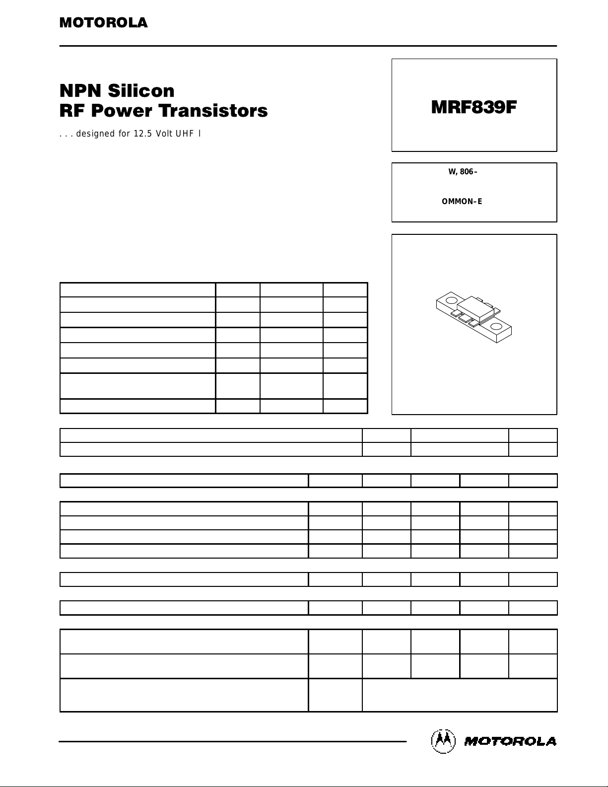
. . . designed for 12.5 Volt UHF large–signal, common–emitter amplifier
applications in industrial and commercial FM equipment operating in the range
of 806–960 MHz.
• Specified 12.5 V, 870 MHz Characteristics
Output Power = 3.0 Watts
Power Gain = 8.0 dB Min
Efficiency = 55% Min
• 100% Tested for Load Mismatch at Rated Input Power and 15.5 V
• Series Equivalent Large–Signal Characterization
• Circuit board photomaster available upon request by contacting
RF Tactical Marketing in Phoenix, AZ.
MAXIMUM RATINGS
Rating Symbol Value Unit
Collector–Emitter Voltage V
CEO
16 Vdc
Collector–Base Voltage V
CBO
36 Vdc
Emitter–Base Voltage V
EBO
3.5 Vdc
Collector Current — Continuous I
C
0.6 Adc
Operating Junction Temperature T
J
200 °C
Total Device Dissipation @ TC = 110°C
Derate above 110°C
P
D
10
111
Watts
W/°C
Storage Temperature Range T
stg
–65 to +150 °C
THERMAL CHARACTERISTICS
Characteristic Symbol Max Unit
Thermal Resistance, Junction to Case R
θJC
9.0 °C/W
ELECTRICAL CHARACTERISTICS (T
C
= 25°C unless otherwise noted.)
Characteristic
Symbol Min Typ Max Unit
OFF CHARACTERISTICS
Collector–Emitter Breakdown Voltage (IC = 5.0 mAdc, IB = 0) V
(BR)CEO
16 — — Vdc
Collector–Emitter Breakdown Voltage (IC = 5.0 mAdc, VBE = 0) V
(BR)CES
36 — — Vdc
Emitter–Base Breakdown Voltage (IE = 0.1 mAdc, IC = 0) V
(BR)EBO
3.5 — — Vdc
Collector Cutoff Current (VCE = 15 Vdc, VBE = 0, TC = 25°C) I
CES
— — 1.0 mAdc
ON CHARACTERISTICS
DC Current Gain (IC = 100 mAdc, VCE = 5.0 Vdc) h
FE
10 90 150 —
DYNAMIC CHARACTERISTICS
Output Capacitance (VCB = 15 Vdc, IE = 0, f = 1.0 MHz) C
ob
— 6.5 10 pF
FUNCTIONAL TESTS (Figure 1)
Common–Emitter Amplifier Power Gain
(P
out
= 3.0 W, VCC = 12.5 Vdc, f = 870 MHz)
G
PE
8.0 10 — dB
Collector Efficiency
(P
out
= 3.0 W, VCC = 12.5 Vdc, f = 870 MHz)
η
c
55 63 — %
Load Mismatch Stress
(VCC = 15.5 Vdc, Pin = 0.5 W, f = 870 MHz,
VSWR = 20:1, all phase angles)
ψ
No Degradation in Output Power
Order this document
by MRF839F/D
SEMICONDUCTOR TECHNICAL DATA
3.0 W, 806–960 MHz
RF POWER
TRANSISTORS
COMMON–EMITTER
NPN SILICON
CASE 319–07, STYLE 2
MRF839F
Motorola, Inc. 1994
REV 6
Page 2
MRF839F
2
MOTOROLA RF DEVICE DATA
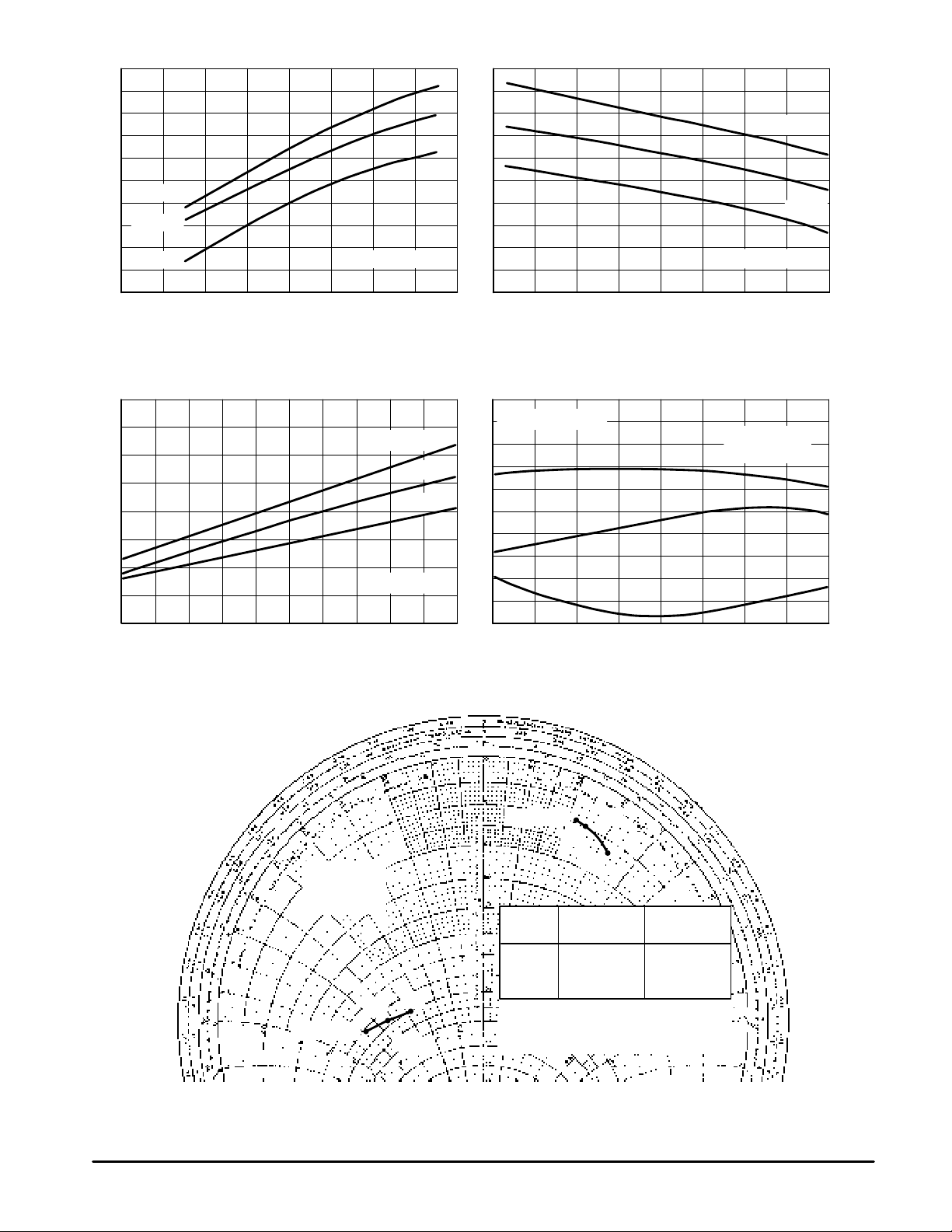
Figure 1. Output Power versus Input Power Figure 2. Output Power versus Frequency
Figure 3. Output Power versus Supply Voltage Figure 4. Broadband Performance
Figure 5. Series Equivalent Input/Output Impedances
6 8 10 12 14 16
8
6
4
2
0
800 820 840 860 880
4
3
2
1
0.5 W
fo = 870 MHz
Pin = 0.3 W
VCC = 12.5 Vdc
CIRCUIT FIGURE 14
0.25 W
1.0:1
1.5:1
2.0:1
65
60
55
VSWR
VCC, SUPPLY VOLTAGE (VOLTS)
P , OUTPUT POWER (WATTS)
out
f, FREQUENCY (MHz)
P , OUTPUT POWER (WATTS)
out
Pin = 0.75 W
η
c
(%)
f = 806 MHz
0 0.2 0.4 0.6 0.8 800 840 880 920 960
5
4
3
2
Pin, INPUT POWER (WATTS)
P , OUTPUT POWER (WATTS)
out
f, FREQUENCY (MHz)
P , OUTPUT POWER (WATTS)
out
6
1
VCC = 12.5 Vdc
870 MHz
VCC = 12.5 Vdc
VCC = 12.5 Vdc
0.5 W
Pin = 0.75 W
0.25 W
5
4
3
2
6
1
5
0
960 MHz
f = 806 MHz
ZOL*
Z
in
870
960
f = 806 MHz
870
960
Zo = 10 OHMS
P
out
= 3 WATTS
VCC = 12.5 V
ZOL* = Conjugate of the optimum load impedance
into which the device output operates at a given
output power, voltage and frequency.
f
MHz
Z
in
Ohms
ZOL*
Ohms
806
870
960
0.93 + j2.27
0.95 + j2.49
1.28 + j3.27
7.14 – j7.76
7.61 – j6.43
8.00 – j4.86
Page 3
3
MRF839FMOTOROLA RF DEVICE DATA
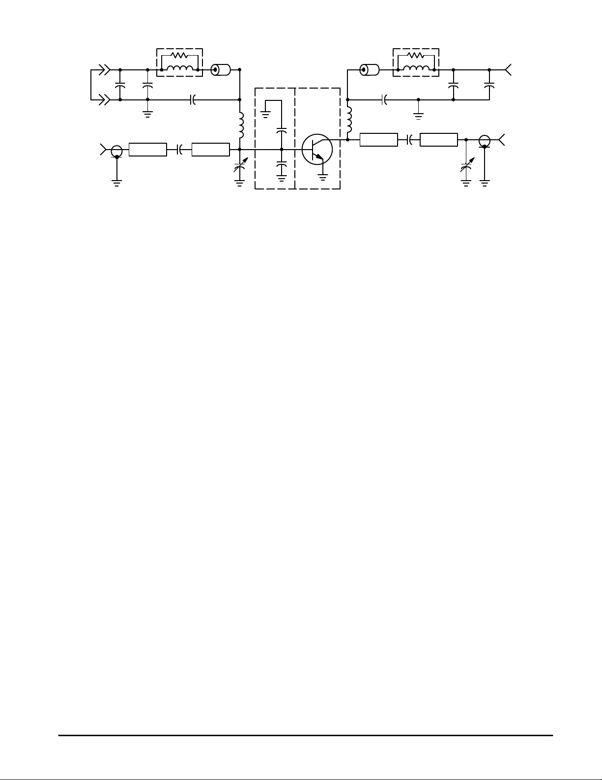
Figure 6. 800–880 MHz Broadband Test Circuit
B — Bead, Ferroxcube #56–590–65/3B
C1 — 47 pF Chip Cap (Murata Erie MA20470B)
C3, C4 — 13 pF Mini–Underwood
C5 — 51 pF Chip Cap (ATC 100B510JC500)
C2, C6 — 0.8–8.0 pF Johanson #7291
C7, C12 — 10 µF, 35 V Electrolytic Capacitor
C8, C11 — 1000 pF Unelco, J101
C9, C10 — 91 pF Mini–Underwood
L1, L2 — 4 Turns, #18 Enameled, 5/32″ ID
L3, L4 — 12 Turns, #22 Enameled over 10 Ohm, 1/2 W Carbon Resistor
Z1, Z4 — 50 Ohm Stripline
Z2 — 32 Ohm Stripline (1/4 λ @ 838 MHz)
Z3 — 16 Ohm Stripline (1/4 λ @ 838 MHz)
Board Material — 0.032″ Glass Teflon, 2 oz. Copper Clad, εr = 2.55
D.U.T.
Z1
B B
C7 C8
C5
L4
L2
C2
C3
C4
C9
C10
C1
+
+ 12.5 V
+
V
RE
PORT
50
Ω
RF INPUT
50
Ω
RF OUTPUT
C11 C12
C6
L3
Z2
Z3 Z4
SOCKET
L1
Page 4
MRF839F
4
MOTOROLA RF DEVICE DATA
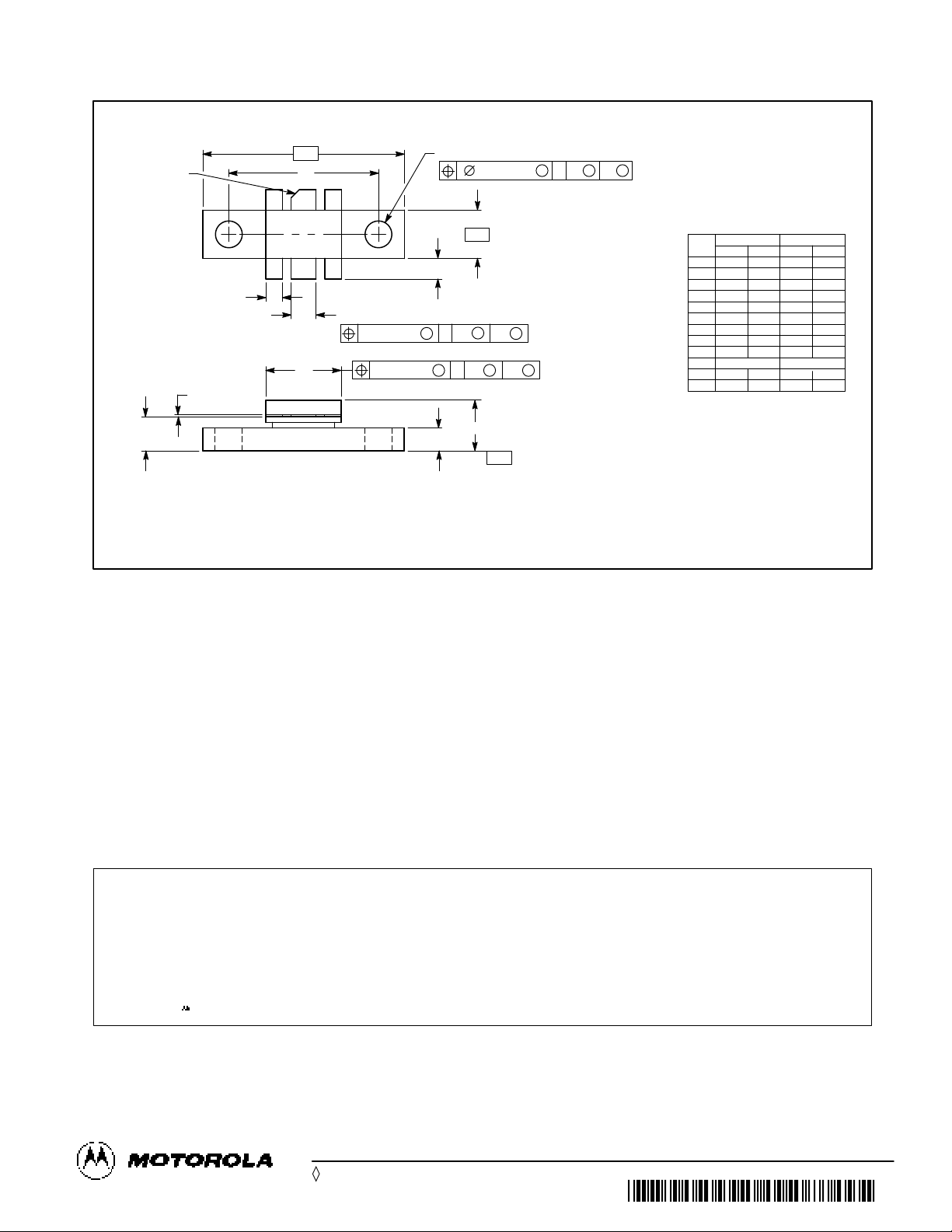
TPACKAGE DIMENSIONS
CASE 319–07
ISSUE M
0.965
0.355
0.230
0.115
0.102
0.075
0.160
0.004
0.090
0.225
0.125
0.985
0.375
0.260
0.125
0.114
0.085
0.170
0.006
0.110
0.241
0.135
24.52
9.02
5.85
2.93
2.59
1.91
4.07
0.11
2.29
5.72
3.18
25.01
9.52
6.60
3.17
2.90
2.15
4.31
0.15
2.79
6.12
3.42
MM
MIN MINMAX MAX
INCHES MILLIMETER
DIM
A
B
C
D
E
F
H
J
K
L
N
Q
NOTES:
1. DIMENSIONING AND TOLERANCING PER
ANSI Y14.5M, 1982.
2. CONTROLLING DIMENSION: INCH.
0.725 BSC 18.42 BSC
SEATING
PLANE
IDENTIFICATION
NOTCH
1 2 3
456
F
J
B
H
E
K
L
0.15 (0.006) T A N
M
-A-
-N-
-T-
Q 2 PL
D 2 PL
MM
0.38 (0.015) T A N
M
MM
0.38 (0.015) T A N
M
C
PIN 1. EMITTER (COMMON)
2. BASE (INPUT)
3. EMITTER (COMMON)
4. EMITTER (COMMON)
5. COLLECTOR (OUTPUT)
6. EMITTER (COMMON)
STYLE 2:
Motorola reserves the right to make changes without further notice to any products herein. Motorola makes no warranty, representation or guarantee regarding
the suitability of its products for any particular purpose, nor does Motorola assume any liability arising out of the application or use of any product or circuit,
and specifically disclaims any and all liability, including without limitation consequential or incidental damages. “T ypical” parameters can and do vary in different
applications. All operating parameters, including “T ypicals” must be validated for each customer application by customer’s technical experts. Motorola does
not convey any license under its patent rights nor the rights of others. Motorola products are not designed, intended, or authorized for use as components in
systems intended for surgical implant into the body, or other applications intended to support or sustain life, or for any other application in which the failure of
the Motorola product could create a situation where personal injury or death may occur. Should Buyer purchase or use Motorola products for any such
unintended or unauthorized application, Buyer shall indemnify and hold Motorola and its officers, employees, subsidiaries, affiliates, and distributors harmless
against all claims, costs, damages, and expenses, and reasonable attorney fees arising out of, directly or indirectly, any claim of personal injury or death
associated with such unintended or unauthorized use, even if such claim alleges that Motorola was negligent regarding the design or manufacture of the part.
Motorola and are registered trademarks of Motorola, Inc. Motorola, Inc. is an Equal Opportunity/Affirmative Action Employer.
Literature Distribution Centers:
USA: Motorola Literature Distribution; P.O. Box 20912; Phoenix, Arizona 85036.
EUROPE: Motorola Ltd.; European Literature Centre; 88 T anners Drive, Blakelands, Milton Keynes, MK14 5BP, England.
JAPAN: Nippon Motorola Ltd.; 4-32-1, Nishi-Gotanda, Shinagawa-ku, Tokyo 141, Japan.
ASIA PACIFIC: Motorola Semiconductors H.K. Ltd.; Silicon Harbour Center, No. 2 Dai King Street, Tai Po Industrial Estate, Tai Po, N.T., Hong Kong.
MRF839F/D
*MRF839F/D*
◊
 Loading...