

Page 1
1
MRF2000–5LMOTOROLA RF DEVICE DATA
The RF Line
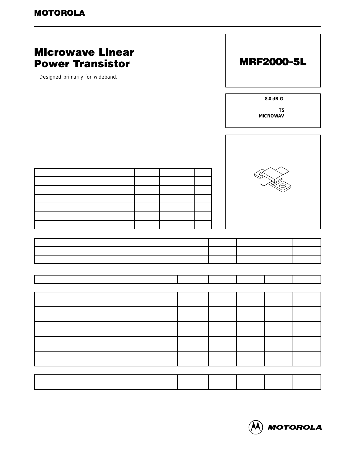
Designed primarily for wideband, large signal output and driver amplifier
stages in the 1.0 to 2.0 GHz frequency range.
• Designed for Class A or AB, Common Emitter Power Amplifiers
• Specified 20 Volt, 2.0 GHz Characteristic Power Gain —
7.0 dB Min @ 5.0 W P
out
• Built In Matching Network for Broadband Operation
• Gold Metallization for Improved Reliability
• Diffused Ballast Resistors
• Circuit board photomaster available upon request by contacting
RF Tactical Marketing in Phoenix, AZ.
MAXIMUM RATINGS
Rating Symbol Value Unit
Collector–Emitter Voltage V
CEO
22 Vdc
Collector–Base Voltage V
CES
50 Vdc
Emitter–Base Voltage V
EBO
3.5 Vdc
Collector Current — Continuous I
C
2.0 Adc
Operating Junction Temperature T
J
200 °C
Storage Temperature Range T
stg
– 65 to +150 °C
THERMAL CHARACTERISTICS
Characteristic Symbol Max Unit
Thermal Resistance, Junction to Case, DC R
θJC
(DC) 12 °C/W
Thermal Resistance, Junction to Case, RF R
θJC
(RF) 10 °C/W
ELECTRICAL CHARACTERISTICS
Characteristic Symbol Min Typ Max Unit
OFF CHARACTERISTICS
Collector–Emitter Breakdown Voltage
(IC = 50 mA, IC = 0)
V
(BR)CEO
22 — — Vdc
Collector–Emitter Breakdown Voltage
(IC = 50 mA, VBE = 0)
V
(BR)CES
50 — — Vdc
Emitter–Base Breakdown Voltage
(IE = 1.25 mA, IC = 0)
V
(BR)EBO
3.5 — — Vdc
Collector–Emitter Breakdown Voltage
(IC = 50 mA, RBE = 10 Ohms)
V
(BR)CER
35 — — Vdc
Collector Cutoff Current
(VCE = 20 V, IE = 0)
I
CBO
— — 1.25 mAdc
ON CHARACTERISTICS
DC Current Gain
(IC = 0.5 A, VCE = 5.0 V)
h
FE
20 35 100 —
(continued)
Order this document
by MRF2000–5L/D
SEMICONDUCTOR TECHNICAL DATA
7.0–8.0 dB GAIN
USABLE 1.0–2.0 GHz
5.0 WATTS
MICROWAVE
LINEAR POWER TRANSISTOR
CASE 360A–01, STYLE 2
Motorola, Inc. 1994
REV 2
Page 2
MRF2000–5L
2
MOTOROLA RF DEVICE DATA
ELECTRICAL CHARACTERISTICS — continued
Characteristic Symbol Min Typ Max Unit
FUNCTIONAL TESTS
Common–Emitter Amplifier Power Gain
(VCE = 20 V, P
out
= 5.0 W, f = 2.0 GHz, IC = 600 mA)
G
PE1
7.0 — — dB
Collector Efficiency
(VCE = 20 V, P
out
= 5.0 W, f = 2.0 GHz, IC = 600 mA)
η
c
39 — — %
Typical Class AB Performance
Common–Emitter Amplifier Power Gain
(VCE = 20 V, P
out
= 6.0 W, f = 2.0 GHz, ICQ = 100 mA)
G
PE2
— 5.0 — dB
Collector Efficiency
(VCE = 20 V, Po = 6.0 W, f = 2.0 GHz, ICQ = 100 mA)
η
c
— 48 — %
Common–Emitter Amplifier Power Gain
(VCE = 24 V, P
out
= 8.0 W, f = 2.0 GHz, ICQ = 100 mA)
G
PE3
— 6.5 — dB
Collector Efficiency
(VCE = 24 V, Po = 8.0 W, f = 2 .0 GHz, ICQ = 100 mA)
η
c
— 50 — %
VBE
APPROX. 0.85 V
VCC = 20 V
@ 600 mA
C1
L1
C2 C3 C4 C5 C6 C7 C8 C9
Z1 Z2
Z3 Z4
C10
C11
L2
RF
OUTPUT
RF
INPUT
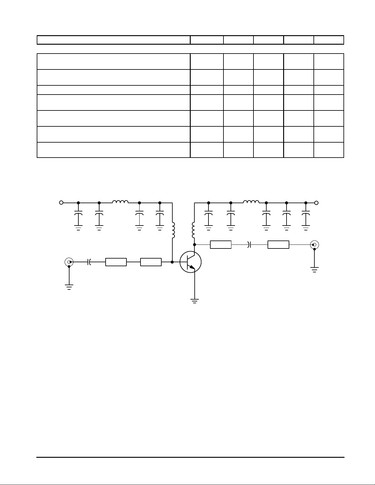
C1, C3, C5, C7 — 100pF ATC Chip Capacitor
C2, C4, C6, C8 — 0.1 µF Chip Capacitor
C9 — 50 µF Electrolytic Capacitor
C10, C11 — 28 pF ATC Chip Capacitor
L1, L2, L3 — 3 Turns, 0.125″ Dia., 18 AWG
L4 — Loop, 18 AWG
Z1, Z4 — 50r Line
Z2 — 0.55″ wide x 0.4″ Long Microstrip
Z3 — 0.4″ wide x 1.125″ Long Microstrip
PC Board — 0.018″ Teflon Fiberglass, Cu Clad ∈r = 2.55
Figure 1. 2.0 GHz Test Circuit
D.U.T.
L3 L4
Page 3
3
MRF2000–5LMOTOROLA RF DEVICE DATA
VCC = 15 V, IC = 600 mA, CLASS A
6
5
4
3
2
1
0
0 0.2 0.4 0.6 0.8 1
Pin, INPUT POWER (WATTS)
P
out
, OUTPUT POWER (WATTS)
TYPICAL CHARACTERISTICS
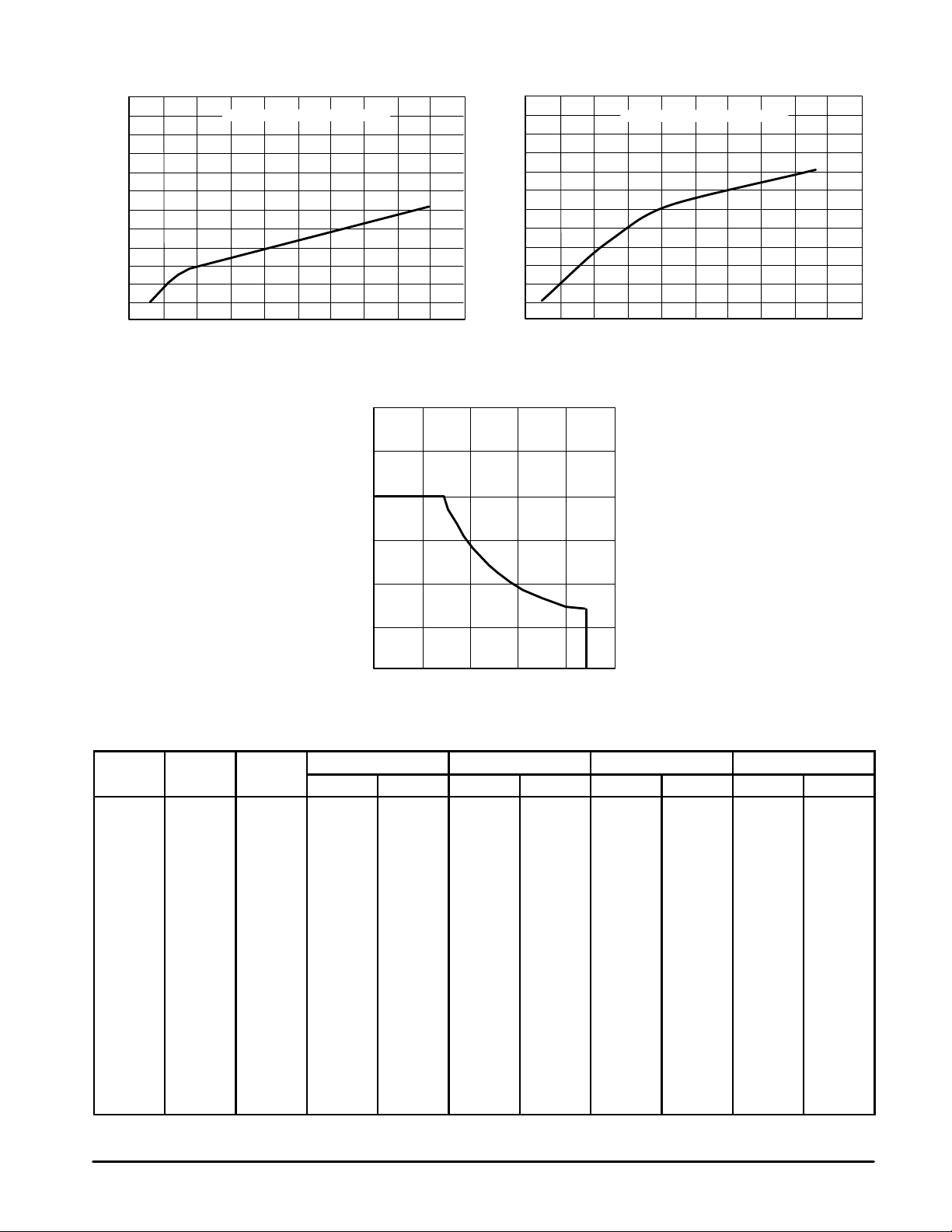
Figure 2. Output Power versus Input Power
VCC = 20 V, IC = 600 mA, CLASS A
6
5
4
3
2
1
0
0.2 0.4 0.6 0.8 1
Pin, INPUT POWER (WATTS)
P
out
, OUTPUT POWER (WATTS)
0
Figure 3. Output Power versus Input Power
2
VCE, COLLECTOR–EMITTER VOLTAGE (VOLTS)
I
C
, COLLECTOR CURRENT (AMPS)
1.5
1
0.5
0
5 10 15 20 25
Figure 4. DC Safe Operating Area
VIf
S
11
S
21
S
12
S
22
V
CE
(Vdc)
I
C
(mA)
f
MHz
|S11| ∠ φ |S21| ∠ φ |S12| ∠ φ |S22| ∠ φ
20 500 500
600
700
800
900
1000
1100
1200
1300
1400
1500
1600
1700
1800
1900
2000
2100
2200
2300
2400
2500
0.94
0.94
0.94
0.93
0.92
0.92
0.91
0.90
0.89
0.88
0.88
0.87
0.87
0.81
0.89
0.90
0.92
0.93
0.94
0.95
0.95
174
172
171
170
169
169
169
169
169
169
170
171
172
172
173
173
173
172
170
167
165
1.95
1.65
1.44
1.28
1.16
1.06
0.99
0.93
0.88
0.84
0.81
0.77
0.73
0.69
0.64
0.58
0.52
0.48
0.42
0.37
0.32
– 178
– 408
– 628
– 848
– 107
– 129
– 152
– 175
161
137
113
888
628
348
888
– 188
– 468
– 738
– 998
– 126
– 153
0.02
0.02
0.02
0.02
0.02
0.02
0.02
0.02
0.02
0.02
0.02
0.01
0.01
0.01
0.01
0.01
0.01
0.02
0.02
0.02
0.03
– 638
– 788
– 938
– 107
– 121
– 138
– 155
– 172
171
154
141
130
120
123
125
127
122
110
958
828
678
0.57
0.59
0.61
0.63
0.65
0.67
0.70
0.73
0.75
0.76
0.80
0.81
0.83
0.83
0.83
0.83
0.82
0.81
0.80
0.80
0.81
– 170
– 170
– 170
– 170
– 169
– 169
– 169
– 169
– 169
– 170
– 170
– 171
– 173
– 174
– 176
– 177
– 178
– 179
– 179
– 180
– 180
Table 1. Common Emitter S–Parameters
Page 4
MRF2000–5L
4
MOTOROLA RF DEVICE DATA
100 pF
4 plcsw
3 turns
3 plcs
20 AWG
28 pF 2 plcs
1 LOOP
18 AWG
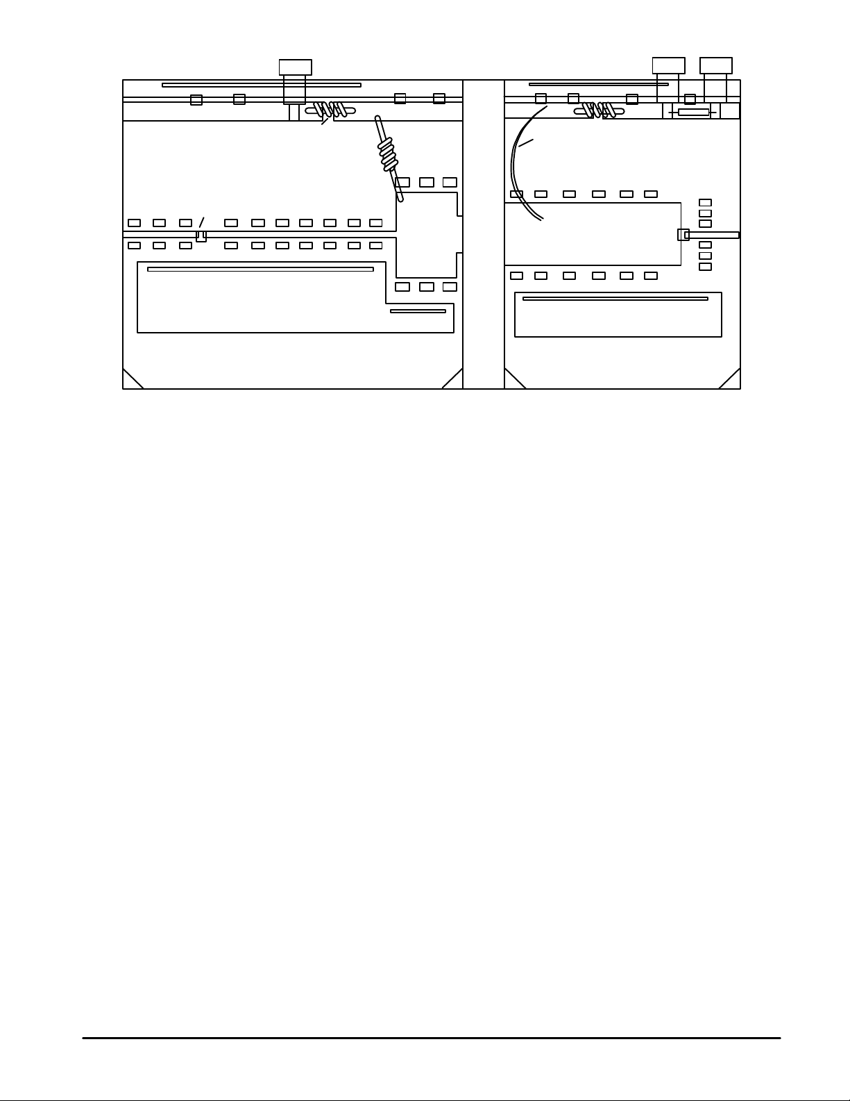
NOTE: MATERIAL IS TEFLON FIBERGLASS, 20 MIL THICK, Cu CLAD 2 SIDES
Figure 5. Test Circuit Board — Component Placement
50 µF elec.
.1
µ
F
Page 5
5
MRF2000–5LMOTOROLA RF DEVICE DATA
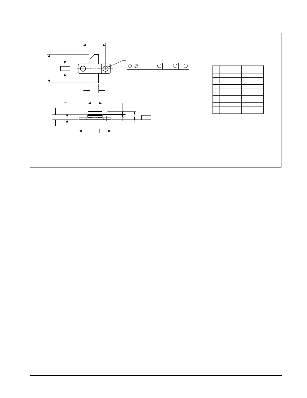
PACKAGE DIMENSIONS
CASE 360A–01
ISSUE A
NOTES:
1. DIMENSIONING AND TOLERANCING PER ANSI
Y14.5M, 1982.
2. CONTROLLING DIMENSION: INCH.
DIMAMIN MAX MIN MAX
MILLIMETERS
0.795 0.805 20.19 20.45
INCHES
B 0.225 0.235 5.71 5.97
C 0.184 0.216 4.67 5.49
D 0.210 0.220 5.33 5.59
E 0.055 0.065 1.40 1.65
H 0.115 0.135 2.92 3.43
J 0.004 0.10
K 0.670 0.730 17.02 18.54
N 0.345 0.355 8.76 9.02
Q 0.125 0.135 3.18 3.43
U 0.560 BSC 14.22 BSC
U
K
D
E
H
N
J
C
SEATING
PLANE
1
2
3
Q 2 PL
M
A
M
0.25 (0.010) B
M
T
–B–
–A–
–T–
0.006 0.15
STYLE 2:
PIN 1. COLLECTOR
2. BASE
3. EMITTER
Page 6

MRF2000–5L
6
MOTOROLA RF DEVICE DATA
How to reach us:
USA /EUROPE: Motorola Literature Distribution; JAPAN: Nippon Motorola Ltd.; Tatsumi–SPD–JLDC, Toshikatsu Otsuki,
P.O. Box 20912; Phoenix, Arizona 85036. 1–800–441–2447 6F Seibu–Butsuryu–Center, 3–14–2 Tatsumi Koto–Ku, Tokyo 135, Japan. 03–3521–8315
MFAX: [email protected] – TOUCHTONE (602) 244–6609 HONG KONG: Motorola Semiconductors H.K. Ltd.; 8B Tai Ping Industrial Park,
INTERNET: http://Design–NET.com 51 Ting Kok Road, Tai Po, N.T., Hong Kong. 852–26629298
Motorola reserves the right to make changes without further notice to any products herein. Motorola makes no warranty , representation or guarantee regarding
the suitability of its products for any particular purpose, nor does Motorola assume any liability arising out of the application or use of any product or circuit,
and specifically disclaims any and all liability, including without limitation consequential or incidental damages. “T ypical” parameters can and do vary in different
applications. All operating parameters, including “T ypicals” must be validated for each customer application by customer’s technical experts. Motorola does
not convey any license under its patent rights nor the rights of others. Motorola products are not designed, intended, or authorized for use as components in
systems intended for surgical implant into the body, or other applications intended to support or sustain life, or for any other application in which the failure of
the Motorola product could create a situation where personal injury or death may occur. Should Buyer purchase or use Motorola products for any such
unintended or unauthorized application, Buyer shall indemnify and hold Motorola and its officers, employees, subsidiaries, affiliates, and distributors harmless
against all claims, costs, damages, and expenses, and reasonable attorney fees arising out of, directly or indirectly, any claim of personal injury or death
associated with such unintended or unauthorized use, even if such claim alleges that Motorola was negligent regarding the design or manufacture of the part.
Motorola and are registered trademarks of Motorola, Inc. Motorola, Inc. is an Equal Opportunity/Affirmative Action Employer.
MRF2000–5L/D
*MRF2000-5L/D*
◊
 Loading...