

Motorola MRF141G Datasheet

SEMICONDUCTOR TECHNICAL DATA
The RF MOSFET Line
N–Channel Enhancement–Mode MOSFET
Designed for broadband commercial and military applications at frequencies
to 175 MHz. The high power, high gain and broadband performance of this
device makes possible solid state transmitters for FM broadcast or TV channel
frequency bands.
• Guaranteed Performance at 175 MHz, 28 V:
Output Power — 300 W
Gain — 12 dB (14 dB Typ)
Efficiency — 50%
• Low Thermal Resistance — 0.35°C/W
• Ruggedness Tested at Rated Output Power
• Nitride Passivated Die for Enhanced Reliability
D
Order this document
by MRF141G/D
300 W, 28 V, 175 MHz
N–CHANNEL
BROADBAND
RF POWER MOSFET
G
G
D
S
(FLANGE)
CASE 375–04, STYLE 2
MAXIMUM RATINGS
Rating Symbol Value Unit
Drain–Source Voltage V
Drain–Gate Voltage V
Gate–Source Voltage V
Drain Current — Continuous I
Total Device Dissipation @ TC = 25°C
Derate above 25°C
Storage Temperature Range T
Operating Junction Temperature T
DSS
DGO
GS
D
P
D
stg
J
65 Vdc
65 Vdc
±40 Vdc
32 Adc
500
2.85
–65 to +150 °C
200 °C
THERMAL CHARACTERISTICS
Characteristic Symbol Max Unit
Thermal Resistance, Junction to Case R
NOTE — CAUTION — MOS devices are susceptible to damage from electrostatic charge. Reasonable precautions in handling and
packaging MOS devices should be observed.
θJC
0.35 °C/W
Watts
W/°C
REV 2
Motorola, Inc. 1997
MRF141GMOTOROLA RF DEVICE DATA
1
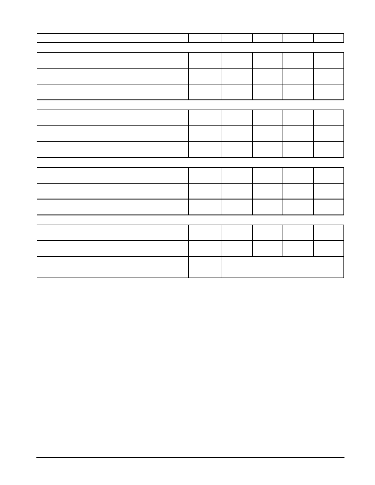
ELECTRICAL CHARACTERISTICS (T
Characteristic Symbol Min Typ Max Unit
OFF CHARACTERISTICS (1)
Drain–Source Breakdown Voltage
(VGS = 0, ID = 100 mA)
Zero Gate Voltage Drain Current
(VDS = 28 V, VGS = 0)
Gate–Body Leakage Current
(VGS = 20 V, VDS = 0)
ON CHARACTERISTICS (1)
Gate Threshold Voltage
(VDS = 10 V, ID = 100 mA)
Drain–Source On–Voltage
(VGS = 10 V, ID = 10 A)
Forward Transconductance
(VDS = 10 V, ID = 5.0 A)
DYNAMIC CHARACTERISTICS (1)
Input Capacitance
(VDS = 28 V, VGS = 0, f = 1.0 MHz)
Output Capacitance
(VDS = 28 V, VGS = 0, f = 1.0 MHz)
Reverse Transfer Capacitance
(VDS = 28 V, VGS = 0, f = 1.0 MHz)
= 25°C unless otherwise noted)
C
V
(BR)DSS
I
DSS
I
GSS
V
GS(th)
V
DS(on)
g
fs
C
iss
C
oss
C
rss
65 — — Vdc
— — 5.0 mAdc
— — 1.0 µAdc
1.0 3.0 5.0 Vdc
0.1 0.9 1.5 Vdc
5.0 7.0 — mhos
— 350 — pF
— 420 — pF
— 35 — pF
FUNCTIONAL TESTS (2)
Common Source Amplifier Power Gain
(VDD = 28 V, P
Drain Efficiency
(VDD = 28 V, P
Load Mismatch
(VDD = 28 V, P
VSWR 5:1 at all Phase Angles)
NOTES:
1. Each side measured separately.
2. Measured in push–pull configuration.
= 300 W, IDQ = 500 mA, f = 175 MHz)
out
= 300 W, f = 175 MHz, ID (Max) = 21.4 A)
out
= 300 W, IDQ = 500 mA, f = 175 MHz,
out
G
ps
η 45 55 — %
ψ
12 14 — dB
No Degradation in Output Power
MRF141G
2
MOTOROLA RF DEVICE DATA
 Loading...