

Motorola MRF1090MA, MRF1090MB Datasheet
SEMICONDUCTOR TECHNICAL DATA
The RF Line
Order this document
by MRF1090MA/D
Designed for Class B and C common base amplifier applications in short
pulse T ACAN, IFF, and DME transmitters.
• Guaranteed Performance @ 1090 MHz, 50 Vdc
Output Power = 90 Watts Peak
Minimum Gain = 8.4 dB
• 100% Tested for Load Mismatch at All Phase Angles with 10:1 VSWR
• Industry Standard Package
• Nitride Passivated
• Gold Metallized for Long Life and Resistance to Metal Migration
• Internal Input Matching for Broadband Operation
• Circuit board photomaster available upon request by contacting
RF Tactical Marketing in Phoenix, AZ.
MAXIMUM RATINGS
Rating Symbol Value Unit
Collector–Base Voltage V
Emitter–Base Voltage V
Collector–Current — Peak (1) I
Total Device Dissipation @ TC = 25°C (1) (2)
Derate above 25°C
Storage Temperature Range T
CBO
EBO
C
P
D
stg
THERMAL CHARACTERISTICS
Characteristic Symbol Max Unit
Thermal Resistance, Junction to Case (3) R
70 Vdc
4.0 Vdc
6.0 Adc
290
1.66
–65 to +150 °C
Watts
W/°C
θJC
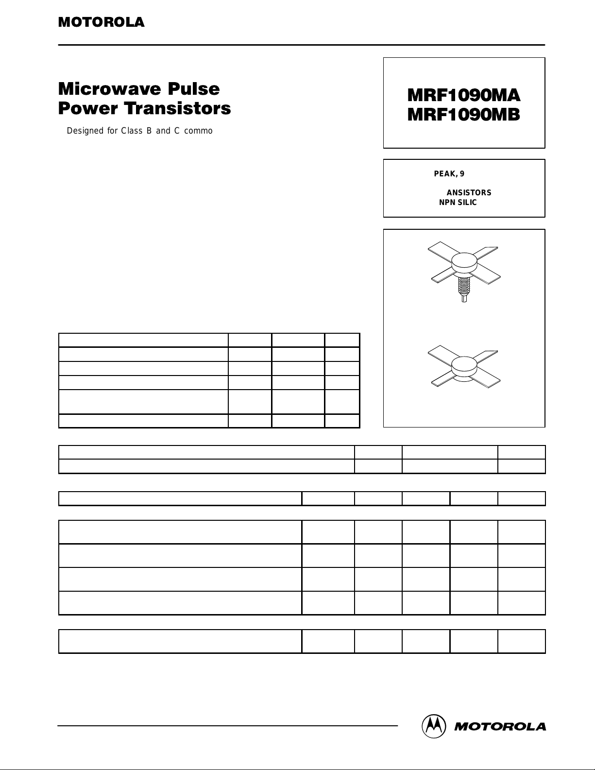
90 W PEAK, 960–1215 MHz
MICROWAVE POWER
TRANSISTORS
NPN SILICON
CASE 332–04, STYLE 1
(MRF1090MA)
CASE 332A–03, STYLE 1
(MRF1090MB)
0.6 °C/W
ELECTRICAL CHARACTERISTICS (T
Characteristic
= 25°C unless otherwise noted)
C
Symbol Min Typ Max Unit
OFF CHARACTERISTICS
Collector–Emitter Breakdown V oltage
(IC = 25 mAdc, VBE = 0)
Collector–Base Breakdown Voltage
(IC = 25 mAdc, IE = 0)
Emitter–Base Breakdown Voltage
(IE = 5.0 mAdc, IC = 0)
Collector Cutoff Current
(VCB = 50 Vdc, IE = 0)
V
(BR)CES
V
(BR)CBO
V
(BR)EBO
I
CBO
70 — — Vdc
70 — — Vdc
4.0 — — Vdc
— — 5.0 mAdc
ON CHARACTERISTICS
DC Current Gain (4)
(IC = 2.5 Adc, VCE = 5.0 Vdc)
NOTES: (continued)
1. Pulse Width = 10 µs, Duty Cycle = 1%.
2. These devices are designed for RF operation. The total device dissipation rating applies only when the device is operated as RF amplifiers.
3. Thermal Resistance is determined under specified RF operating conditions by infrared measurement techniques.
4. 80 µs Pulse on Tektronix 576 or equivalent.
REV 8
Motorola, Inc. 1997
h
FE
10 30 — —
MRF1090MA MRF1090MBMOTOROLA RF DEVICE DATA
1
ELECTRICAL CHARACTERISTICS — continued (T
Characteristic Symbol Min Typ Max Unit
= 25°C unless otherwise noted)
C
DYNAMIC CHARACTERISTICS
Output Capacitance
(VCB = 50 Vdc, IE = 0, f = 1.0 MHz)
FUNCTIONAL TESTS (Pulse Width = 10 µs, Duty Cycle = 1.0%)
Common–Base Amplifier Power Gain
(VCC = 50 Vdc, P
Collector Efficiency
(VCC = 50 Vdc, P
Load Mismatch
(VCC = 50 Vdc, P
VSWR = 10:1 All Phase Angles)
= 90 W pk, f = 1090 MHz)
out
= 90 W pk, f = 1090 MHz)
out
= 90 W pk, f = 1090 MHz,
out
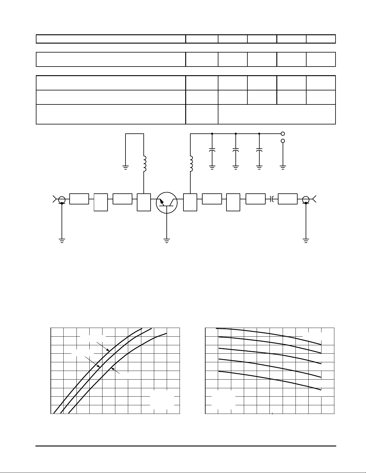
L1 L2
C
ob
G
PB
η 35 40 — %
ψ
C2 C3 C4
— 12 16 pF
8.4 10.8 — dB
No Degradation in Power Output
+
50 Vdc
+
–
RF
INPUT
120
100
80
60
40
out
P , OUTPUT POWER (W ATTS pk)
20
RF
OUTPUT
Z1
Z2
DUT
Z3
Z4 Z5
C1, C2 — 220 pF Chip Capacitor, 100–mil ATC
C3 — 0.1 µF
C4 — 47 µF/75 V
L1, L2 — 3 Turns #18 AWG, 1/8″ ID
Z1–Z9 — Distributed Microstrip Elements,
See Photomaster
Board Material — 0.031″ Thick Glass Teflon, εr = 2.5
Z6
Z7
C1
Z8 Z9
Figure 1. 1090 MHz T est Circuit
120
f = 960 MHz
1090 MHz
36912150
P
in
1215 MHz
, INPUT POWER (WATTS pk)
VCC = 50 V
tp = 10
µ
s
D = 1%
100
80
60
40
out
P , OUTPUT POWER (W ATTS pk)
20
VCC = 50 V
tp = 10
µ
s
D = 1%
960 1090 1215
f, FREQUENCY (MHz)
Pin = 10.5 W pk
9 W pk
7.5 W pk
6 W pk
4.5 W pk
Figure 2. Output Power versus Input Power Figure 3. Output Power versus Frequency
MRF1090MA MRF1090MB
2
MOTOROLA RF DEVICE DATA
 Loading...