

Motorola MRF10500, MRF10501 Datasheet
2–1
MRF10500 MRF10501MOTOROLA RF DEVICE DATA
The RF Line
. . . designed for 1025 –1150 MHz pulse common base amplifier applications
such as TCAS, TACAN and Mode–S transmitters.
• Guaranteed Performance @ 1090 MHz
Output Power = 500 Watts Peak
Gain = 8.5 dB Min, 9.0 dB (Typ)
• 100% Tested for Load Mismatch at All Phase Angles with 10:1 VSWR
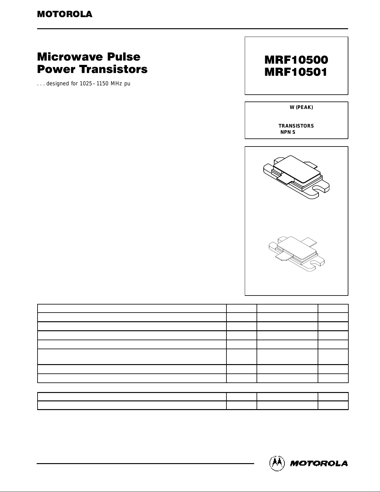
• Hermetically Sealed Industry Package
• Silicon Nitride Passivated
• Gold Metallized, Emitter Ballasted for Long Life and Resistance to Metal
Migration
• Internal Input and Output Matching
• Characterized with 10 µs, 1% Duty Cycle Pulses
MAXIMUM RATINGS
Rating Symbol Value Unit
Collector–Emitter Voltage V
CES
65 Vdc
Collector–Base Voltage V
CBO
65 Vdc
Emitter–Base Voltage V
EBO
3.5 Vdc
Collector Current — Peak (1) I
C
29 Adc
Total Device Dissipation @ TC = 25°C (1), (2)
Derate above 25°C
P
D
1460
8.3
Watts
W/°C
Storage Temperature Range T
stg
–65 to +200 °C
Junction Temperature T
J
200 °C
THERMAL CHARACTERISTICS
Characteristic Symbol Max Unit
Thermal Resistance, Junction to Case (3) R
θJC
0.12 °C/W
NOTES:
1. Under pulse RF operating conditions.
2. These devices are designed for RF operation. The total device dissipation rating applies only when the devices are operated as pulsed RF
amplifiers.
3. Thermal Resistance is determined under specified RF operating conditions by infrared measurement techniques. (Worst case θJC value
measured @ 32 µs, 2%.)
Order this document
by MRF10500/D
SEMICONDUCTOR TECHNICAL DATA
500 W (PEAK)
1025–1150 MHz
MICROWAVE POWER
TRANSISTORS
NPN SILICON
CASE 355D–02, STYLE 1
MRF10500
CASE 355H–01, STYLE 1
MRF10501
Motorola, Inc. 1994
REV 6
MRF10500 MRF10501
2–2
MOTOROLA RF DEVICE DATA
ELECTRICAL CHARACTERISTICS (T
C
= 25°C unless otherwise noted.)
Characteristic
Symbol Min Typ Max Unit
OFF CHARACTERISTICS
Collector–Emitter Breakdown Voltage (IC = 60 mAdc, VBE = 0) V
(BR)CES
65 — — Vdc
Collector–Base Breakdown Voltage (IC = 60 mAdc, IE = 0) V
(BR)CBO
65 — — Vdc
Emitter–Base Breakdown Voltage (IE = 10 mAdc, IC = 0) V
(BR)EBO
3.5 — — Vdc
Collector Cutoff Current (VCB = 36 Vdc, IE = 0) I
CBO
— — 25 mAdc
ON CHARACTERISTICS
DC Current Gain (IC = 5.0 Adc, VCE = 5.0 Vdc) h
FE
20 — — —
FUNCTIONAL TESTS
Common–Base Amplifier Power Gain
(VCC = 50 Vdc, P
out
= 500 W Peak, f = 1090 MHz)
G
PB
8.5 9.0 — dB
Collector Efficiency
(VCC = 50 Vdc, P
out
= 500 W Peak, f = 1090 MHz)
η 40 45 — %
Load Mismatch
(VCC = 50 Vdc, P
out
= 500 W Peak, f = 1090 MHz,
VSWR = 10:1 All Phase Angles)
ψ No Degradation in Output Power
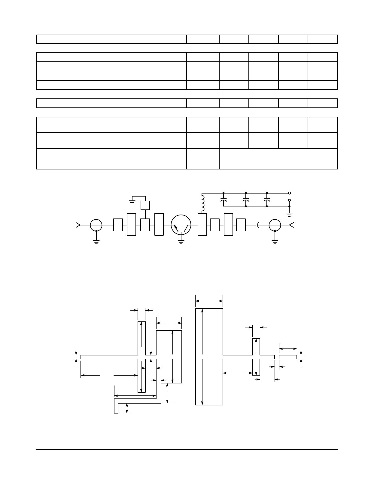
Figure 1. Test Circuit
RF INPUT
RF OUTPUT
Z1 Z2 Z3 Z4
Z5
Z6 Z7 Z8 Z9
C2 C3 C4
+
+
–
C1
L1
D.U.T.
C1 — 82 pF 100 Mil Chip Capacitor
C2 — 39 pF 100 Mil Chip Capacitor
C3 — 0.1 µF
C4 — 100 µF, 100 Vdc, Electrolytic
L1 — 3 Turns #18 AWG, 1/8″ ID, 0.18 Long
Z1–Z9 — Microstrip, See Details
Board Material — Teflon, Glass Laminate
Dielectric Thickness = 0.030″
εr = 2.55, 2 Oz. Copper
.081
1.309
1.123 2.000
.160
.355
.365
.100
.081
.700
.150
.625
.216
1.108
0.140
.500
.081
1.725
.105
.650
.644
 Loading...