

Order this document by MRF1047T1/D
The MRF1047T1 is fabricated utilizing Motorola’s latest 12 GHz fτ discrete
bipolar silicon process. The minimum noise figure is 1.0 dB at VCE = 3.0 V and
IC = 3.0 mA. The noise performance of the MRF1047T1 at low bias makes
this device the ideal choice in high gain, low noise applications. This device
is well suited for low–voltage, low–current, front–end applications, for use in
pagers, cellular and cordless phones, and other portable wireless systems.
The MRF1047T1 has 16 emitter fingers, with self–aligned and enhanced
processing, resulting in a high fτ, low operating current transistor with
reduced parasitics. The MRF1047T1 is fully–ion implanted with gold
metallization and nitride passivation for maximum device r
eliability, performance and uniformity.
• Low Noise Figure, NF
• High Current Gain–Bandwidth Product, f
• Maximum Stable Gain, 17 dB @ 1.0 GHz, 3.0 V and 10 mA
• Output Third Order Intercept, OIP
and 15 mA
• Fully Ion–Implanted with Gold Metallization and Nitride Passivation
MAXIMUM RATINGS
Rating Symbol Value Unit
Collector–Emitter Voltage V
Collector–Base Voltage V
LIFETIME BUY
Emitter–Base Voltage V
Collector Current – Continuous [Note 3] I
Power Dissipation @ TC = 75°C P
Derate Linearly above TC = 75°C at 2.3 mW/°C
Storage Temperature Range T
Maximum Junction Temperature T
NOTES: 1.Meets Human Body Model (HBM) ≤300 V and Machine Model (MM) ≤75 V .
2.ESD data available upon request.
3.For MTBF >10 years.
= 1.0 dB (Typ) @1.0 GHz, 3.0 V and 3.0 mA
min
= 12 GHz, 3.0 V @ 15 mA
τ
= 26 dBm @ 1.0 GHz 3.0 V
3
CEO
CBO
EBO
C
D(max)
stg
J(max)
5.0 Vdc
12 Vdc
2.5 Vdc
45 mAdc
0.172 W
–55 to 150 °C
150 °C
RF NPN
SILICON TRANSISTOR
fτ = 12 GHz
NF
I
SEMICONDUCTOR
TECHNICAL DATA
Pin 1. Base
2. Emitter
3. Collector
PLASTIC PACKAGE
(SC–70, Tape & Reel Only)
ORDERING INFORMATION
Device Package
MRF1047T1 SC–70
= 1.0 dB
min
= 45 mA
CMAX
V
= 5.0 V
CEO
3
1
2
CASE 419
Marking
WB
*3,000 Units per 8 mm, 7 inch reel.
Tape & Reel*
THERMAL CHARACTERISTIC
Characteristics
Thermal Resistance, Junction–to–Case R
NOTE: To calculate the junction temperature use TJ = (PD x R
temperature measured on collector lead adjacent to the package body.
This document contains information on a new product. Specifications and information herein
are subject to change without notice.
MOTOROLA RF/IF DEVICE DATA
Symbol Max Unit
θJC
θJC
435 °C/W
) + TC. The case
LAST ORDER: 25SEP01 LAST SHIP: 26MAR02
Motorola, Inc. 1998 Rev 2
1
MRF1047T1
ELECTRICAL CHARACTERISTICS (T
Characteristic
OFF CHARACTERISTICS [Note 1]
Collector–Emitter Breakdown Voltage (IC = 0.1 mA, IB = 0) V(
Collector–Base Breakdown Voltage (IC = 0.1 mA, IE = 0) V
Emitter–Base Breakdown Voltage (IE = 0.1 mA, IC = 0) V
Collector Cutoff Current (VCB =1.0 V, IE = 0)
Emitter Cutoff Current (VEB = 1.0 V, IC = 0) I
ON CHARACTERISTICS [Note 1]
DC Current Gain (VCE = 3.0 V, IC = 3.0 mA) h
DYNAMIC CHARACTERISTICS
Collector–Base Capacitance (VCB = 1.0 Vdc, IE = 0, f = 1.0 MHz) C
Current–Gain Bandwidth Product (VCE = 3.0 Vdc, IC = 15 mA, f = 1.0 GHz) f
PERFORMANCE CHARACTERISTICS
Insertion Gain |S21|
VCE = 1.0 V, IC = 1.0 mA, f = 1.0 GHz – 8.0 –
VCE = 3.0 V, IC = 3.0 mA, f = 1.0 GHz – 13 –
Maximum Stable Gain and/or Maximum Available Gain [Note 2] MSG, MAG dB
VCE = 1.0 V, IC = 1.0 mA, f = 1.0 GHz – 11 –
VCE = 3.0 V, IC = 3.0 mA, f = 1.0 GHz – 16 –
Minimum Noise Figure NF
VCE = 1.0 V, IC = 1.0 mA, f = 1.0 GHz – 1.2 –
VCE = 3.0 V, IC = 3.0 mA, f = 1.0 GHz – 1.0 –
Associated Gain at Minimum NF G
VCE = 1.0 V, IC = 1.0 mA, f = 1.0 GHz – 10 –
VCE = 3.0 V, IC = 3.0 mA, f = 1.0 GHz – 13 –
Output Power at 1.0 dB Gain Compression [Note 3] (VCE = 3.0 V,
IC = 3.0 mA, f = 1.0 GHz)
Output Third Order Intercept [Note 3] (VCE = 3.0 V, IC = 3.0 mA,
f = 1.0 GHz)
NOTES: 1.Pulse width ≤300 µs, duty cycle ≤2% pulsed.
2.Maximum Available Gain and Maximum Stable Gain are defined by the K factor as follows:
LIFETIME BUY
3.Zin = 50 Ω and Z
MAG
S
21
ǒ
|
S
12
K"K2*
+
matched for optimum IP3.
out
= 25°C, unless otherwise noted)
C
Ǹ
Ǔ
1
|, if K
u
1, MSG
Symbol Min Typ Max Unit
BR)CEO
(BR)CBO
(BR)CBO
I
CBO
EBO
FE
cb
τ
2
min
NF
P
1dB
OIP
3
S
21
+
|
|,ifK
t
S
12
1
5.0 – – Vdc
12 – – Vdc
2.5 – – Vdc
–
– – 0.1 µA
100 – 200 –
– 0.4 – pF
– 12 – GHz
– 0.5 – dBm
– 22 – dBm
–
0.2
µA
dB
dB
dB
LAST ORDER: 25SEP01 LAST SHIP: 26MAR02
2
MOTOROLA RF/IF DEVICE DATA
MRF1047T1
10
0.8
0.6
0.4
C, CAPACITANCE (pF)
0.2
190
170
150
130
110
, DC CURRENT GAIN
90
FE
h
70
50
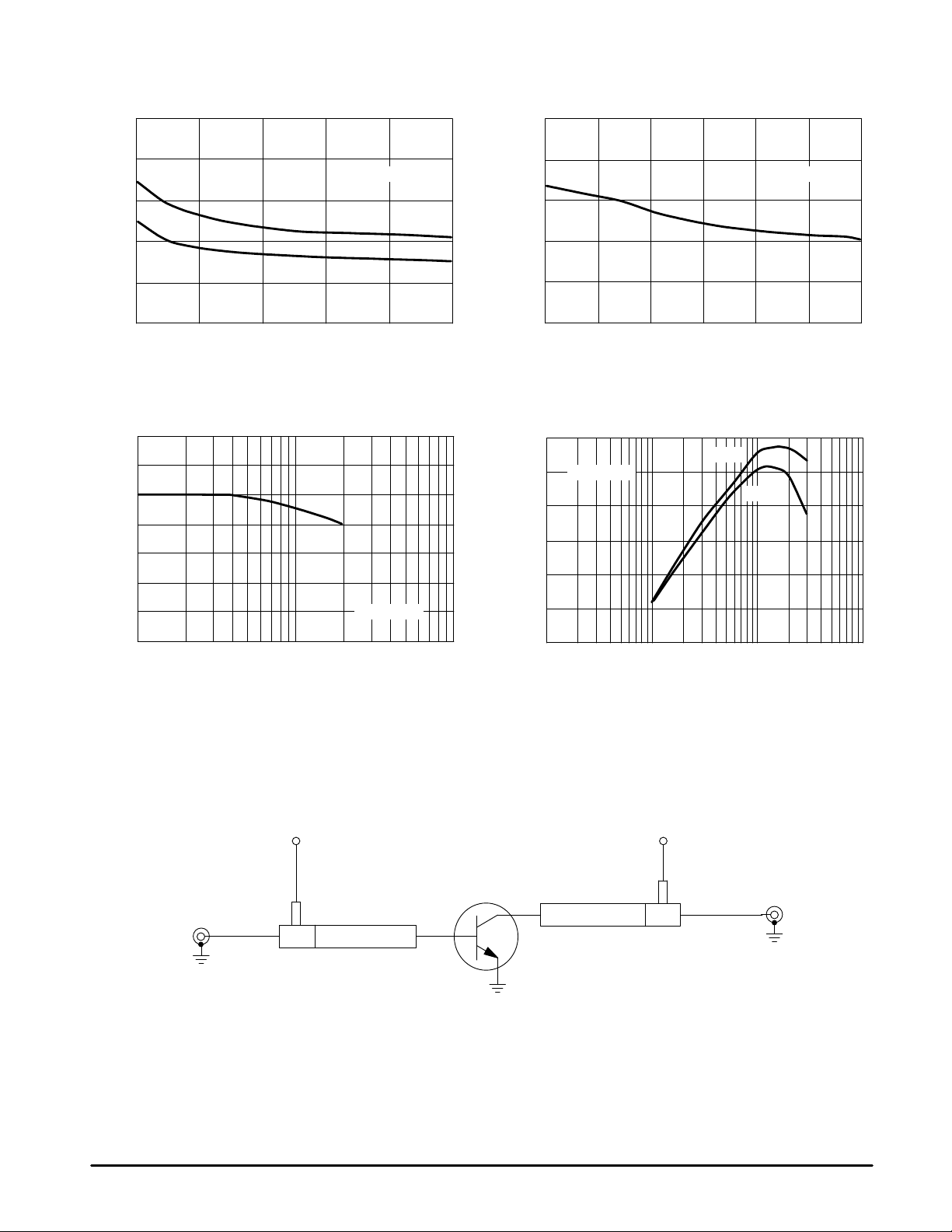
Figure 1. Capacitance
versus V oltage
C
ob
C
cb
0
VCB, REVERSE VOLTAGE
f = 1.0 MHz
108.06.04.02.00
, INPUT CAPACITANCE (pF)
IB
C
1.0
0.8
0.6
0.4
0.2
0
Figure 3. DC Current Gain
versus Collector Current
VCE = 1.0 V
10
IC, COLLECTOR CURRENT (mA)
1001.0 0.1
13
11
9.0
7.0
5.0
3.0
τ
f , GAIN BANDWIDTH PRODUCT (GHz)
1.0
Figure 2. Input Capacitance
versus V oltage
C
ib
0.25 0.75 1.25
VEB, EMITTER–BASE VOLTAGE
Figure 4. Gain–Bandwidth Product
versus Collector Current
3.0 V
f = 1.0 GHz
1.0 V
1.0
IC, COLLECTOR CURRENT (mA)
f = 1.0 MHz
1.51.00.50
10010
LIFETIME BUY
Figure 5. Functional Circuit Schematic
V
BE
RF Input
Network
MOTOROLA RF/IF DEVICE DATA
Slug TunerBias
Slug Tuner
V
CE
Bias
Network
RF Output
LAST ORDER: 25SEP01 LAST SHIP: 26MAR02
3
MRF1047T1
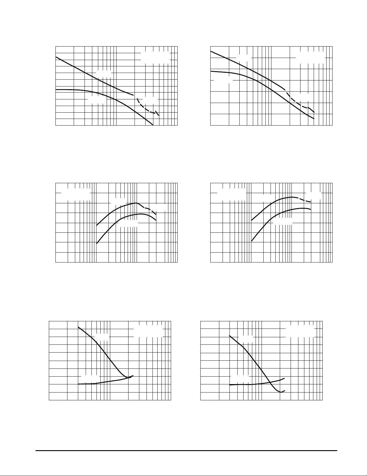
Figure 6. Maximum Stable/Available Gain and
Forward Insertion Gain versus Frequency
24
22
20
18
16
14
12
10
, FORWARD INSERTION GAIN (dB)
2
|
8.0
21
6.0
|S
4.0
2.0
0
MSG, MAXIMUM STABLE GAIN; MAG, MAXIMUM
0.1
AVAILABLE GAIN;
MSG
|S21|
f, FREQUENCY (GHz)
2
1.0 10 1.0 10
VCE = 1.0 V
IC = 1.0 mA
Figure 8. Maximum Stable/Available Gain and
Forward Insertion Gain versus Collector Current
20
VCE = 1.0 V
18
f = 1.0 GHz
16
14
12
, FORWARD INSERTION GAIN (dB)
2
10
|
21
8.0
MSG
|S21|
2
MAG
MAG
Figure 7. Maximum Stable/Available Gain and
Forward Insertion Gain versus Frequency
28
24
20
|S21|
16
12
, FORWARD INSERTION GAIN (dB)
2
|
21
8.0
4.0
0
MSG, MAXIMUM STABLE GAIN; MAG, MAXIMUM
0.1
AVAILABLE GAIN; |S
MSG
2
f, FREQUENCY (GHz)
VCE = 3.0 V
IC = 3.0 mA
MAG
Figure 9. Maximum Stable/Available Gain and
Forward Insertion Gain versus Collector Current
20
VCE = 3.0 V
18
f = 1.0 GHz
16
14
12
, FORWARD INSERTION GAIN (dB)
2
10
|
21
8.0
MSG
|S21|
2
MAG
6.0
4.0
MSG, MAXIMUM STABLE GAIN; MAG, MAXIMUM
AVAILABLE GAIN; |S
1.0 10 1.0 10
LIFETIME BUY
Figure 10. Minimum Noise Figure and
20
18
16
14
12
10
8.0
6.0
NF
4.0
G , ASSOCIATED GAIN (dB)
2.0
0
Associated Gain versus Frequency
VCE = 1.0 V
G
NF
NF
min
1.0 10 1.0 10
f, FREQUENCY (GHz)
IC = 1.0 mA
6.0
4.0
MSG, MAXIMUM STABLE GAIN; MAG, MAXIMUM
100 100
0.10.1
AVAILABLE GAIN; |S
IC, COLLECTOR CURRENT (mA)IC, COLLECTOR CURRENT (mA)
Figure 11. Minimum Noise Figure and
Associated Gain versus Frequency
5.0
4.0
3.0
2.0
1.0
0
26
22
18
14
, MINIMUM NOISE FIGURE (dB)
10
NF
min
G , ASSOCIATED GAIN (dB)
NF
6.0
0.10.1
G
NF
NF
min
f, FREQUENCY (GHz)
VCE = 3.0 V
IC = 3.0 mA
5.0
4.0
3.0
2.0
1.0
0
, MINIMUM NOISE FIGURE (dB)
min
NF
LAST ORDER: 25SEP01 LAST SHIP: 26MAR02
4
MOTOROLA RF/IF DEVICE DATA
 Loading...