Motorola MPIC2151D, MPIC2151P Datasheet

1
Motorola Power Products Division Advanced Data
Power Products Division
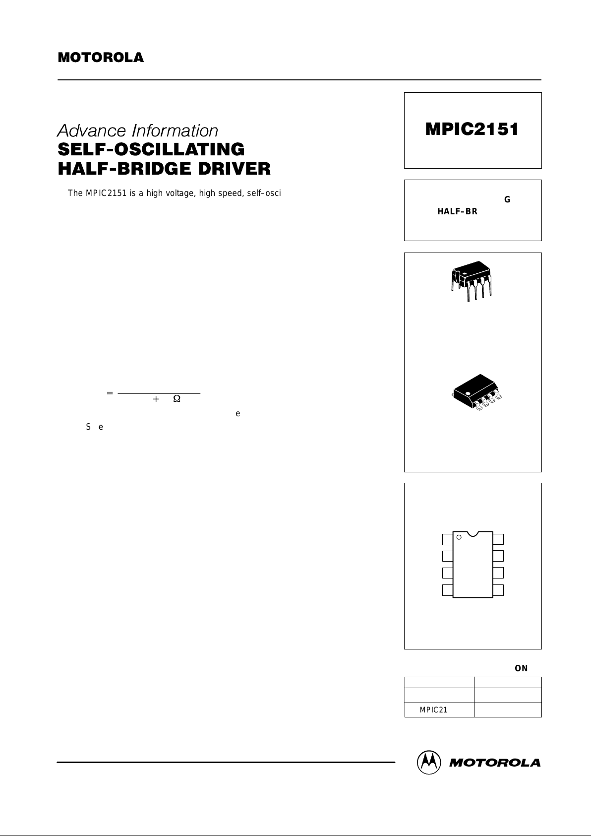
The MPIC2151 is a high voltage, high speed, self–oscillating power MOSFET
and IGBT driver with both high side and low side referenced output channels. Proprietary HVIC and latch immune CMOS technologies enable ruggedized monolithic construction. The front–end features a programmable oscillator which is similar
to the 555 timer. The output drivers feature a high pulse current buf fer stage and an
internal deadtime designed for minimum driver cross–conduction. Propagation delays for the two channels are matched to simplify use in 50% duty cycle applications. The floating channel can be used to drive an N–channel power MOSFET or
IGBT in the high side configuration that operates off a high voltage rail from 10 to
600 volts.
• Floating Channel Designed for Bootstrap Operation
• Fully Operational to +600 V
• Tolerant to Negative Transient Voltage
• dV/dt Immune
• Undervoltage Lockout
• Programmable Oscillator Frequency:
f
+
1
1.4 (RT)75W) CT
• Matched Propagation Delay for Both Channels
• Low Side Output In Phase with RT
PRODUCT SUMMARY
V
OFFSET 600 V MAX
Duty Cycle
50%
V
OUT 10 – 20 V
t
r/f
(typical) 120 & 60 ns
Deadtime (typical) 1.2 µs
This document contains information on a new product. Specifications and information herein are subject
to change without notice.
REV 1
Order this document
by MPIC2151/D
SEMICONDUCTOR TECHNICAL DATA
Device
Package
SELF–OSCILLATING
HALF–BRIDGE
DRIVER
ORDERING INFORMATION
MPIC2151P PDIP
D SUFFIX
PLASTIC PACKAGE
CASE 751–05
(SO–8)
8
1
(TOP VIEW)
PIN CONNECTIONS
P SUFFIX
PLASTIC PACKAGE
CASE 626–05
8
1
MPIC2151D SOIC
V
B
8V
CC
RT
CT
COM
HO
V
S
LO
7
6
5
1
2
3
4
Motorola, Inc. 1996

MPIC2151
2
Motorola Power Products Division Advanced Data
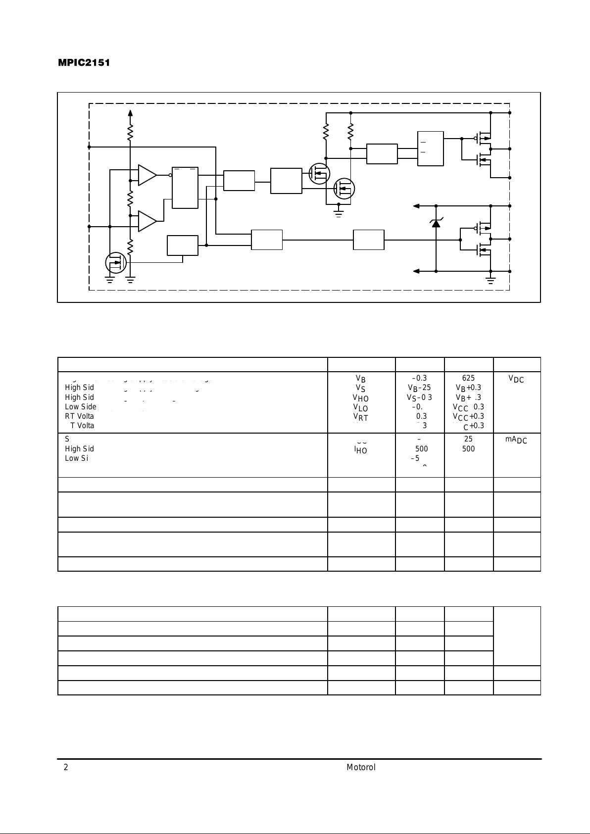
SIMPLIFIED BLOCK DIAGRAM
PULSE
GEN
PULSE
FILTER
HV
LEVEL
SHIFT
COM
LO
V
CC
V
S
V
B
HO
R
S
Q
DELAY
DEAD
TIME
DEAD
TIME
UV
DETECT
+
–
+
–
R
R
R
RT
CT
R
SQQ
15.6 V
ABSOLUTE MAXIMUM RATINGS
Absolute Maximum Ratings indicate sustained limits beyond which damage to the device may occur. All voltage parameters are absolute
voltages referenced to COM, all currents are defined positive into any lead. The Thermal Resistance and Power Dissipation ratings are
measured under board mounted and still air conditions.
Rating
Symbol Min Max Unit
High Side Floating Supply Absolute Voltage
V
–0.3
625
V
High Side Floating Supply Absolute Voltage
High Side Floating Supply Offset Voltage
V
B
V
–0.3
V
–25
625
V
+0.3
V
DC
High Side Floating Supply Offset Voltage
High Side Floating Output Voltage
V
S
V
HO
VB–25
VS–0.3
VB+0.3
VB+0.3
High Side Floating Output Voltage
Low Side Output Voltage
V
HO
V
LO
VS–0.3
–0.3
VB+0.3
VCC+0.3
Low Side Output Voltage
RT Voltage
V
LO
V
RT
–0.3
–0.3
VCC+0.3
VCC+0.3
CT Voltage
RT
V
CT
–0.3
CC
+0.3
VCC+0.3
Supply Current (Note 1) I
– 25 mA
Supply Current (Note 1)
High Side Output Current
I
CC
I
HO
–
–50025500
mA
DC
Low Side Output Current
HO
I
LO
–500
500
RT Output Current
IRT–5.0
5.0
Allowable Offset Supply Voltage Transient dVS/dt – 50 V/ns
*Package Power Dissipation @ TC ≤ +25°C (8 Lead DIP)
(8 Lead SOIC)
P
D
–
–
–
1.0
0.625
Watt
Operating and Storage Temperature Tj, T
stg
–55 150 °C
Thermal Resistance, Junction to Ambient (8 Lead DIP)
(8 Lead SOIC)
R
θJA
–
–
125
200
°C/W
Lead Temperature for Soldering Purposes, 10 seconds T
L
– 260 °C
RECOMMENDED OPERATING CONDITIONS
The Input/Output logic timing Diagram is shown in Figure 1. For proper operation the device should be used within the recommended conditions.
High Side Floating Supply Absolute Voltage
V
B
VS+10 VS+V
clamp
V
High Side Floating Supply Offset Voltage V
S
– 600
High Side Floating Output Voltage V
HO
V
S
V
B
Low Side Output Voltage V
LO
0 V
CC
Supply Current (Note 1) I
CC
– 5.0 mA
Ambient Temperature T
A
–40 125 °C
Note 1: Because the MPIC2151 is designed specifically for off–line supply systems, this IC contains a zener clamp structure between the chip
VCC and COM which has a nominal breakdown voltage of 15.6 V . Therefore, the IC supply voltage is normally derived by forcing current into
the supply lead (typically by means of a high value resistor connected between the chip VCC and the rectified line voltage and a local decoupling capacitor from VCC to COM) and allowing the internal zener clamp circuit to determine the nominal supply voltage. Therefore, this circuit
should not be driven by a DC, low impedance power source of greater than V
CLAMP
.
 Loading...