1
Motorola Power Products Division Advanced Data
Power Products Division
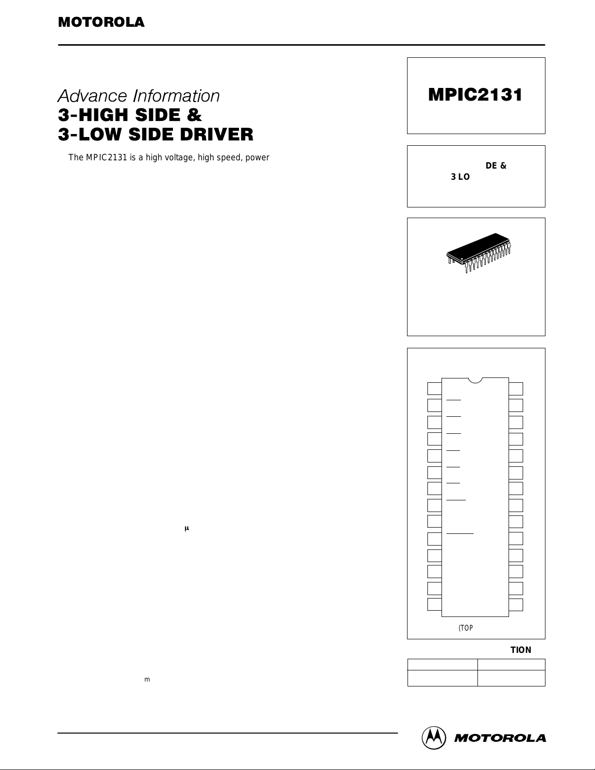
The MPIC2131 is a high voltage, high speed, power MOSFET and IGBT driver
with three independent high side and low side referenced output channels for
3–Phase applications. Proprietary HVIC technology enables ruggedized monolithic construction. Logic inputs are compatible with 5 V CMOS or LSTTL outputs. A
ground referenced operational amplifier provides an analog feedback of bridge
current via an external current sense resistor. A current trip function which terminates all six outputs is also derived from an external current sense resistor. An extra shutdown input is provided for customizing the shutdown function. An open
drain FAULT signal is provided to indicate that any of shutdown conditions has occurred. The output drivers feature a high pulse current buffer stage designed for
minimum driver cross–conduction. Propagation delays are matched to simplify use
in high frequency applications.
The floating channels can be used to drive N–channel power MOSFET or
IGBT’s in the high side configuration which operate from 10 to 600 volts.
• Floating Channel Designed for Bootstrap Operation
• Fully Operational to +600 V
• Tolerant to Negative Transient Voltage
• dV/dt Immune
• Gate Drive Supply Range from 10 to 20 V
• Undervoltage Lockout for All Channels
• Over–current Shut Down Turns Off All Six Drivers
• Independent 3 High Side & 3 Low Side Drivers
• Matched Propagation Delay for All Channels
• Outputs Out of Phase with Inputs
PRODUCT SUMMARY
V
OFFSET 600 V MAX
I
O+/– 200 mA/420 mA
V
OUT 10 – 20 V
t
on/off
(typical)
1.4 & 0.7 m
s
Delay Matching
700 ns
This document contains information on a new product. Specifications and information herein are subject
to change without notice.
REV 1
Order this document
by MPIC2131/D
SEMICONDUCTOR TECHNICAL DATA
Device
Package
3 HIGH SIDE &
3 LOW SIDE
DRIVER
ORDERING INFORMATION
(TOP VIEW)
PIN CONNECTIONS
P SUFFIX
PLASTIC PACKAGE
CASE 710–02
MPIC2131P PDIP
28
1
1
2
3
4
5
6
7
8
22
23
24
25
26
27
28
9
21
20
10
11
12
13
14
17
18
19
16
15
V
CC
HIN1
HIN2
HIN3
LIN1
LIN2
LIN3
FAULT
ITRIP
FLT+CLR
SD
V
SS
COM
LO3
V
B1
HO1
V
S1
V
B2
HO2
V
S2
V
B3
HO3
V
S3
LO1
LO2
Motorola, Inc. 1996

MPIC2131
2
Motorola Power Products Division Advanced Data
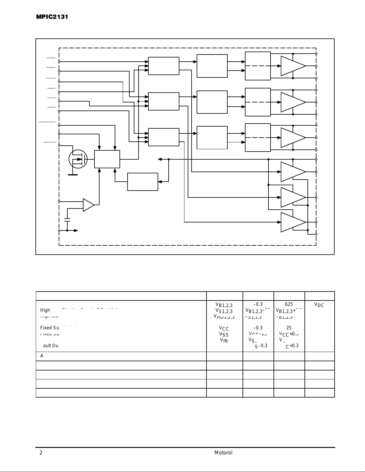
SIMPLIFIED BLOCK DIAGRAM
LATCH
UV
DETECTOR
DRIVER
PULSE
GENERATOR
LEVEL
SHIFTER
SET
RESET
LATCH
UV
DETECTOR
DRIVER
PULSE
GENERATOR
LEVEL
SHIFTER
SET
RESET
LATCH
UV
DETECTOR
DRIVER
SET
RESET
DRIVER
DRIVER
DRIVER
PULSE
GENERATOR
LEVEL
SHIFTER
INPUT
SIGNAL
GENERATOR
INPUT
SIGNAL
GENERATOR
INPUT
SIGNAL
GENERATOR
UNDER–
VOLTAGE
DETECTOR
FAULT
LOGIC
V
CC
V
B3
V
S2
V
S1
V
B1
HO1
H1
L1
H2
L2
H3
L3
CURRENT
COMPARATOR
V
B2
HO2
V
S3
LO1
LO2
LO3
COM
HIN1
HIN2
HIN3
LIN1
LIN2
LIN3
FLT–CLR
V
SS
ITRIP
HO3
0.5 V
SD
FAULT
V
SS
ABSOLUTE MAXIMUM RATINGS
Absolute Maximum Ratings indicate sustained limits beyond which damage to the device may occur. All voltage parameters are absolute
voltages referenced to COM. The Thermal Resistance and Power Dissipation ratings are measured under board mounted and still air
conditions.
Rating
Symbol Min Max Unit
High Side Floating Supply Offset Voltage
B1,2,3
V
S1,2,3
V
B1,2,3
–25
V
B1,2,3
+0.3
DC
High Side Floating Output Voltage
Low Side Output Voltage
V
HO1,2,3
V
LO1,2,3
V
S1,2,3
–0.3
–0.3
V
B1,2,3
+0.3
VCC+0.3
LO1,2,3
V
CC
CC
+0.3
25
Fixed Supply Offset Voltage
Logic Input Voltage (HIN–, LIN–, FLT–, CLR–, SD & ITRIP)
V
SS
V
IN
VCC–25
VSS–0.3
VCC+0.3
VCC+0.3
IN
FAULT
SS
–0.3
VSS–0.3
CC
+0.3
VCC+0.3
Allowable Offset Supply Voltage Transient dVS/dt – 50 V/ns
*Package Power Dissipation @ TC ≤ +25°C (28 Lead DIP) P
D
– 1.5 Watt
Operating and Storage Temperature Tj, T
stg
–55 150 °C
Thermal Resistance, Junction to Ambient (8 Lead DIP) R
θJA
– 83 °C/W
Lead Temperature for Soldering Purposes, 10 seconds T
L
– 260 °C
High Side Floating Absolute Voltage
Fixed Supply Voltage
Fault Output Voltage
V
B1,2,3
–0.3
–0.3
625
V
DC
 Loading...