

Motorola MPIC2117D, MPIC2117P Datasheet

1
Motorola Power Products Division Advanced Data
Power Products Division
The MPIC2117 is a high voltage, high speed, power MOSFET and IGBT driver.
Proprietary HVIC and latch immune CMOS technologies enable ruggedized monolithic construction. The logic input is compatible with standard CMOS outputs. The
output drivers feature a high pulse current buffer stage designed for minimum driver cross–conduction. The floating channel can be used to drive an N–channel power MOSFET or IGBT in the high side or low side configuration which operates from
10 to 600 volts.
• Floating Channel Designed for Bootstrap Operation
• Fully Operational to +600 V
• Tolerant to Negative Transient Voltage
• dV/dt Immune
• Gate Drive Supply Range from 10 to 20 V
• Undervoltage Lockout
• CMOS Schmitt–triggered Input with Pull–down
• Output In Phase with Input
PRODUCT SUMMARY
V
OFFSET 600 V MAX
I
O+/– 200 mA/420 mA
V
OUT 10 – 20 V
t
on/off
(typical)
125 & 105 ns
V
B
8V
CC
IN
COM
HO
V
S
7
6
5
1
2
3
4
V
B
8V
CC
IN
COM
HO
V
S
7
6
5
1
2
3
4
8 LEADS DIP
MPIC2117P
8 LEAD SOIC
MPIC2117D
PIN CONNECTIONS
(TOP VIEW)
This document contains information on a new product. Specifications and information herein are subject
to change without notice.
REV 1
Order this document
by MPIC2117/D
SEMICONDUCTOR TECHNICAL DATA
Device
Package
SINGLE CHANNEL DRIVER
ORDERING INFORMATION
MPIC2117P PDIP
D SUFFIX
PLASTIC PACKAGE
CASE 751–05
(SO–8)
8
1
P SUFFIX
PLASTIC PACKAGE
CASE 626–05
8
1
MPIC2117D SOIC
Motorola, Inc. 1996
MPIC2117
2
Motorola Power Products Division Advanced Data
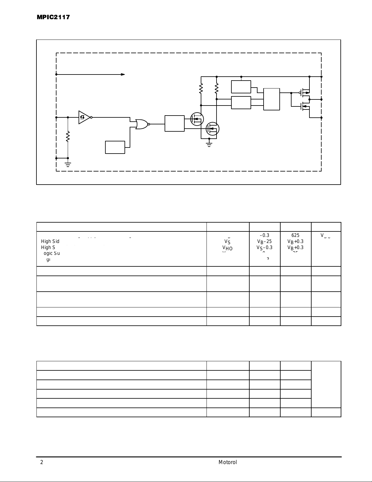
SIMPLIFIED BLOCK DIAGRAM
PULSE
GEN
UV
DETECT
PULSE
FILTER
HV
LEVEL
SHIFT
V
S
V
B
HO
R
R
S
Q
V
CC
IN
COM
UV
DETECT
ABSOLUTE MAXIMUM RATINGS
Absolute Maximum Ratings indicate sustained limits beyond which damage to the device may occur. All voltage parameters are absolute
voltages referenced to COM. The Thermal Resistance and Power Dissipation ratings are measured under board mounted and still air
conditions.
Rating
Symbol Min Max Unit
High Side Floating Supply Absolute Voltage
High Side Floating Supply Offset Voltage
V
B
V
S
–0.3
VB–25
625
VB+0.3
V
DC
S
V
HO
B
–25
VS–0.3
B
+0.3
VB+0.3
Logic Supply Voltage
VCC–0.3
25
Logic Input Voltage
VIN–0.3
VCC+0.3
Allowable Offset Supply Voltage Transient dVS/dt – 50 V/ns
*Package Power Dissipation @ TA ≤ +25°C (8 Lead DIP)
(8 Lead SOIC)
P
D
–
–
–
1.0
0.625
Watt
Thermal Resistance, Junction to Ambient (8 Lead DIP)
(8 Lead SOIC)
R
θJA
–
–
125
200
°C/W
Operating and Storage Temperature Tj, T
stg
–55 150 °C
Lead Temperature for Soldering Purposes, 10 seconds T
L
– 260 °C
RECOMMENDED OPERATING CONDITIONS
The Input/Output logic timing Diagram is shown in Figure 1. For proper operation the device should be used within the recommended conditions. The VS offset rating is tested with all supplies biased at 15 V differential.
High Side Floating Supply Absolute Voltage
V
B
VS+10 VS+20
High Side Floating Supply Offset Voltage V
S
Note 1 600
High Side Floating Output Voltage V
HO
V
S
V
B
Logic Supply Voltage V
CC
10 20
Logic Input Voltage V
IN
0 V
CC
Ambient Temperature T
A
–40 125 °C
Note 1: Logic operational for VS of –5 to +600 V. Logic state held for VS of –5 V to –VBS.
High Side Floating Supply Absolute Voltage V
High Side Floating Output Voltage
–0.3 625 V
V
 Loading...