Motorola MPC993FA Datasheet

SEMICONDUCTOR TECHNICAL DATA
1
REV 0
Motorola, Inc. 1997
9/97
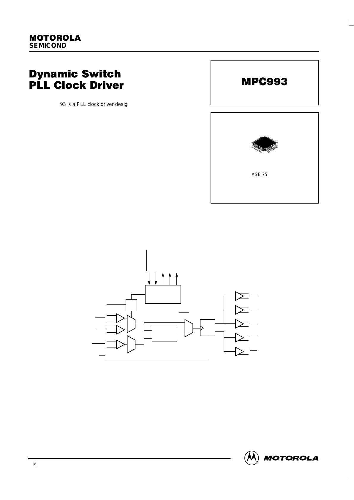
The MPC993 is a PLL clock driver designed specifically for redundant
clock tree designs. The device receives two differential LVPECL clock
signals from which it generates 5 new differential LVPECL clock outputs.
Two of the output pairs regenerate the input signals frequency and phase
while the other three pairs generate 2x, phase aligned clock outputs.
External PLL feedback is used to also provide zero delay buffer
performance.
• Fully Integrated PLL
• Intelligent Dynamic Clock Switch
• LVPECL Clock Outputs
• LVCMOS Control/Statis I/O
• 3.3V Operation
• 32–Lead TQFP Packaging
• ±50ps Cycle–Cycle Jitter
The MPC993 continuously monitors the two input signals to identify faulty reference clocks. Upon identification of a faulty
input clock (input clock stuck HIGH or LOW for at least 3 feedback clock edges), an input bad flag will be set and the device will
automatically switch from the bad reference clock input to the good one. During this dynamic switch of the input references, the
MPC993 outputs will slew, with minimal period disturbances to the new phase.
Figure 1. Block Diagram
CLK0
CLK0
CLK1
CLK1
Ext_FB
Ext_FB
OR
Sel_Clk
Dynamic Switch
Logic
PLL
PLL_En
÷
2
÷
4
Qb0
Qb0
Qb1
Qb1
Qb2
Qb2
Qa0
Qa0
Qa1
Qa1
MR
Man_OVerride
Alarm_Reset
Inp0bad
Inp1bad
Clk_Selected
FA SUFFIX
32–LEAD PLASTIC TQFP PACKAGE
CASE 751D–04

MPC993
MOTOROLA ECLinPS and ECLinPS Lite
DL140 — Rev 3
2
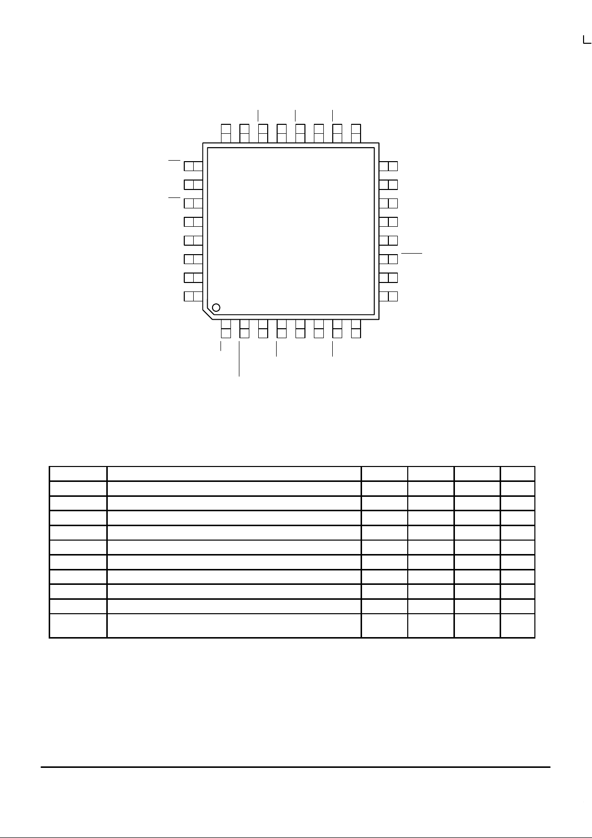
Figure 2. 32–Lead Pinout (Top View)
GND
VCC
Qb0
Qb0
Qb1
Qb1
Qb2
Qb2
VCC
MR
Alarm_Reset
CLK0
CLK0
Sel_Clk
CLK1
CLK1
GNDA
25
26
27
28
29
30
31
32
15
14
13
12
11
10
9
12345678
24 23 22 21 20 19 18 17
16
PRELIMINARY
MPC993
Ext_FB
Ext_FB
GND
Clk_Selected
Inp1bad
Inp0bad
VCC
PLL_En
Man_Override
VCCA
VCC
Qa0
Qa0
Qa1
Qa1
3.3V PECL DC Characteristics (TA = 0°C to 70°C)
Symbol Parameter Min Typ Max Unit
V
OH
Output HIGH Voltage (LVPECL Outputs) 2.275 2.345 2.420 V
V
OH
Output HIGH Voltage (LVCMOS Outputs) 2.4 V
V
OL
Output LOW Voltage (LVPECL Outputs) 1.490 1.595 1.680 V
V
OL
Output LOW Voltage (LVCMOS Outputs) 0.5 V
V
IH
Input HIGH Voltage (LVPECL Outputs) 2.135 2.420 V
V
IH
Input HIGH Voltage (LVCMOS Outputs) 2.0 3.3 V
V
IL
Input LOW Voltage (LVPECL Outputs) 1.490 1.825 V
V
IL
Input LOW Voltage (LVCMOS Outputs) 0.8 V
I
IL
Input LOW Current 0.5 µA
I
EE
Power Supply Current GNDA
GND
15
80
mA
 Loading...