SEMICONDUCTOR TECHNICAL DATA
1
REV 1
Motorola, Inc. 1996
7/96
The MPC992 is a 3.3V compatible, PLL based PECL clock generator
and distributor. The fully differential design ensures optimum skew and
PLL jitter performance. The performance of the device makes the
MPC992 ideal for workstations, main frame computer, telecommunication
and instrumentation applications. The device offers a crystal oscillator or
a differential PECL reference clock input to provide flexibility in the
reference clock interface. All of the control signals to the MPC992 are
LVTTL compatible inputs.
• Fully Integrated PLL
• Output Frequency of up to 400MHz
• PECL Clock Inputs and Outputs
• Operates from a 3.3V V
CC
Supply
• Output Frequency Configurable
• 32 TQFP Packaging
• ±25ps Cycle–Cycle Jitter
The MPC992 offers two banks of outputs which can be configured into
four different relationships. The output banks can be configured into 2:1,
3:1, 3:2 and 5:2 ratios to provide a wide variety of potential frequency
outputs. In addition to these two banks of outputs a synchronization output is also offered. The SYNC output will provide
information as to the time when the two output banks will transition positively in phase. This information can be important when
the odd ratios are used as it provides for a baseline point in the system timing. The SYNC output will pulse high for one Qa clock
period, centered on the rising Qa clock edge four edges prior to the Qb synchronous edge. The relationship is illustrated in the
timing diagrams in the data sheet.
The MPC992 offers several features to aid in system debug and test. The PECL reference input pins can be interfaced to a test
signal and the PLL can be bypassed to allow the designer to drive the MPC992 outputs directly. This allows for single stepping in
a system functional debug mode. In addition an overriding reset is provided which will force all of the Q outputs LOW upon
assertion.
The MPC992 is packaged in a 32–lead TQFP package to optimize both performance and board density.
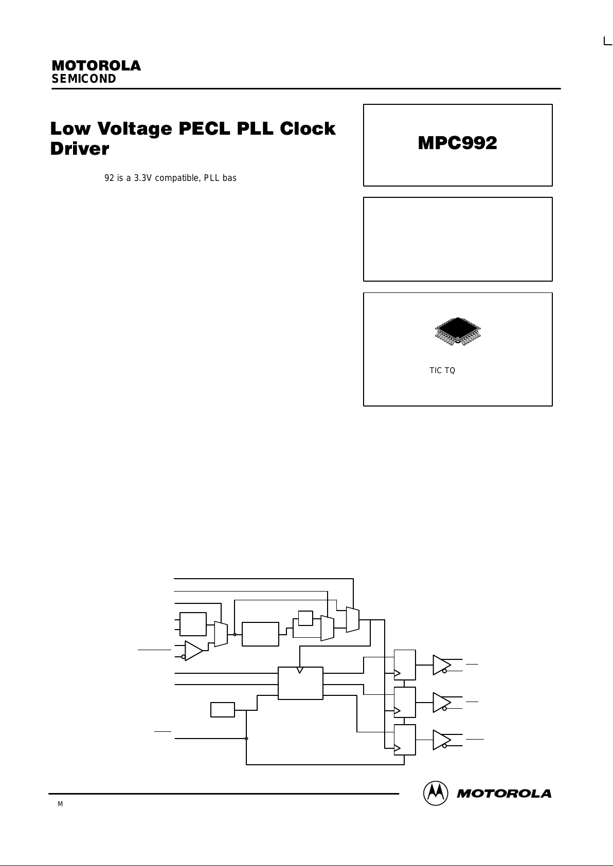
Qan
Qan
(x4)
Qbn
Qbn
(x3)
SYNC
SYNC
(x1)
Frequency
Generator
PLL_EN
PECL_CLK
PECL_CLK
XTAL_SEL
XTAL
OSC
XTAL1
XTAL2
VCO_SEL
Integrated
PLL
x2
FSEL0
FSEL1
POR
Reset
MPC992 LOGIC DIAGRAM
1
0
0
1
0
1
LOW VOLTAGE
PLL CLOCK DRIVER
FA SUFFIX
PLASTIC TQFP PACKAGE
CASE 873A-02

MPC992
MOTOROLA TIMING SOLUTIONS
BR1333 — REV 5
2
Qb1
Qb2
Qa1
Qa1
Qa0
GNDA
VCCA
VCCI
Qb0
Qb1
Qb2
PLL_EN
GNDI
VCCO1
Qa2
Qa2
Qa3
Qa3
SYNC
SYNC
VCCO2
VCO_SEL
FSEL0
FSEL1
XTAL_SEL
PECL_CLK
PECL_CLK
XTAL1
XTAL2
25
26
27
28
29
30
31
32
15
14
13
12
11
10
9
12345678
24 23 22 21 20 19 18 17
16
MPC992
Reset
Qa0
Qb0
FUNCTION TABLE 1
FSEL0 FSEL1 Qa Qb Feedback Ratio
0
0
1
1
0
1
0
1
VCO/4
VCO/2
VCO/4
VCO/2
VCO/6
VCO/4
VCO/10
VCO/6
VCO/24
VCO/16
VCO/40
VCO/24
3:2
2:1
5:2
3:1
INPUT vs OUTPUT FREQUENCY
FSEL0 FSEL1 Qa Qb Int Feedback
0
0
1
1
0
1
0
1
6 (f
ref
)
8 (f
ref
)
10 (f
ref
)
12 (f
ref
)
4 (f
ref
)
4 (f
ref
)
4 (f
ref
)
4 (f
ref
)
f
ref
f
ref
f
ref
f
ref
FUNCTION TABLE 2
Control Signal Logic ‘0’ Logic ‘1’
Reset Outputs Enabled Outputs Disabled
XTAL_SEL PECL REF XTAL REF
PLL_EN Disabled Enabled
VCO_SEL High Frequency Low Frequency
PIN DESCRIPTION
Pin Name Function
VCO_SEL VCO range select pin (Int Pullup)
PLL_EN PLL bypass select pin (Int Pullup)
XTAL_SEL Input reference source select pin (Int Pullup)
XTAL1:2 Crystal interface pins for the internal oscillator
PECL_CLK True PECL reference clock input (Int Pulldown)
PECL_CLK
Compliment PECL reference clock input
(Int Pullup)
FSELn Internal divider select pins (Int Pullup)
RESET
Internal flip–flop reset, true outputs go LOW
(Int Pulldown)

MPC992
TIMING SOLUTIONS
BR1333 — REV 5
3 MOTOROLA
Figure 1. Output Waveforms
Qa
2:1 Mode
Qb
SYNC
Qa
3:1 Mode
Qb
SYNC
Qa
3:2 Mode
Qb
SYNC
5:2 Mode
Qa
Qb
SYNC
ABSOLUTE MAXIMUM RATINGS*
Symbol Parameter Min Max Unit
V
CC
Supply Voltage –0.3 4.6 V
V
I
Input Voltage –0.3 VDD + 0.3 V
I
OUT
Output Current Continuous
Surge
50
100
mA
T
Stor
Storage Temperature Range –40 125 °C
* Absolute maximum continuous ratings are those values beyond which damage to the device may occur. Exposure to these conditions or
conditions beyond those indicated may adversely affect device reliability. Functional operation under absolute-maximum-rated conditions is not
implied.
 Loading...