

Motorola MPC990FA, MPC991FA Datasheet
SEMICONDUCTOR TECHNICAL DATA
1
REV 2
Motorola, Inc. 1997
2/97
The MPC990/991 is a 3.3V compatible, PLL based ECL/PECL clock
driver. The fully differential design ensures optimum skew and PLL jitter
performance. The performance of the MPC990/991 makes the device
ideal for Workstation, Mainframe Computer and Telecommunication
applications. The MPC990 and MPC991 devices are identical except in
the interface to the reference clock for the PLL. The MPC990 offers an
on–board crystal oscillator as the PLL reference while the MPC991 offers
a differential ECL/PECL input for applications which need to lock to an
existing clock signal. Both designs offer a secondary single–ended ECL
clock for system test capabilities.
• Fully Integrated PLL
• Output Frequency Up to 400MHz
• ECL/PECL Inputs and Outputs
• Operates from a 3.3V Supply
• Output Frequency Configurable
• TQFP Packaging
• ±50ps Cycle–to–Cycle Jitter
The MPC990/991 offers three banks of outputs which can each be
programmed via the the four fsel pins of the device. There are 16 different
output frequency configurations available in the device. The
configurations include output ratios of 1:1, 2:1, 3:1, 3:2, 4:1, 4:3, 4:3:1 and
4:3:2. The programming table in this data sheet illustrates the various
programming options. The SYNC output monitors the relationship
between the Qa and Qc output banks. The output pulses per the timing
diagrams in this data sheet signal the coincident edges of the two output
banks. This feature is useful for non binary relationships between output frequencies (i.e., 3:2 or 4:3 relationships). The Sync_Sel
input toggles the Qd outputs between sync signals and extensions to the Qc bank of outputs.
The MPC990/991 provides a separate output for the feedback to the PLL. This allows for the feedback frequency to be
programmed independently of the other outputs allowing for unique input vs output frequency relationships. The fselFB inputs
provide 6 different feedback frequencies from the QFB differential output pair.
The MPC990/991 features an external differential ECL/PECL feedback to the PLL. This external feedback feature allows for
the MPC991’s use as a “zero” delay buffer. The propagation delay between the input reference and the output is dependent on
the input reference frequency. The selection of higher reference frequencies will provide near zero delay through the device.
The PLL_En, Ref_Sel and the Test_Clk input pins provide a means of bypassing the PLL and driving the output buffers
directly. This allows the user to single step a design during system debug. Note that the Test_Clk input is routed through the
dividers so that depending on the programming several edges on the Test_Clk input will be needed to get corresponding edge
transitions on the outputs. The VCO_Sel input provides a means of recentering the VCO to provide a broader range of VCO
frequencies for stable PLL operation.
If the frequency select or the VCO_Sel pins are changed during operation, a master reset signal must be applied to ensure
output synchronization and phase–lock. If the VCO is driven beyond its maximum frequency, the VCO can outrun the internal
dividers when the VCO_Sel pin is low. This will also prevent the PLL from achieving lock. Again, a master reset signal will need to
be applied to allow for phase–lock. The device employs a power–on reset circuit which will ensure output synchronization and
PLL lock on initial power–up.
LOW VOLTAGE
PLL CLOCK DRIVER
FA SUFFIX
52–LEAD TQFP PACKAGE
CASE 848D–03

MPC990 MPC991
MOTOROLA TIMING SOLUTIONS
BR1333 — Rev 6
2
QFB
QFB
VCCO
Qd0
Qd0
Qd1
Qd1
VCCO
Qc0
Qc0
Qc1
Qc1
VCCA
fsel0
Qb2
Qb2
fsel1
Qb1
Qb1
fsel2
Qb0
Qb0
VCCO
Qc2
Qc2
fsel3
GNDI
MR
PLL_En
Ref_Sel
fselFB2
fselFB1
fselFB0
Test_Clk
VCCI
Ext_FB
xtal1 (990)
xtal2 (990)
Ext_FB
40
41
42
43
44
45
46
47
48
49
50
51
52
25
24
23
22
21
20
19
18
17
16
15
14
12345678910111213
39 38 37 36 35 34 33 32 31 30 29 28 27
26
MPC990/
MPC991
ECL_CLK (991)
ECL_CLK (991)
VCO_Sel
SYNC_Sel
Qa3
Qa3
Qa2
Qa2
Qa1
Qa1
Qa0
Qa0
VCCO
Qb3
Qb3
Figure 1. 52–Lead Pinout (Top View)
FUNCTION TABLE 1
INPUTS OUTPUTS
fsel3 fsel2 fsel1 fsel0 Qa Qb Qc
0 0 0 0 ÷2 ÷2 ÷2
0 0 0 1 ÷2 ÷2 ÷4
0 0 1 0 ÷2 ÷4 ÷4
0 0 1 1 ÷2 ÷2 ÷6
0 1 0 0 ÷2 ÷6 ÷6
0 1 0 1 ÷2 ÷4 ÷6
0 1 1 0 ÷2 ÷4 ÷8
0 1 1 1 ÷2 ÷6 ÷8
1 0 0 0 ÷2 ÷2 ÷8
1 0 0 1 ÷2 ÷8 ÷8
1 0 1 0 ÷4 ÷4 ÷6
1 0 1 1 ÷4 ÷6 ÷6
1 1 0 0 ÷4 ÷6 ÷8
1 1 0 1 ÷6 ÷6 ÷8
1 1 1 0 ÷6 ÷8 ÷8
1 1 1 1 ÷8 ÷8 ÷8
MPC990 MPC991
TIMING SOLUTIONS
BR1333 — Rev 6
3 MOTOROLA
FUNCTION TABLE 2
fselFB2 fselFB1 fselFB0 QFB
0
0
0
0
0
0
1
1
0
1
0
1
÷2
÷4
÷6
÷8
1
1
1
1
0
0
1
1
0
1
0
1
÷8
÷16
÷24
÷32
FUNCTION TABLE 3
Control Pin Logic ‘0’ Logic ‘1’
PLL_En Enable PLL Bypass PLL
VCO_Sel fVCO fVCO/2
Ref_Sel xtal or ECL/PECL Test_Clk
MR — Reset Outputs
SYNC_Sel SYNC Outputs Match Qc Outputs
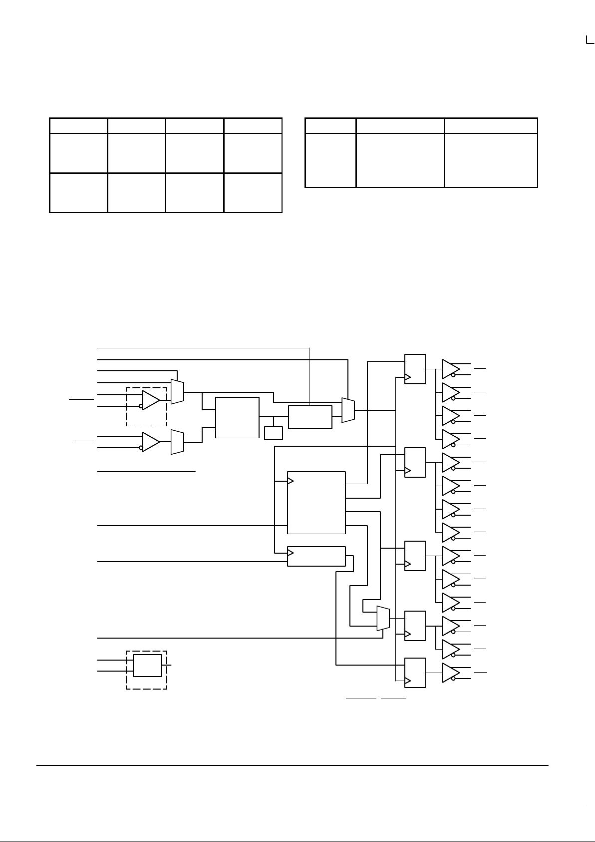
Figure 2. MPC990/991 Logic Diagram
VCO
PHASE
DETECTOR
LPF
PLL_En
VCO_Sel
ECL_Clk
ECL_Clk
Test_Clk
Ref_Sel
Ext_FB
Ext_FB
Qa0
Qa0
Qa1
Qa1
Qa2
Qa2
Qa3
Qa3
Qb0
Qb0
Qb1
Qb1
Qb2
Qb2
Qb3
Qb3
Qc0
Qc0
Qc1
Qc1
Qc2
Qc2
Qd0
Qd0
Qd1
Qd1
QFB
QFB
FREQUENCY
GENERATOR
SYNC
MR
fsela0:3
fselFB0:2
SYNC_Sel
(Pulldown)
(Pulldown)
(Pulldown)
(Pulldown)
(Pulldown)
(Pulldown)
(Pulldown)
(Pulldown)
MPC991
MPC990
Xtal
Osc
NOTE: ECL_Clk, Ext_FB have internal pulldowns, while ECL_Clk, Ext_FB have external
pullups to ensure stability under open input conditions.
 Loading...