


Motorola MPC980FA Datasheet
SEMICONDUCTOR TECHNICAL DATA
1
REV 2
Motorola, Inc. 1998
1/98
The MPC980 is a 3.3V dual PLL clock generator targeted for high end
Pentium and PowerPC 603/604 personal computers. The MPC980
synthesizes processor as well as PCI clocks from a 14.31818MHz
external crystal. In addition the device provides two buffered outputs of
the 14.31818MHz crystal as well as a 40MHz SCSI clock, a 24MHz floppy
clock and a 12MHz keyboard clock. One of the buffered 14.31818MHz
outputs can be configured to provide a 16MHz output rather than the
second copy of the 14.31818MHz output.
• Provides Processor and System Clocks for Pentium Designs
• Provides Processor and System Clocks for PowerPC 603/604
Designs
• Two Fully Integrated Phase–Locked Loops
• Cycle–to–Cycle Jitter of ±150ps
• Operates from 3.3V Supply
• 52–Lead LQFP Packaging
The processor clock outputs of the MPC980 can be programmed to
provide 50, 60 or 66MHz. Under all processor output frequencies the PCI
clock outputs will be equal to one half the processor clock outputs. The
PCI outputs will run synchronously to the processor clock outputs. There
are a total of ten output clocks which can be split into a group of four and a
group of six. Either group can be configured as processor or PCI clocks.
Each of the outputs can drive two series terminated transmission lines
allowing for the driving of up to twelve independent processor loads and
eight PCI clock loads. A pin selectable option is available to delay the PCI
clock outputs relative to the processor clocks. The amount of delay is a
function of the processor clock frequency and varies from 2ns to 6ns.
The output jitter of the the PLL at 66MHz output is ±150ps peak–to–peak, cycle–to–cycle (the worst case deviation of the clock
period is guaranteed to be less than ±150ps). The skews between one processor clock and any other processor clock (or one
PCI clock to any other PCI clock) is 350ps. The worst case skew between the processor clocks and the PCI clocks is 500ps.
An output enable pin is provided to tristate all of the outputs for board level test. In addition a testing mode is provided to allow
for the bypass of the PLL’s for board level functional debug.
Pentium is a trademark of Intel Corporation. PowerPC is a trademark of International Business
Machines Corporation.
DUAL 3.3V PLL
CLOCK GENERATOR
FA SUFFIX
52–LEAD LQFP PACKAGE
CASE 848D–03
MPC980
MOTOROLA ECLinPS and ECLinPS Lite
DL140 — Rev 3
2
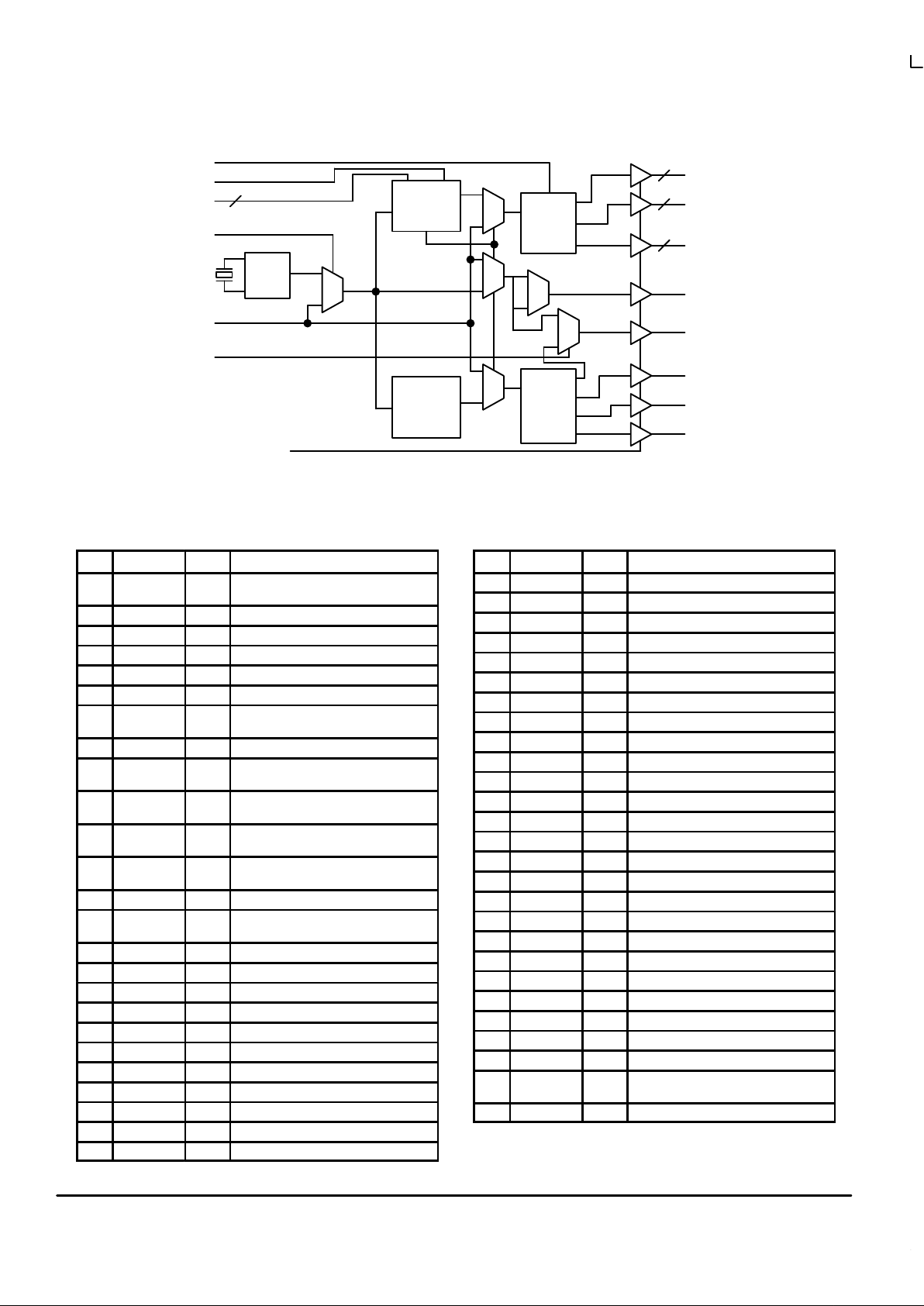
Figure 1. Logic Diagram
Processor
Clock PLL
Test Mode
Xtal
Osc
14.31818MHz
fsel0:1
Dly_PCI
÷
2
÷2/÷
4
÷
4
2
QP0:3
4
QP4:5_QPCI4:5
2
QPCI0:3
4
Q14.3M
Q14_16M
16MHz
12MHz
16M_Sel
Q12M
Q24M
Q40M
24MHz
40MHz
System
Clock PLL
TCLK
OE
0
1
0
1
TCLK_Sel
fsel2
Table 1. Pin Descriptions
Pin Label Ω Description
1 VCCA Analog VCC for System PLL Use
Filter
(Note 1.)
2 TCLK_Sel ↓ 50K Sel Ext’l TCLK or Internal Xtal Ref
3 TCLK None External LVCMOS Ref Signal
4 Xtal1 None Xtal Pin 1
5 Xtal2 None Xtal Pin 2
6 GND System Ground Input
7 DLY_PCI ↓ 50K Sets QP & QPI Relationship
(See Function Table 2 on page 3.)
8 VCCI VCC Pin for Internal Circuits
9 fsel0 ↑ 50K Least Bit for QP/QPI Output Funct
(See Function Table 1 on page 3.)
10 fsel1 ↓ 50K Most Bit for QP/QPI Output Function
(See Function Table 1 on page 3.)
11 fsel2 ↓ 50K Selection of QP/QPI Output Funct
(See Function Table 4 on page 3.)
12 VCCA Analog VCC Proc’ssr PLL Use Filter
(Note 1.)
13 GNDA System Ground Input
14 16M_SEL ↓ 50K Selects 16MHz / 14MHz for
Q14_16M Output
15 Q14_16M Output for 16MHz / 14MHz Xtal Osc
16 GND0 System Ground Input
17 VCC0 VCC in for the CMOS Outputs
18 Q14M CMOS Output for 14.3MHz Xtal Osc
19 GND0 System Ground Input
20 QP0 CMOS Output QP0
21 VCC0 VCC in for the CMOS Outputs
22 QP1 CMOS Output QP1
23 GND0 System Ground Input
24 QP2 CMOS Output QP2
25 VCC0 VCC in for the CMOS Outputs
Pin Label Ω Description
26 GNDI System Ground Input
27 VCCO VCC in for the CMOS Outputs
28 QP3 CMOS Output QP3
29 GND0 System Ground Input
30 GND0 System Ground Input
31 QP4_PCI4 CMOS Output QP4_PCI4
32 VCC0 VCC in for the CMOS Outputs
33 QP5_PCI5 CMOS Output QP5_PCI5
34 GND0 System Ground Input
35 GND0 System Ground Input
36 QPCI3 CMOS Output QPCI3
37 VCCO VCC in for the CMOS Outputs
38 QPCI2 CMOS Output QPCI2
39 GND0 System Ground Input
40 VCCI VCC for Internal Core Logic
41 GND0 System Ground Input
42 QPCI1 CMOS Output QPCI1
43 VCC0 VCC in for the CMOS Outputs
44 QPCI0 CMOS Output QPCI0
45 GND0 System Ground Input
46 QM12 CMOS Output QM12
47 VCC0 VCC in for the CMOS Outputs
48 Q40M CMOS Output Q40M
49 GND0 System Ground Input
50 Q24M CMOS Output Q24M
51 OE ↑ 50K Select Output State
(See Function Table 1 on page 3.)
52 GND0 System Ground Input
1. The filter recommended for the analog power pins is found in
Figure 3 in the Applications Information section on page 5.
MPC980
ECLinPS and ECLinPS Lite
DL140 — Rev 3
3 MOTOROLA
Figure 2. 52–Lead Pinout (Top View)
VCCI
GND0
QPCI1
VCC0
QPCI0
GND0
Q12M
VCC0
Q40M
GND0
Q24M
OE
GNDA
GNDI
VCC0
QP2
GND0
QP1
VCC0
QP0
GND0
Q14M
VCC0
GND0
Q14_16M
16M_Sel
GND0
QPCI2
VCC0
QPCI3
GND0
GND0
QP5_PCI5
VCC0
QP4_PCI4
GND0
GND0
QP3
VCC0
TCLK_Sel
VCCA
TCLK
Xtal1
Xtal2
GND
Dly_PCI
VCCI
fsel0
fsel1
fsel2
VCCA
GNDA
40
41
42
43
44
45
46
47
48
49
50
51
52
25
24
23
22
21
20
19
18
17
16
15
14
12345678910111213
39 38 37 36 35 34 33 32 31 30 29 28 27
26
MPC980
Function Table 1
OE fsel0 fsel1 QP QPCI Q14M Q16M Q24M Q12M Q40M
0 X X High Impedance High Impedance Hi Z Hi Z Hi Z Hi Z Hi Z
1 0 0 50MHz 25MHz 14.31818 16 24 12 40
1 0 1 60MHz 30MHz 14.31818 16 24 12 40
1 1 0 66MHz 33MHz 14.31818 16 24 12 40
1 1 1 TCLK/2 TCLK/4 TCLK TCLK/6 TCLK/4 TCLK/8 TCLK/2
Function Table 2
Dly_PCI QP/QPCI Relationship
0
1
Synchronous Processor & PCI Clocks
PCI Clocks Lag Processor Clocks
Function Table 3
TCLK_Sel PLL Input Reference
0
1
Crystal Oscillator
TCLK
Function Table 4
fsel2 QP/QPCI Output Configuration
0
1
6 Processor and 4 PCI Clocks
4 Processor and 6 PCI Clocks
Function Table 5
16M_Sel Q14_16M Output Configuration
0
1
14.31818MHz to Q14_16M Out
16MHz to Q14_16M Out