Motorola MPC974FA Datasheet

SEMICONDUCTOR TECHNICAL DATA
1
REV 2
Motorola, Inc. 1997
1/97
The MPC974 is a fully integrated PLL based clock generator and clock
distribution chip which operates from a 3.3V supply. The MPC974 is
ideally suited for high speed, timing critical designs which need a high
level of clock fanout. The device features 15 high drive LVCMOS outputs,
each output has the capability of driving a 50Ω parallel terminated
transmission line or two 50Ω series terminated transmission lines on the
incident edge.
• Fully Integrated PLL
• Two Reference Clock Inputs for Redundant Clock Applications
• High Impedance Output Control
• Logic Enable on the Outputs
• 3.3V V
CC
Supply
• Output Frequency Configurable
• TQFP Packaging
• ±100ps Typical Cycle–to–Cycle Jitter
The MPC974 features 3 independent frequency programmable banks
of outputs. The frequency programmability offers the capability of
establishing output frequency relationships of 1:1, 2:1, 3:1, 3:2 and 3:2:1.
In addition, the device features a separate feedback output which allows
for a wide variety of input/output frequency multiplication alternatives.
The VCO_Sel pin provides an extended VCO lock range for added
flexibility and general purpose usage.
The TCLK0 and TCLK1 inputs provide a method for dynamically
switching the PLL between two different clock sources. The PLL has been
optimized to provide small deviations in output pulse width and well
controlled, slow transition back to lock when the inputs are switched
between two references that are equal in frequency but out of phase with
each other. This feature makes the MPC974 an ideal solution for fault
tolerant applications which require redundant clock sources.
All of the control pins are LVTTL/LVCMOS level inputs. The Fsel pins control the VCO divide ratios that are applied to the
various output banks and the feedback output. The MR
input will reset the internal flip flops and place the outputs in high
impedance when driven LOW. The OE pin will force all of the outputs except the feedback output LOW to allow for acquiring
phase lock prior to providing clocks to the rest of the system. Note that the OE pin is not synchronized to the internal clock. As a
result, the initial pulse after de–assertion of the OE pin may be distorted. The PLL_En pin allows the PLL to be bypassed for
board level functional test. When bypassed the signal on the selected TCLK will be routed around the PLL and will drive the
internal dividers directly.
The MPC974 is packaged in the 52–lead TQFP package to provide optimum electrical performance as well as minimize board
space requirements. The device is specified for 3.3V VCC.
LOW VOLTAGE
PLL CLOCK DRIVER
FA SUFFIX
52–LEAD TQFP PACKAGE
CASE 848D-03

MPC974
MOTOROLA TIMING SOLUTIONS
BR1333 — Rev 6
2
Qb0
VCCb
NC
GNDc
Qc3
VCCc
Qc2
GNDc
Qc1
VCCc
Qc0
GNDc
VCO_Sel
VCCa
Qa0
GNDa
Qa1
VCCa
Qa2
fselFB1
GNDa
Qa3
VCCa
Qa4
GNDa
fselFB0
GNDb
Qb1
VCCb
Qb2
GNDb
Qb3
VCCb
Qb4
Ext_FB
GNDFB
QFB
VCCFB
NC
GNDI
MR
OE
fselb
fselc
PLL_EN
fsela
TClk_Sel
TClk0
TClk1
NC
VCCI
VCCA
40
41
42
43
44
45
46
47
48
49
50
51
52
25
24
23
22
21
20
19
18
17
16
15
14
12345678910111213
39 38 37 36 35 34 33 32 31 30 29 28 27
26
MPC974
Figure 1. 52–Lead Pinout (Top View)
FUNCTION TABLE 1
fsela Qa fselb Qb fselc Qc
0
1
÷2
÷4
0
1
÷2
÷4
0
1
÷4
÷6
FUNCTION TABLE 2
fselFB0 fselFB1 QFB
0
0
1
1
0
1
0
1
÷4
÷6
÷8
÷12
FUNCTION TABLE 3
VCO_Sel fVCO
0
1
VCO/2
VCO/4
FUNCTION TABLE 4
Control Pin Logic ‘0’ Logic ‘1’
MR Master Reset/Output High Z –
PLL_EN Bypass PLL Enable PLL
TClk_Sel TCLK0 TCLK1
OE Qa, Qb, Qc Logic LOW All Outputs Enabled

MPC974
TIMING SOLUTIONS
BR1333 — Rev 6
3 MOTOROLA
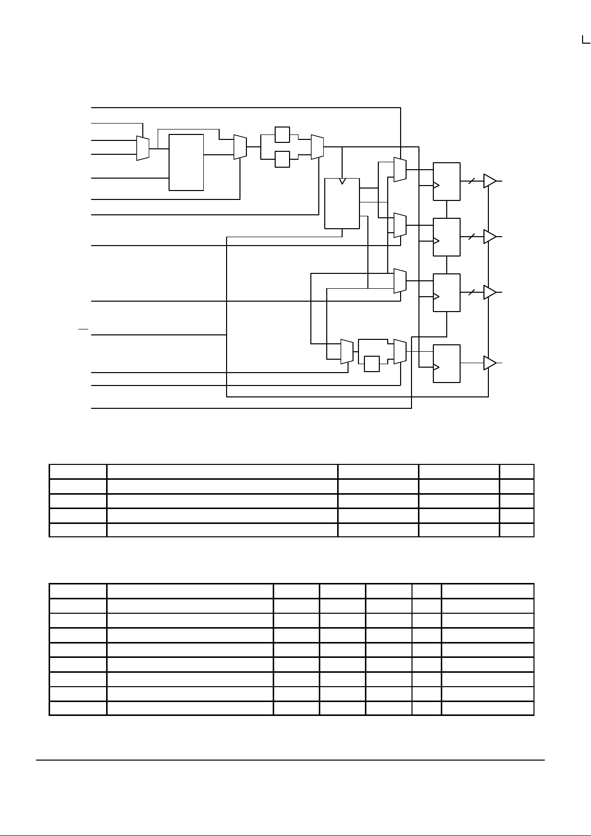
Figure 2. Logic Diagram
PLL
Qa0:4
Q
TCLK0
FB_In
0
1
D
0
1
TCLK1
TCLK_Sel
÷
2
÷
4
0
1
PLL_EN
R
÷
2
÷
4
÷
6
VCO_Sel
R
0
1
5
Qb0:4
Q
D
R
0
1
5
Qc0:3
Q
D
R
0
1
4
QFB
Q
D
R
0
1
0
1
÷
2
fselb
fselc
fsela
MR
OE
fselFB0
fselFB1
(Int. Pulldown)
(Int. Pullup)
(Int. Pullup)
(Int. Pulldown)
(Int. Pullup)
(Int. Pulldown)
(Int. Pulldown)
(Int. Pulldown)
(Int. Pulldown)
(Int. Pullup)
(Int. Pullup)
(Int. Pulldown)
(Int. Pulldown)
ABSOLUTE MAXIMUM RATINGS*
Symbol Parameter Min Max Unit
V
CC
Supply Voltage –0.3 5.6 V
V
I
Input Voltage –0.3 VDD + 0.3 V
I
IN
Input Current 8 mA
T
Stor
Storage Temperature Range –40 125 °C
* Absolute maximum continuous ratings are those values beyond which damage to the device may occur. Exposure to these conditions or conditions beyond those
indicated may adversely affect device reliability. Functional operation under absolute-maximum-rated conditions is not implied.
DC CHARACTERISTICS (TA = 0° to 70°C, VCC = 3.3V ±5%)
Symbol Characteristic Min Typ Max Unit Condition
V
IH
Input HIGH Voltage 2.0 V
CC
V
V
IL
Input LOW Voltage 0.8 V
V
OH
Output HIGH Voltage 2.4 V IOH = –20mA (Note 1.)
V
OL
Output LOW Voltage 0.5 V IOL = 20mA (Note 1.)
I
IN
Input Current ±100 µA Note 2.
I
CC
Maximum Quiescent Supply Current 120 mA
C
IN
Input Capacitance 8 pF
C
pd
Power Dissipation Capacitance 25 pF Per Output
1. The MPC974 outputs can drive series or parallel terminated 50Ω (or 50Ω to VCC/2) transmission lines on the incident edge (see Applications
Info section).
2. Inputs have either pull–up or pull–down resistors which affect input current.
 Loading...