

Motorola MPC973FA, MPC972FA Datasheet

SEMICONDUCTOR TECHNICAL DATA
1
REV 1
Motorola, Inc. 1997
8/97
The MPC972/973 are 3.3V compatible, PLL based clock driver
devices targeted for high performance CISC or RISC processor based
systems. With output frequencies of up to 125MHz and skews of 550ps
the MPC972/973 are ideally suited for most synchronous systems. The
devices offer twelve low skew outputs plus a feedback and sync output for
added flexibility and ease of system implementation.
• Fully Integrated PLL
• Output Frequency up to 125MHz
• Compatible with PowerPC and Pentium Microprocessors
• TQFP Packaging
• 3.3V V
CC
• ± 100ps Typical Cycle–to–Cycle Jitter
The MPC972/973 features an extensive level of frequency
programmability between the 12 outputs as well as the input vs output
relationships. Using the select lines output frequency ratios of 1:1, 2:1,
3:1, 3:2, 4:1, 4:3, 5:1, 5:2, 5:3, 6:1 and 6:5 between outputs can be
realized by pulsing low one clock edge prior to the coincident edges of the
Qa and Qc outputs. The Sync output will indicate when the coincident
rising edges of the above relationships will occur. The selectability of the
feedback frequency is independent of the output frequencies, this allows
for very flexible programming of the input reference vs output frequency
relationship. The output frequencies can be either odd or even multiples
of the input reference. In addition the output frequency can be less than
the input frequency for applications where a frequency needs to be
reduced by a non–binary factor. The Power–On Reset ensures proper
programming if the frequency select pins are set at power up. If the
fselFB2 pin is held high, it may be necessary to apply a reset after
power–up to ensure synchronization between the QFB output and the
other outputs. The internal power–on reset is designed to provide this
function, but with power–up conditions being system dependent, it is
difficult to guarantee. All other conditions of the fsel pins will automatically
synchronize during PLL lock acquisition.
The MPC972/973 offers a very flexible output enable/disable scheme. This enable/disable scheme helps facilitate system
debug as well as provide unique opportunities for system power down schemes to meet the requirements of “green” class
machines. The MPC972 allows for the enabling of each output independently via a serial input port. When disabled or “frozen”
the outputs will be locked in the “LOW” state, however the internal state machines will continue to run. Therefore when “unfrozen”
the outputs will activate synchronous and in phase with those outputs which were not frozen. The freezing and unfreezing of
outputs occurs only when they are already in the “LOW” state, thus the possibility of runt pulse generation is eliminated. A
power-on reset will ensure that upon power up all of the outputs will be active. Note that all of the control inputs on the
MPC972/973 have internal pull–up resistors.
The MPC972/973 is fully 3.3V compatible and requires no external loop filter components. All inputs accept LVCMOS/LVTTL
compatible levels while the outputs provide LVCMOS levels with the capability to drive 50Ω transmission lines. For series
terminated lines each MPC972/973 output can drive two 50Ω lines in parallel thus effectively doubling the fanout of the device.
The MPC972/973 can consume significant power in some configurations. Users are encouraged to review Application Note
AN1545/D in the Timing Solutions book (BR1333/D) for a discussion on the thermal issues with the MPC family of clock drivers.
PowerPC is a trademark of International Business Machines Corporation. Pentium is a trademark of Intel Corporation.
LOW VOLTAGE
PLL CLOCK DRIVER
FA SUFFIX
52–LEAD TQFP PACKAGE
CASE 848D-03

MPC972 MPC973
MOTOROLA TIMING SOLUTIONS
BR1333 — Rev 6
2
fselb1
fselb0
fsela1
fsela0
Qa3
VCCO
Qa2
GNDO
Qa1
VCCO
Qa0
GNDO
VCO_Sel
fselFB1
QSync
GNDO
Qc0
VCCO
Qc1
fselc0
fselc1
Qc2
VCCO
Qc3
GNDO
Inv_Clk
GNDO
Qb0
VCCO
Qb1
GNDO
Qb2
VCCO
Qb3
Ext_FB
GNDO
QFB
VCCI
fselFB0
GNDI
MR/OE
Frz_Clk
Frz_Data
fselFB2
PLL_EN
Ref_Sel
TClk_Sel
TClk0
TClk1
xtal1 (972)
xtal2 (972)
VCCA
40
41
42
43
44
45
46
47
48
49
50
51
52
25
24
23
22
21
20
19
18
17
16
15
14
12345678910111213
39 38 37 36 35 34 33 32 31 30 29 28 27
26
MPC972/
MPC973
PECL_CLK (973)
PECL_CLK (973)
Figure 1. 52–Lead Pinout (Top View)
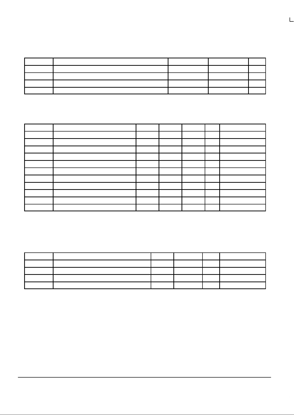
FUNCTION TABLE 1
fsela1 fsela0 Qa fselb1 fselb0 Qb fselc1 fselc0 Qc
0
0
1
1
0
1
0
1
÷4
÷6
÷8
÷12
0
0
1
1
0
1
0
1
÷4
÷6
÷8
÷10
0
0
1
1
0
1
0
1
÷2
÷4
÷6
÷8
FUNCTION TABLE 2
fselFB2 fselFB1 fselFB0 QFB
0
0
0
0
0
0
1
1
0
1
0
1
÷4
÷6
÷8
÷10
1
1
1
1
0
0
1
1
0
1
0
1
÷8
÷12
÷16
÷20
FUNCTION TABLE 3
Control Pin Logic ‘0’ Logic ‘1’
VCO_Sel VCO/2 VCO
Ref_Sel TCLK Xtal (PECL)
TCLK_Sel TCLK0 TCLK1
PLL_En Bypass PLL Enable PLL
MR/OE Master Reset/Output Hi–Z Enable Outputs
Inv_Clk Non–Inverted Qc2, Qc3 Inverted Qc2, Qc3
MPC972 MPC973
TIMING SOLUTIONS
BR1333 — Rev 6
3 MOTOROLA
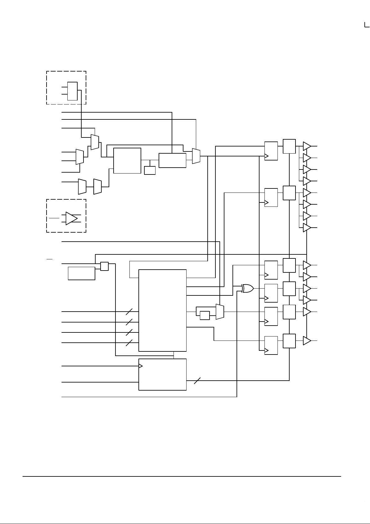
Figure 2. Logic Diagram
POWER-ON
RESET
VCO
PHASE
DETECTOR
LPF
PLL_En
Qa0
VCO_Sel
Q
Qa1
TCLK0
REF_SEL
Ext_FB
0
1
D
Qa2
Qa3
Sync
Frz
Qb0
Q
Qb1
D
Qb2
Qb3
Sync
Frz
Qc0
Q
Qc1
D
Qc2
Qc3
Sync
Frz
QFB
QD
Sync
Frz
fsela0:1
fselb0:1
Frz_Data
fselc0:1
fselFB0:1
÷
4, ÷6, ÷8, ÷12
÷
4, ÷6, ÷8, ÷10
÷
2, ÷4, ÷6, ÷8
0
1
QSync
QD
Sync
Frz
÷
2
÷
4, ÷6, ÷8, ÷10
Sync Pulse
Data Generator
Output Disable
Circuitry
Frz_Clk
12
2
2
2
2
MR/OE
0
1
TCLK1
TCLK_Sel
QD
Sync
Frz
Inv_Clk
fselFB2
xtal2
xtal1
972 OPTION
PCLK
PCLK
973 OPTION

MPC972 MPC973
MOTOROLA TIMING SOLUTIONS
BR1333 — Rev 6
4
Figure 3. Timing Diagrams
fVCO
1:1 Mode
Qa
Qc
Sync
2:1 Mode
Qc(÷2)
Qa(÷6)
Sync
3:1 Mode
Qa
Qc
Sync
Qa(÷4)
Qc(
÷
6)
Sync
3:2 Mode
Qc(÷2)
Qa(
÷
8)
Sync
4:1 Mode
Qa(÷6)
Qc(
÷
8)
Sync
4:3 Mode
Qa(÷12)
Qc(÷2)
Sync
6:1 Mode
MPC972 MPC973
TIMING SOLUTIONS
BR1333 — Rev 6
5 MOTOROLA
ABSOLUTE MAXIMUM RATINGS*
Symbol Parameter Min Max Unit
V
CC
Supply Voltage –0.3 4.6 V
V
I
Input Voltage –0.3 VDD + 0.3 V
I
IN
Input Current ±20 mA
T
Stor
Storage Temperature Range –40 125 °C
* Absolute maximum continuous ratings are those values beyond which damage to the device may occur. Exposure to these conditions or
conditions beyond those indicated may adversely affect device reliability. Functional operation under absolute-maximum-rated conditions is not
implied.
DC CHARACTERISTICS (Note 4.; TA = 10° to 70°C; VCC = 3.3V ±5%)
Symbol Characteristic Min Typ Max Unit Condition
V
IH
Input HIGH Voltage 2.0 3.6 V
V
IL
Input LOW Voltage 0.8 V
V
PP
Peak–to–Peak Input Voltage PECL_CLK 300 1000 mV
V
CMR
Common Mode Range PECL_CLK VCC–2.0 VCC–0.6 Note 1.
V
OH
Output HIGH Voltage 2.4 V IOH = –20mA (Note 2.)
V
OL
Output LOW Voltage 0.5 V IOL = 20mA (Note 2.)
I
IN
Input Current ±120 µA Note 3.
I
CC
Maximum Quiescent Supply Current 190 215 mA All VCC PIns
I
CCA
Analog VCC Current 15 20 mA
C
IN
Input Capacitance 4 pF
C
pd
Power Dissipation Capacitance 25 pF Per Output
1. V
CMR
is the difference from the most positive side of the differential input signal. Normal operation is obtained when the “High” input is within
the V
CMR
range and the input lies within the VPP specification.
2. The MPC972/973 outputs can drive series or parallel terminated 50Ω (or 50Ω to VCC/2) transmission lines on the incident edge (see Applications
Info section).
3. Inputs have pull–up/pull–down resistors which affect input current.
4. Special thermal handling may be required in some configurations.
PLL INPUT REFERENCE CHARACTERISTICS (TA = 10° to 70°C)
Symbol Characteristic Min Max Unit Condition
tr, t
f
TCLK Input Rise/Falls 3.0 ns
f
ref
Reference Input Frequency Note 5. 100, Note 5. MHz Note 5.
f
refDC
Reference Input Duty Cycle 25 75 %
t
xtal
Crystal Oscillator Frequency 10 25 MHz Note 6.
5. Maximum input reference frequency is limited by the VCO lock range and the feedback divider or 100MHz, minimum input reference frequency
is limited by the VCO lock range and the feedback divider.
6. See Applications Info section for more crystal information.
 Loading...