Motorola MPC953FA Datasheet

SEMICONDUCTOR TECHNICAL DATA
1
REV 0.1
Motorola, Inc. 1997
9/97
The MPC953 is a 3.3V compatible, PLL based clock driver device
targeted for high performance clock tree designs. With output frequencies
of up to 87.5MHz and output skews of 150ps the MPC953 is ideal for the
most demanding clock tree designs. The devices employ a fully
differential PLL design to minimize cycle–to–cycle and phase jitter.
• Fully Integrated PLL
• Output Frequency up to 87.5MHz
• Outputs Disable in High Impedance
• TQFP Packaging
• 100ps Cycle–to–Cycle Jitter
The MPC953 has a differential LVPECL reference input along with an
external feedback input. These features make the MPC953 ideal for use
as a zero delay, low skew fanout buffer. The device performance has
been tuned and optimized for zero delay performance. The MR/OE
input
pin will reset the internal counters and tristate the output buffers when
driven “high”.
If the reference clock (PECL_CLK) is lost or shut down when the
MPC953 is in phase–lock, the output frquency will slew slowly downward.
The final VCO frequency will be around TBDMHz.
The MPC953 is fully 3.3V compatible and requires no external loop
filter components. All control inputs accept LVCMOS or LVTTL
compatible levels while the outputs provide LVCMOS levels with the
ability to drive terminated 50Ω transmission lines. For series terminated
50Ω lines, each of the MPC953 outputs can drive two traces giving the
device an effective fanout of 1:18. The device is packaged in a 7x7mm
32–lead TQFP package to provide the optimum combination of board
density and performance.
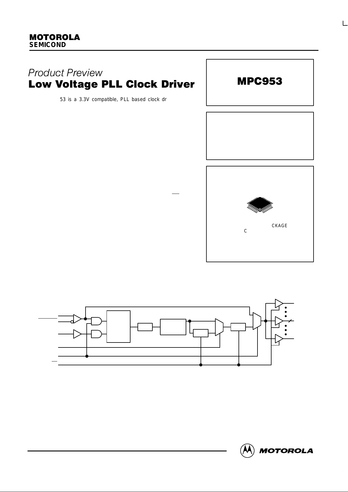
Figure 1. Logic Diagram
PECL_CLK
PECL_CLK
FB_CLK
Phase
Detector
LPF
VCO
200–350MHz
÷
4
VCO_SEL
BYPASS
QFB
Q0:6
Q7
7
÷
2
MR/OE
This document contains information on a product under development. Motorola reserves the right to change or
discontinue this product without notice.
LOW VOLTAGE
PLL CLOCK DRIVER
FA SUFFIX
32–LEAD TQFP PACKAGE
CASE 873A–02

MPC953
MOTOROLA ECLinPS and ECLinPS Lite
DL140 — Rev 3
2
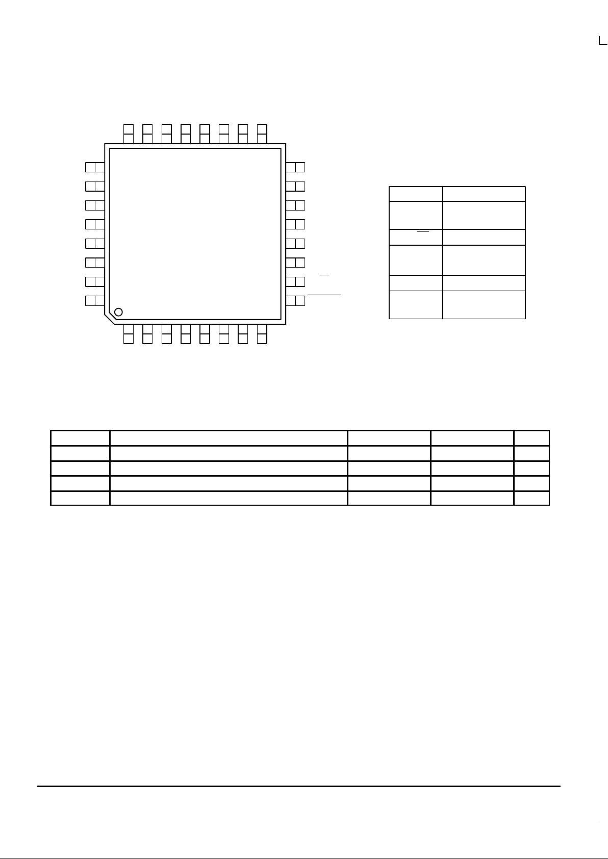
MR/OE
GNDO
Q0
VCCO
QFB
GNDO
NC
BYPASS
VCO_SEL
Q5
VCCO
Q6
GNDO
Q7
VCCO
Q1
VCCOQ2GNDOQ3VCCOQ4GNDO
VCCA
FB_CLK
NC
NC
NC
NC
GNDI
PECL_CLK
25
26
27
28
29
30
31
32
15
14
13
12
11
10
9
12345678
24 23 22 21 20 19 18 17
16
MPC953
FUNCTION TABLES
BYPASS Function
1
0
PLL Enabled
PLL Bypass
MR/OE Function
1
0
Outputs Disabled
Outputs Enabled
Figure 2. 32–Lead Pinout (Top View)
PECL_CLK
VCO_SEL Function
1
0
÷2
÷1
ABSOLUTE MAXIMUM RATINGS*
Symbol Parameter Min Max Unit
V
CC
Supply Voltage –0.3 4.6 V
V
I
Input Voltage –0.3 VDD + 0.3 V
I
IN
Input Current ±20 mA
T
Stor
Storage Temperature Range –40 125 °C
* Absolute maximum continuous ratings are those values beyond which damage to the device may occur. Exposure to these conditions or
conditions beyond those indicated may adversely affect device reliability. Functional operation under absolute–maximum–rated conditions is
not implied.

MPC953
ECLinPS and ECLinPS Lite
DL140 — Rev 3
3 MOTOROLA
DC CHARACTERISTICS (TA = 0° to 70°C, VCC = 3.3V ±5%)
Symbol Characteristic Min Typ Max Unit Condition
V
IH
Input HIGH Voltage LVCMOS Inputs 2.0 3.6 V
V
IL
Input LOW Voltage LVCMOS Inputs 0.8 V
V
PP
Peak–to–Peak Input Voltage PECL_CLK 300 1000 mV
V
CMR
Common Mode Range PECL_CLK VCC–1.5 VCC–0.6 mV Note 1.
V
OH
Output HIGH Voltage 2.4 V IOH = –40mA, Note 2.
V
OL
Output LOW Voltage 0.5 V IOL = 40mA, Note 2.
I
IN
Input Current ±120 µA
C
IN
Input Capacitance 4 pF
C
pd
Power Dissipation Capacitance 25 pF Per Output
I
CC
Maximum Quiescent Supply Current 75 mA All VCC Pins
I
CCPLL
Maximum PLL Supply Current 15 20 mA VCCA Pin Only
1. V
CMR
is the difference from the most positive side of the differential input signal. Normal operation is obtained when the “HIGH” input is within
the V
CMR
range and the input swing lies within the VPP specification.
2. The MPC953 outputs can drive series or parallel terminated 50Ω (or 50Ω to VCC/2) transmission lines on the incident edge (see Applications
Info section).
PLL INPUT REFERENCE CHARACTERISTICS (TA = 0 to 70°C)
Symbol Characteristic Min Max Unit Condition
f
ref
Reference Input Frequency Note 3. Note 3. MHz
f
refDC
Reference Input Duty Cycle 25 75 %
3. Maximum and minimum input reference is limited by the VCO lock range and the feedback divider.
AC CHARACTERISTICS (TA = 0°C to 70°C, VCC = 3.3V ±5%)
Symbol Characteristic Min Typ Max Unit Condition
tr, t
f
Output Rise/Fall Time 0.10 1.0 ns 0.8 to 2.0V
t
pw
Output Duty Cycle 45 50 55 %
t
sk(O)
Output–to–Output Skews (Relative to QFB) ±75 ps
f
VCO
PLL VCO Lock Range 200 350 MHz
f
max
Maximum Output Frequency 50 87.5 MHz VCO_SEL = ‘0’
tpd(lock) Input to Ext_FB Delay (with PLL Locked) X–100 X
(Note 4.)
X+100 ps f
ref
= 75MHz
tpd(bypass) Input to Q Delay (with PLL Bypassed) 5 10 ns
t
PLZ,HZ
Output Disable Time 7 ns
t
PZL
Output Enable Time 6 ns
t
jitter
Cycle–to–Cycle Jitter (Peak–to–Peak) 100 ps
t
lock
Maximum PLL Lock Time 10 ms
4. X will be targeted for 0ns, but may vary from target by ±150ps based on characterization of silicon.
 Loading...