

Motorola MPC949FA Datasheet
SEMICONDUCTOR TECHNICAL DATA
1
REV 1
Motorola, Inc. 1996
10/96
The MPC949 is a low voltage CMOS, 15 output clock buffer. The 15
outputs can be configured into a standard fanout buffer or into 1X and
1/2X combinations. The device features a low voltage PECL input, in
addition to its LVCMOS/LVTTL inputs, to allow it to be incorporated into
larger clock trees which utilize low skew PECL devices (see the
MC100LVE111 data sheet) in the lower branches of the tree. The fifteen
outputs were designed and optimized to drive 50Ω series or parallel
terminated transmission lines. With output to output skews of 300ps the
MPC949 is an ideal clock distribution chip for synchronous systems
which need a tight level of skew from a large number of outputs. For a
similar product with a smaller fanout and package consult the MPC946
data sheet.
• Clock Distribution for Pentium Systems with PCI
• Low Voltage PECL Clock Input
• 2 Selectable LVCMOS/LVTTL Clock Inputs
• 350ps Maximum Output to Output Skew
• Drives up to 30 Independent Clock Lines
• Maximum Output Frequency of 150MHz
• High Impedance Output Enable
• 52–Lead TQFP Packaging
• 3.3V V
CC
Supply
With an output impedance of approximately 7Ω, in both the HIGH and
the LOW logic states, the output buffers of the MPC949 are ideal for
driving series terminated transmission lines. More specifically each of the
15 MPC949 outputs can drive two series terminated transmission lines.
With this capability, the MPC949 has an effective fanout of 1:30 in
applications using point–to–point distribution schemes.
The MPC949 has the capability of generating 1X and 1/2X signals from a 1X source. The design is fully static, the signals are
generated and retimed inside the chip to ensure minimal skew between the 1X and 1/2X signals. The device features selectability
to allow the user to select the ratio of 1X outputs to 1/2X outputs.
Two independent LVCMOS/LVTTL compatible clock inputs are available. Designers can take advantage of this feature to
provide redundant clock sources or the addition of a test clock into the system design. With the TCLK_Sel input pulled HIGH the
TCLK1 input is selected. The PCLK_Sel input will select the PECL input clock when driven HIGH.
All of the control inputs are LVCMOS/LVTTL compatible. The Dsel pins choose between 1X and 1/2X outputs. A LOW on the
Dsel pins will select the 1X output. The MR/OE
input will reset the internal flip flops and tristate the outputs when it is forced HIGH.
The MPC949 is fully 3.3V compatible. The 52 lead TQFP package was chosen to optimize performance, board space and cost
of the device. The 52–lead TQFP has a 10x10mm body size with a 0.65mm pin spacing.
Pentium is a trademark of Intel Corporation.
LOW VOLTAGE
1:15 PECL TO CMOS
CLOCK DRIVER
FA SUFFIX
52–LEAD TQFP PACKAGE
CASE 848D–03
MPC949
MOTOROLA TIMING SOLUTIONS
BR1333 — Rev 6
2
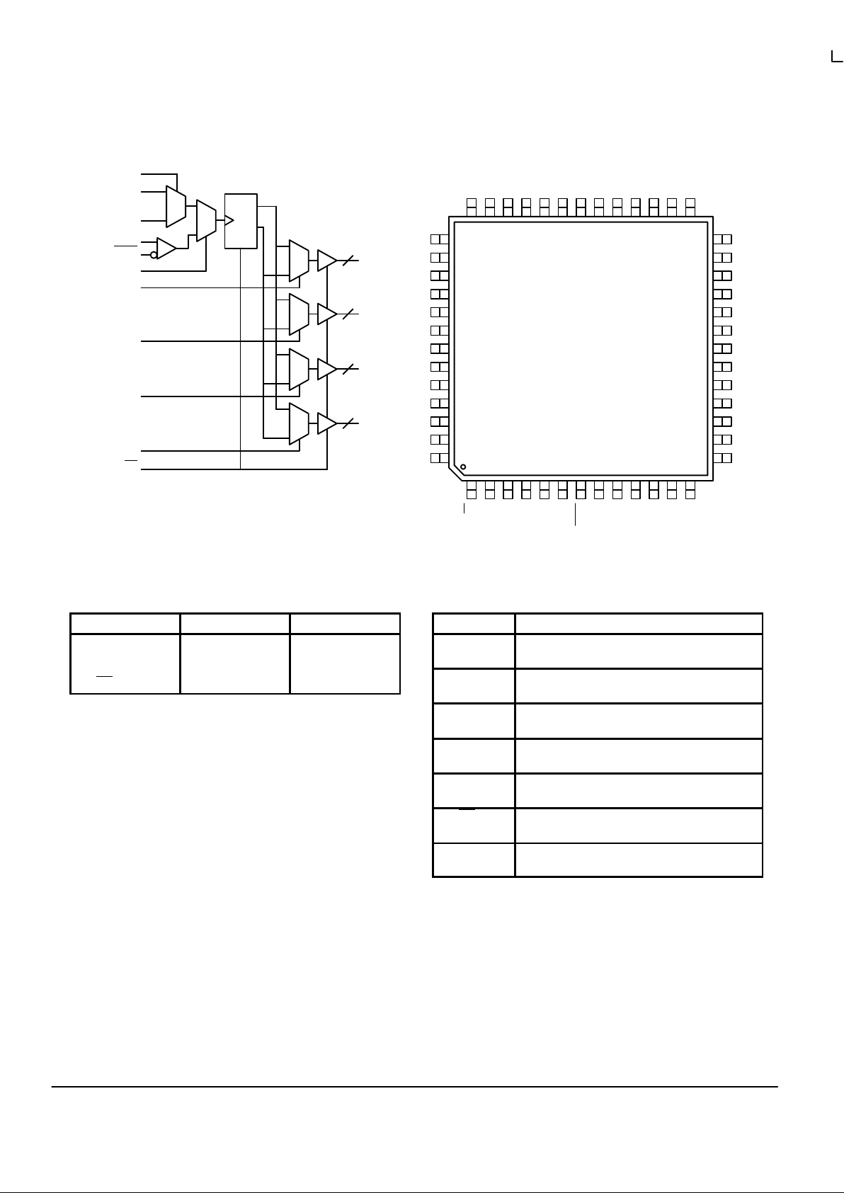
Figure 1. Logic Diagram Figure 2. 52–Lead Pinout (Top View)
NC
VCCb
Qb2
GNDb
Qb1
VCCb
Qb0
GNDb
GNDa
Qa1
VCCa
Qa0
GNDa
NC
VCCd
Qd4
GNDd
Qd3
VCCd
Qd2
GNDd
Qd1
VCCd
Qd0
GNDd
NC
NC
GNDc
Qc0
VCCc
Qc1
GNDc
Qc2
VCCc
Qc3
GNDc
GNDd
Qd5
NC
TCLK_Sel
MR/OE
VCCI
TCLK0
TCLK1
PCLK
PCLK
PCLK_Sel
Dsela
Dselb
Dselc
Dseld
GNDI
40
41
42
43
44
45
46
47
48
49
50
51
52
25
24
23
22
21
20
19
18
17
16
15
14
12345678910111213
39 38 37 36 35 34 33 32 31 30 29 28 27
26
MPC949
TCLK1 (LVTTL)
Qa0:1
TCLK0 (LVTTL)
TCLK_Sel
2
R
÷
2
÷
1
Dsela
Qc0:3
4
Dselc
Qd0:5
6
Dseld
MR/OE
Qb0:2
3
Dselb
PCLK
PCLK
PCLK_Sel
0
1
0
1
0
1
0
1
0
1
0
1
FUNCTION TABLE
Input 0 1
TCLK_Sel
PCLK_Sel
Dseln
MR/OE
TCLK0
TCLKn
÷1
Enabled
TCLK1
PCLK
÷2
Hi–Z
PIN DESCRIPTION
Pin Name Function
TCLK_Sel
(Int Pulldown)
Select pin to choose TCKL0 or TCLK1
TCLK0:1
(Int Pullup)
LVCMOS/LVTTL clock inputs
PCLK
(Int Pulldown)
True PECL clock input
PCLK
(Int Pullup)
Compliment PECL clock input
Dseln
(Int Pulldown)
1x or 1/2x input divide select pins
MR/OE
(Int Pulldown)
Internal reset and output tristate control pin
PCLK_Sel
(Int Pulldown)
Select Pin to choose TCLK or PCLK
 Loading...