

Page 1

查询MPC561MZP40供应商
MOTOROLA
Rev. 1, December 2001
MPC561PB/D
SEMICONDUCTOR
PRODUCT BRIEF
MPC561/MPC562
MPC563/MPC564
Product Brief
MPC561/MPC562 / MPC563/MPC564 RISC MCU
Including Peripheral Pin Multiplexing with
Flash and Code Compression Options
Features
The MPC561/MPC562 / MPC563/MPC564 are members of the Motorola MPC500 RISC Microcontroller
family. As shown in the block diagram, they are composed of:
• High performance CPU system
— High performance core
• Single issue integer core
• Compatible with PowerPC instruction set architecture
• Precise exception model
• Floating point
• Extensive system development support
— On-chip watchpoints and breakpoints
— Program flow tracking
— Background debug mode (BDM)
— IEEE-ISTO Nexus 5001-1999 Class 3 Debug Interface
— MPC500 system interface (USIU, BBC, L2U)
— Fully static design
— Four major power saving modes
• On, doze, sleep, deep-sleep and power-down
— 32-Kbyte static RAM (CALRAM)
— 512-Kbyte flash (UC3F) on MPC563/MPC564
— General-purpose I/O support
• On address (24) and data (32) pins
• 16 GPIO in MIOS14
• Many peripheral pins can be used as GPIO when not used as primary functions
• 2.6-V outputs on external bus pins
• PPM (peripheral pin multiplexing with parallel-to-serial driver) module
• Available in package or die
— Plastic ball grid array (PBGA) packaging
Key Feature Details
MPC500 System Interface (USIU)
• System configuration and protection features:
— Periodic-interrupt timer
— Bus monitor
— Software watchdog timer
— Real-time clock (RTC)
This document contains information on a new product. Specifications and
information herein are subject to change without notice.
© MOTOROLA 2001, All Rights Reserved
Page 2

— Decrementer
— Time base
• Clock synthesizer
• Power management
• Reset controller
• External bus interface that tolerates 5-V inputs, provides 2.6-V outputs and supports multiple-mas-
ter designs
• Enhanced interrupt controller that supports up to eight external and 40 internal interrupts, simpli-
fies the interrupt structure and decreases interrupt processing time
• USIU supports dual mapping to map part of one internal/external memory to another external
memory
• USIU supports dual mapping of flash on MPC563 and MPC564 to move part of internal flash mem-
ory to external bus for development
• External bus, supporting non-wraparound burst for instruction fetches, with up to 8 instructions per
memory cycle
Burst Buffer Controller (BBC) Module
• Support for enhanced interrupt controller (EIC)
• Support for enhanced exception table relocation feature
• Branch target buffer
• Contains 2-Kbytes of decompression RAM (DECRAM) for code compression. This RAM may also
be used as general-purpose RAM when code compression feature not used.
Flexible Memory Protection Unit
• Flexible memory protection units (MPU) in BBC and L2U
• Default attributes available in one global entry
• Attribute support for speculative accesses
• Up to eight memory regions are supported, four for data and four for instructions
Memory Controller
• Four flexible chip selects via memory controller
• 24-bit address and 32-bit data buses
• 4-Kbyte to one 16-Mbyte (data) or four-Gbyte (instruction) region size support
• Supports enhanced external burst
• Up to eight-beat transfer bursts, two-clock minimum bus transactions
• Use with SRAM, EPROM, flash and other peripherals
• Byte selects or write enables
• 32-bit address decodes with bit masks
• Four regions
512-Kbytes of CDR3 Flash EEPROM Memory (UC3F) – MPC563 Only
• One 512-Kbyte module
• Page read mode
• Block (64 Kbytes) erasable
• External 4.75- to 5.25-V VFLASH power supply for program, erase, and read operations
32-Kbyte static RAM (CALRAM)
• Composed of one 32-Kbyte CALRAM module
— 28-Kbyte static RAM
— 4-Kbyte calibration (overlay) RAM feature that allows calibration of flash-based constants
• Eight 512-byte overlay regions
• One clock fast accesses
• Two-clock cycle access option for power saving
• Keep-alive power (VDDSRAM) for data retention
MPC561/MPC563 PRODUCT BRIEF MOTOROLA
2
Page 3

General-Purpose I/O Support
• 24 Address pins and 32 data pins can be used for general-purpose I/O in single-chip mode
• 16 GPIO in MIOS14
• Many peripheral pins can be used as GPIO when not used as primary functions
• 2.6-V outputs on external bus pins
• 5-V outputs with slew rate control
NEXUS Debug Port (Class 3)
• Compliant with Class 3 of the IEEE-ISTO Nexus 5001-1999
• Program trace via branch trace messaging (BTM)
• Data trace via data write messaging (DWM) and data read messaging (DRM)
• Ownership trace via ownership trace messaging (OTM)
• Run-time access to on-chip memory map and MPC5xx special purpose registers (SPRs) via the
READI read/write access protocol
• Watchpoint messaging via the auxiliary port
• Reduced-port mode (1 MDI, 2 MDO) or full-port mode (2 MDI. 8 MDO)
• All features configurable and controllable via the auxiliary port
• Security features for production environment
• Supports the RCPU debug mode via the auxiliary port
• READI module can be reset independent of system reset
Integrated I/O System
Two Time Processor Units (TPU3)
• True 5-V I/O
• Two time processing units (TPU3) with16 channels each
• Each TPU3 is a micro-coded timer subsystem
• Eight-Kbytes of dual port TPU RAM (DPTRAM) shared by two TPU3 modules for TPU micro-code
22-Channel Modular I/O System (MIOS14)
• Six modulus counter sub-modules (MCSM)
• 10 double-action sub-modules (DASM)
• 12 dedicated PWM sub-modules (PWMSM)
• One MIOS14 16-bit parallel port I/O sub-modules (MPIOSM)
Two Enhanced Queued Analog-to-Digital Converter Modules (QADC64E)
• Two queued analog-to-digital converter modules (QADC64_A, QADC64_B) providing a total of 32
analog channels
• 16 analog input channels on each QADC64E module using internal multiplexing
• Directly supports up to four external multiplexers
• Up to 41 total input channels on the two QADC64E modules with external multiplexing
• Software configurable to operate in Enhanced or Legacy (MPC555 compatible) mode
• Unused analog channels can be used as digital input/output pins
— GPIO on all channels in Enhanced mode
• 10-bit A/D converter with internal sample/hold
• Typical conversion time of less than 5 µs (>200 K samples/second)
• Two conversion command queues of variable length
• Automated queue modes initiated by:
— External edge trigger
— Software command
— Periodic/interval timer within QADC64E module, that can be assigned to both queue 1 and 2
— External Gated trigger (queue 1only)
• 64 result registers
— Output data is right- or left-justified, signed or unsigned
MPC561/MPC563 PRODUCT BRIEF MOTOROLA
3
Page 4

• Alternate reference input (ALTREF), with control in the conversion command word (CCW)
Three CAN 2.0B Controller (TouCAN) Modules
• Three TouCAN modules (TOUCAN_A, TOUCAN_B, TOUCAN_C)
• Each TouCAN provides the following features:
— 16 message buffers each, programmable I/O modes
— Maskable interrupts
— Independent of the transmission medium (external transceiver is assumed)
— Open network architecture, multi-master concept
— High immunity to EMI
— Short latency time for high-priority messages
— Low-power sleep mode, with programmable wake-up on bus activity
— TOUCAN_C pins are shared with MIOS14 GPIO or QSMCM
Queued Serial Multi-Channel Module (QSMCM)
• One queued serial module with one queued SPI and two SCIs (QSMCM)
• QSMCM matches full MPC555 QSMCM functionality
• Queued SPI
— Provides full-duplex communication port for peripheral expansion or inter-processor commu-
nication
— Up to 32 preprogrammed transfers, reducing overhead
— Synchronous serial interface with baud rate of up to system clock / 4
— Four programmable peripheral-selects pins:
— Support up to 16 devices with external decoding
— Support up to eight devices with internal decoding
— Special wrap-around mode allows continuous sampling of a serial peripheral for efficient inter-
facing to serial analog-to-digital (A/D) converters
• SCI
— UART mode provides NRZ format and half- or full-duplex interface
— 16 register receive buffers and 16 register transmit buffers on one SCI
— Advanced error detection and optional parity generation and detection
— Word-length programmable as eight or nine bits
— Separate transmitter and receiver enable bits, and double buffering of data
— Wake-up functions allow the CPU to run uninterrupted until either a true idle line is detected,
or a new address byte is received
Peripheral Pin Multiplexing (PPM) PPM
• Synchronous serial interface between the microprocessor and an external device
• Four internal parallel data sources can be multiplexed through the PPM
— TPU3_A: 16 channels
— TPU3_B: 16 channels
— MIOS14: 12 PWM channels, 4 MDA channels
— Internal GPIO: 16 general-purpose inputs, 16 general-purpose outputs
• Software configurable stream size
• Software configurable clock (TCLK) based on system clock
• Software selectable clock modes (SPI mode and TDM mode)
• Software selectable operation modes
— Continuous mode
— Start-transmit-receive (STR) mode
• Software configurable internal modules interconnect (shorting)
MPC561/MPC563 PRODUCT BRIEF MOTOROLA
4
Page 5

MPC561/MPC562 / MPC563/MPC564 Optional Features
The following are optional features of the MPC561/MPC562 / MPC563/MPC564:
• 56-MHz operation (40 MHz is default)
• Code compression supported on the MPC562 and the MPC564
— Compression reduces instruction memory requirements by 40-50%
— Compression optimized for automotive (non-cached) applications
• 512 Kbytes flash (available on the MPC563/MPC564 only)
— Single array
— Page mode read
— Block (64 Kbytes) erasable
— External 4.75- to 5.25-V VFLASH program, erase, and read power supply
512 Kbytes
JTAG
Burst
Buffer
Controller
MPC5xx
Core
+
FP
Flash
(on MPC563/
MPC564 only)
U-BUS
USIU
READI
E-BUS
QADC64
TPU3
L-BUS
32-Kbyte CALRAM
28-Kbyte
SRAM
(No Overlay)
4-Kbyte Overlay
QADC64
8-Kbyte
DPTRAM
QSMCM
TPU3
Tou
CAN
L2U
Int.
PPM
CAN
Tou
UIMB
Tou
CAN
I/F
IMB3
MIOS14
Figure 1 MPC561/MPC562 / MPC563/MPC564 Block Diagram
MPC561/MPC563 PRODUCT BRIEF MOTOROLA
5
Page 6
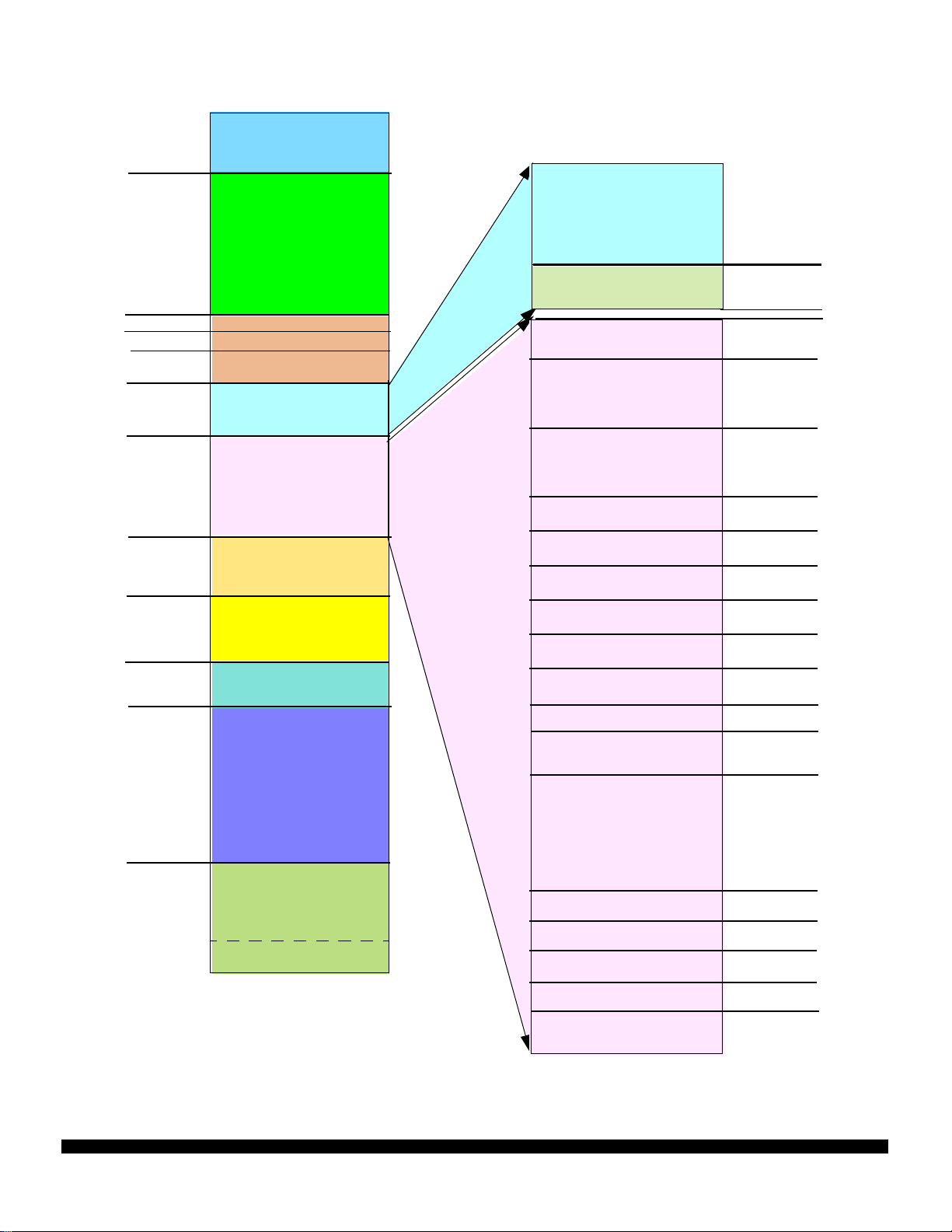
0x00 0000
0x07 FFFF
0x08 0000
0x2F 7FFF
0x2F 8000
0x2F 8800
0x2F A000
0x2F BFFF
0x2F C000
0x2F FFFF
0x30 0000
0x30 7FFF
0x30 8000
0x37 FFFF
0x38 0000
0x38 00FF
0x38 0100
0x38 3FFF
0x38 4000
UC3F Flash*
512 Kbytes
Reserved for Flash
2,605 Kbytes
BBC DECRAM 2 Kbytes
Reserved for BBC
BBC CONTROL
USIU & Flash Control
16 Kbytes
UIMB I/F & IMB
Modules
32 Kbytes
Reserved for IMB
491 Kbytes
CALRAM/
READI Control
256 bytes
Reserved (L-bus Control)
~32 Kbytes
Reserved (L-bus Mem)
464 Kbytes
USIU Control Registers
UC3F Control
Registers*
DPTRAM Control (32 bytes)
Reserved (8160 bytes)
DPTRAM (8 Kbytes)
TPU3_A (1 Kbyte)
TPU3_B (1 Kbyte)
QADC64_A (1 Kbyte)
QADC64_B (1 Kbyte)
QSMCM (1 Kbyte)
Reserved (2 Kbytes)
PPM (64 bytes)
Reserved (960 bytes)
MIOS14 (4 Kbytes)
0x2F C000
0x2F C800
0x30 0000
0x30 0020
0x30 2000
0x30 4000
0x30 4400
0x30 4800
0x30 4C00
0x30 5000
0x30 5400
0x30 5C00
0x30 5C80
0x30 6000
0x3F 7FFF
0x3F 8000
CALRAM
0x3F F000
0x3F FFFF
*NOTE: Only available on MPC563/MPC564.
4-Kbyte Overlay Section
32 Kbytes
TOUCAN_A (1 Kbyte)
TOUCAN_B (1 Kbyte)
TOUCAN_C (1 Kbyte)
Reserved (896 bytes)
UIMB Registers
(128 bytes)
0x30 7000
0x30 7400
0x30 7800
0x30 7C00
0x30 7F80
0x30 7FFF
Figure 2 MPC561 / MPC563 Internal Memory Map
MPC561/MPC563 PRODUCT BRIEF MOTOROLA
6
Page 7
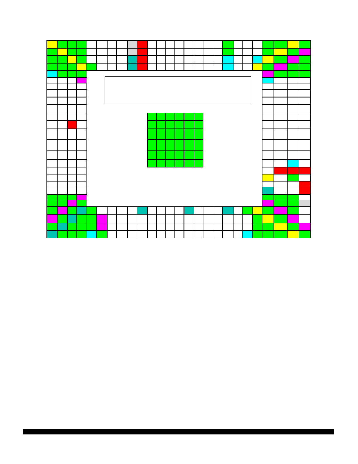
1 2 3 4 5 6 7 8 9 10 11121314 15 1617 18 19 2021 22 23 24 25 26
A VDD VSS VSS VSS
B VSS VDD VSS VSS A_TPUCH2 A_TPUCH6
C VSS VSS VDD VSS
D VSS VSS VSS VDD VSS
E VDDH VSS VSS VSS
B_T2CLK_P
A_T2CLK_
F
CS4
G B_TPUCH12
H
B_TPUCH8 B_TPUCH9
J
B_TPUCH4 B_TPUCH5
K
B_TPUCH0 B_TPUCH1
JCOMP_RS
L
TI_B
TDI_DSDI_
M
MDI0
IRQ3_B_KR
_B_RETRY
N
_B_SGPIO
C3
IRQ4_B_AT
P
2_SGPIOC4
SGPIOC7_I
R
RQOUT_B_
LWP0
T
WE_B_AT0 WE_B_AT1
U
CS0_B CS1_B CS2_B CS3_B
V
RD_WR_B OE_B TEA_B TSIZ0
W TSIZ1 TS_B TA_B BDIP_B HRESET_B SRESET_B
Y
BURST_B
AA VSS VSS VSS QVDDL VSS VSS VSS XFC AA
AB VSS VSS QVDDL VSS QVDDL VSS VSS VSSSYN AB
AC VSS QVDDL VSS NVDDL VSS
AD QVDDL VSS NVDDL VSS VSS QVDDL
AE VSS NVDDL VSS VSS VSS QVDDL
AF NVDDL VSS VSS VSS VDDH VSS
A_TPUCH
PCS5
0
B_TPUCH13B_TPUCH14B_TPUCH1
B_TPUCH10B_TPUCH1
B_TPUCH
6
B_TPUCH
2
TCK_DSCK
B_CNRX0 B_CNTX0
_MCKI
TMS_EVTI_BVDDSRAMTDO_DSD
IWP0_VFLS0IWP1_VFL
S1
IRQ2_B_C
IRQ0_B_S
R_B_SGPI
GPIOC0_
OC2_MDO
MDO4
5_MTS
BB_B_VF2
BG_B_VF
_IWP3
0_LWP1
WE_B_AT2WE_B_AT
BI_B_STS_BADDR_SG
PIOA12
1 2 3 4 5 6 7 8 9 10 11121314 15 16 17 18 19 2021 22 23 24 25 26
A_TPUCH3 A_TPUCH7
A_TPUCH1 A_TPUCH4
QVDDL VDDH
5
1
B_TPUCH7
B_TPUCH3
O_MDO0
SGPIOC6_
FRZ_PTR_
B
IRQ1_B_R
SV_B_SG
PIOC1
BR_B_VF1
_IWP2
3
ADDR_SG
PIOA11
A_TPUCH5
ADDR_SGP
IOA10
A_TPUCH
11 A_TPUCH15
A_TPUCH
A_TPUCH14 VSSA ALTREF
10
A_TPUCH
A_TPUCH12
8
A_TPUCH
A_TPUCH13
9
VSSA VRL
NVDDL VRH
NVDDL VDDA
A_AN3_A
A_AN51_P
NZ_PQB3
QB7
A_AN2_A
A_AN50_P
NY_PQB2
QB6
A_AN0_A
NW_PQB0A_AN48_P
QB4
A_AN1_A
A_AN49_P
NX_PQB1
QB5
A_AN55_
A_AN56_P
PQA3
QA4
A_AN54_
MA2_PQA2A_AN58_P
QA6
A_AN52_
MA0_PQA0A_AN59_P
QA7
A_AN53_
MA1_PQA1A_AN57_P
QA5
B_AN0_AN
W_PQB0
B_AN1_AN
X_PQB1
B_AN2_AN
Y_PQB2
B_AN3_AN
Z_PQB3
B_AN48_
PQB4
B_AN49_
PQB5
B_AN50_
PQB6
B_AN51_
PQB7
B_AN52_M
A0_PQA0
B_AN53_M
A1_PQA1
B_AN54_M
A2_PQA2
B_AN55_P
QA3
B_AN56_P
QA4
B_AN57_P
QA5
B_AN58_P
QA6
B_AN59_P
QA7
MPC561 / MPC563 Ball Map
(As viewed from top, through the package and silicon)
VSS VSS VSS VSS VSS VSS
VSS VSS VSS VSS VSS VSS A_CNTX0
VSS VSS VSS VSS VSS VSS
VSS VSS VSS VSS VSS VSS
VSS VSS VSS VSS VSS VSS
VSS VSS VSS VSS VSS VSS
ADDR_SG
ADDR_SGPI
PIOA18
ADDR_SG
PIOA13
ADDR_SG
PIOA14
ADDR_SG
PIOA15
OA20
ADDR_SGPI
OA16
ADDR_SGPI
OA17
ADDR_SGPI
OA9
ADDR_SG
PIOA23
ADDR_SG
PIOA19
ADDR_SG
PIOA31
ADDR_SG
PIOA8
NVDDL
ADDR_SGP
IOA21
ADDR_SGP
IOA30
ADDR_SGP
IOA22
ADDR_S
GPIOA26
ADDR_S
GPIOA24
ADDR_S
GPIOA28
ADDR_S
GPIOA27
DATA_SG
PIOD1
ADDR_SG
PIOA25
ADDR_SG
PIOA29
DATA_SG
PIOD31
DATA_SG
PIOD5
DATA_SG
PIOD0
DATA_SG
PIOD30
DATA_SG
PIOD3
DATA_SG
PIOD7
DATA_SG
PIOD28
DATA_SG
PIOD29
DATA_SG
PIOD2
NVDDL
DATA_SGP
IOD26
DATA_SGP
IOD27
DATA_SGP
IOD4
DATA_SG
PIOD9
DATA_SG
PIOD24
DATA_SG
PIOD25
DATA_SG
PIOD6
DATA_SGP
IOD11
DATA_SGP
IOD22
DATA_SGP
IOD23
DATA_SGP
IOD8
DATA_SG
PIOD12
DATA_SG
PIOD13
DATA_SG
PIOD21
DATA_SG
PIOD10
VSS
VSS
VDDH
VDDH
NVDDL
DATA_SGPI
OD15
DATA_SGPI
OD19
DATA_SGPI
OD20
ETRIG2_
PCS7 MDA13 MDA28
ETRIG1_
MDA14 MDA29 VSS VDD VSS QVDDL B
PCS6
MDA11 M DA15
MDA12 M DA27
DATA_S
VSS VDD VSS QVDDL VSS EXTAL AC
GPIOD14
IRQ5_B_S
DATA_S
GPIOC5_M
GPIOD16
ODCK1
DATA_S
IRQ6_B_M
GPIOD17
ODCK2
DATA_S
VDDH VSS VSS VSS VDD VSS AF
GPIOD18
VSS VSS VDD VSS A
VDDH VDD VSS QVDDL VSS C
VDD VSS QVDDL VSS VSS D
QVDDL VSS VSS VSS E
MDA30 MDA31
MPWM1_MD
MPWM16
O2
MPWM17_M
MPWM18_MDO6MPWM19_M
DO3
MPIO32B6_
MPIO32B7_MP
MPWM4_MD
WM5
O6
MPIO32B12_
MPIO32B11_C
C_CNTX0
_CNRX0
VF0_MPIO32
VF1_MPIO32B
B0_MDO1
1_MCKO
VFLS0_MPIO
VF2_MPIO32B
32B3_MSEO
2_MSEI_B
PCS2_QGPI
O2
SCK_QGPIO
6
RXD1_QGPI1TXD2_QGPO2
EPEE BOEPEE
CLKOUT VSSF VDDF VFLASH U
VDD EXTCLK VSS
NVDDL
VSS VDD VSS QVDDL XTAL AD
VSS VSS VDD VSS QVDDL AE
_B
PCS0_SS_B_
PCS1_QGPIO1
MOSI_QGPIO5
TXD1_QGPO
_C_CNTX0
PORESET_B
IRQ7_B_MODCK3RSTCONF_B
MPWM0_MD
I1
MPWM3_PP
MPWM2_PP
M_RX1
M_TX1
MPIO32B5_
DO7
MDO5
MPIO32B8_
MPIO32B9_
MPWM20
MPWM21
MPIO32B10_
MPIO32B13_
PPM_TSYNC
PPM_TCLK
MPIO32B15_
MPIO32B14_
PPM_TX0
PPM_RX0
VFLS1_MPIO
32B4
A_CNRX0
QGPIO0
MISO_QGPIO4PCS3_QGPI
O3
PULL-SEL
1
RXD2_QGPI
VDDH
2_C_CNRX0
ENGCLK_BU
CLK
KAPWR W
_TRST_B
VDDSYN Y
_TEXP
NOTE: The flash balls are only available on the MPC563 and MPC564. These are no connect balls on
the MPC561 and MPC562. Flash supplies and inputs are located on the following balls: T23, T24, U24,
U25. U26.
F
G
H
J
K
L
M
N
P
R
T
V
Figure 3 MPC561 / MPC563 Ball Map
MPC561/MPC563 PRODUCT BRIEF MOTOROLA
7
Page 8

Ordering Information
Table 1 MPC561/562 / MPC563/564
Device
Name
MPC561 MPC561MZP40 388 PBGA -40 – 125° C 40 MHz No
MPC561 MPC561CZP40 388 PBGA -40 – 85° C 40 MHz No
MPC561 MPC561MZP56 388 PBGA -40 – 125° C 56 MHz No
MPC561 MPC561CZP56 388 PBGA -40 – 85° C 56 MHz No
MPC562 MPC562MZP40 388 PBGA -40 – 125° C 40 MHz Yes
MPC562 MPC562CZP40 388 PBGA -40 – 85° C 40 MHz Yes
MPC562 MPC562MZP56 388 PBGA -40 – 125° C 56 MHz Yes
MPC562 MPC562CZP56 388 PBGA -40 – 85° C 56 MHz Yes
MPC563 MPC563MZP40 388 PBGA -40 – 125° C 40 MHz No
MPC563 MPC563CZP40 388 PBGA -40 – 85° C 40 MHz No
MPC563 MPC563MZP56 388 PBGA -40 – 125° C 56 MHz No
MPC563 MPC563CZP56 388 PBGA -40 – 85° C 56 MHz No
MPC564 MPC564MZP40 388 PBGA -40 – 125° C 40 MHz Yes
MPC564 MPC564CZP40 388 PBGA -40 – 85° C 40 MHz Yes
MPC564 MPC564MZP56 388 PBGA -40 – 125° C 56 MHz Yes
MPC564 MPC564CZP56 388 PBGA -40 – 85° C 56 MHz Yes
NOTES:
1. Add R2 suffix for parts shipped in tape and reel media.
Order Part
Number
1
Package Info Temperature
Range
Maximum
Frequency
Code
Compression
Table 2 lists the documents that provide a complete description of the MPC561/563 and are required
to design properly with the part. Documentation is available from a local Motorola distributor, a Motorola
semiconductor sales office, a Motorola Literature Distribution Center, or through the Motorola Semiconductor documentation page on the Internet (the source for the latest information).
Table 2 Available Documentation
Document Number Title
MPC561_3RM/AD MPC561/MPC563 Reference Manual
AN1821/D Exception Table Relocation and Multi-Processor
Address Mapping in the Embedded MPC5XX Family
AN2109/D MPC555 Interrupts.
AN2127/D EMC Guidelines for MPC500-Based Automotive Powertrain Systems
MPC561/MPC563 PRODUCT BRIEF MOTOROLA
8
Page 9

MPC561/MPC563 PRODUCT BRIEF MOTOROLA
9
Page 10

MPC561/MPC563 PRODUCT BRIEF MOTOROLA
10
Page 11

MPC561/MPC563 PRODUCT BRIEF MOTOROLA
11
Page 12

OnCE, DigitalDNA, and the DigitalDNA logo are trademarks of Motorola, Inc.
Motorola reserves the right to make changes without further notice to any products herein. Motorola makes no warranty,
representation or guarantee regarding the suitability of its products for any particular purpose, nor does Motorola assume any liability
arising out of the application or use of any product or circuit, and specifically disclaims any and all liability, including without limitation
consequential or incidental damages. “Typical” parameters which may be provided in Motorola data sheets and/or specifications can
and do vary in different applications and actual performance may vary over time. All operating parameters, including “Typicals” must
be validated for each customer application by customer’s technical experts. Motorola does not convey any license under its patent
rights nor the rights of others. Motorola products are not designed, intended, or authorized for use as components in systems
intended for surgical implant into the body, or other applications intended to support life, or for any other application in which the
failure of the Motorola product could create a situation where personal injury or death may occur. Should Buyer purchase or use
Motorola products for any such unintended or unauthorized application, Buyer shall indemnify and hold Motorola and its officers,
employees, subsidiaries, affiliates, and distributors harmless against all claims, costs, damages, and expenses, and reasonable
attorney fees arising out of, directly or indirectly, any claim of personal injury or death associated with such unintended or
unauthorized use, even if such claim alleges that Motorola was negligent regarding the design or manufacture of the part. Motorola
and are registered trademarks of Motorola, Inc. Motorola, Inc. is an Equal Opportunity/Affirmative Action Employer.
How to reach us:
USA/EUROPE
Motorola Literature Distribution
P.O. Box 5405
Denver, Colorado 80217
1-303-675-2140
1-800-441-2447
JAPAN
Motorola Japan Ltd.
SPS, Technical Information Center
3-20-1, Minami-Azabu, Minato-ku
Tokyo 106-8573 Japan
81-3-3440-3569
Home Page
http://www.motorola.com/semiconductors
Technical Information Center
1-800-521-6274
ASIA/PACIFIC
Motorola Semiconductors H.K. Ltd.
Silicon Harbour Centre
2 Dai King Street
Tai Po Industrial Estate
Tai Po, N.T., Hong Kong
852-26668334
Order Number MPC561PB/D
Page 13

Copyright © Each Manufacturing Company.
All Datasheets cannot be modified without permission.
This datasheet has been download from :
www.AllDataSheet.com
100% Free DataSheet Search Site.
Free Download.
No Register.
Fast Search System.
www.AllDataSheet.com
 Loading...