

查询MPC555供应商查询MPC555供应商
Product Brief
MPC555PB/D
Rev. 3, 2/2003
MPC555 Product Brief
This document provides an overview of the
diagram showing the maj or modula r components and secti ons that l ist the major f eatures.
MPC555 member of the Motorola MPC500 RISC Microcontroller family.
T a ble 1. MPC555 Features
Device Flash Code Compression
MPC555 448 Kbytes Code compression not supported
MPC555
microcontroller, including a block
1 Introduction
The MPC555 device offers the following features:
• PowerPC™ core with floating-point unit
• 26 Kbytes fast RAM and 6 Kbytes TPU microcode RAM
• 448 Kbytes Flash EEPROM with 5-V programming
• 5-V I/O system
• Serial system: queued serial multi-channel module (QSMCM), dual CAN 2.0B
controller
modules (TouCAN
• 50-channel timer system: dual time processor units (TPU3), modular I/O system
(MIOS1)
• 32 analog inputs: dual queued analog-to-digital converters (QADC64)
• Submicron HCMOS (CDR1) technology
• 272-pin plastic ball grid array (PBGA) packaging
• 40-MHz operation, -40
for the suffix A device)
• 32-bit architecture (PowerPC ISA architec ture compliant)
• Core performance measured at 52.7-Kbyte Dhrystones (v2.1) @ 40 MHz
• Fully static, low power operation
• Integrated double-precision floating-point unit
• Precise exception model
TM
)
°C to 125 °C with dual supply (3.3 V, 5 V) (-55 °C to 125 °C
The
Block Diagram
• Extensive system development support
— On-chip watchpoints and breakpoints
— Program flow tracking
— BDM on-chip emulation development interface
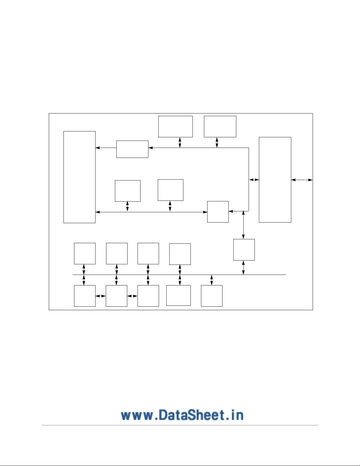
1.1 Block Diagram
Figure 1 is a block diagram of the MPC555.
Burst
Interface
RCPU
16 Kbytes
SRAM
QADC QADC QSMCM
L-bus
256 Kbytes
Flash
10 Kbytes
SRAM
TouCAN
192 Kbytes
Flash
U-bus
E-bus
USIU
L2U
UIMB
IMB3
TPU3
DPTRAM
TPU3 TouCAN MIOS1
Figure 1. MPC555 B lock Diagram
1.2 Key Features
The MPC555 key features are explained in the following sections.
1.2.1 Four-Bank Memory Controller
• Works with SRAM, EPROM, Flash EEPROM, and other peripherals
• Byte write enables
• 32-bit address decodes with bit masks
2 MPC555 Product Brief MOTOROLA

1.2.2 U-Bus System Interface Unit (USIU)
• Clock synthesizer
• Power management
• Reset controller
• MPC555 decrementer and time base
• Real-time clock register
• Periodic interrupt timer
• Hardware bus monitor and software watchdog timer
• Interrupt controller that supports up to eight external and eight internal interrupts
• IEEE 1149.1 JTAG test access port
• External bus interface
— 24 address pins, 32 data pins
— Supports multiple master designs
— Four-beat transfer bursts, two-clock minimum bus transactions
— Supports 5V inputs, provides 3.3-V outputs
Key Features
1.2.3 Flexible Memory Protection Unit
• Four instruction regions and four data regions
• 4-Kbyte to 16-Mbyte region size support
• Default attributes available in one global entry
• Attribute support for speculative accesses
1.2.4 448-Kbyte Flash EEPROM Memory
• One 256-Kbyte and one 192-Kbyte module
• Page read mode
• Block (32-Kbyte) erasable
• External 4.75-V to 5.25-V program and erase power supply
1.2.5 26-Kbytes of Static RAM
• One 16-Kbyte and one 10-Kbyte module
• Fast (one-clock) access
• Keep-alive power
• Soft defect detection (SDD)
1.2.6 General-Purpose I/O Support
• Address (24) and data (32) pins can be used for general-purpose I/O in single-chip mode
• Nine general-purpose I/O pins in MIOS1 unit
• Many peripheral pins can be used for general-purpose I/O when not used for primary function
• 5-V tolerant inputs/outputs
MOTOROLA MPC555 Product Brief 3

Key Features
1.2.7 Two Time Processor Units (TPU3)
• Each TPU3 module provides these features:
— A dedicated micro-engine operates independently of the RCPU
— 16 independent programmable channels and pins
— Each channel has an event register consisting of a 16-bit capture register, a 16-bit compare
register and a 16-bit comparator
— Nine pre-programmed timer functions are available
— Any channel can perform any time function
— Each timer function can be assigned to more than one channel
— Two timer count registers with programmable prescalers
— Each channel can be synchronized to one or both counters
— Selectable channel priority levels
— 5-V tolerant inputs/outputs
• 6-Kbyte dual port TPU RAM (DPTRAM) is shared by the two TPU3 modules for TPU microcode
1.2.8 18-Channel Modular I/O System (MIOS1)
• Ten double action submodules (DASM)
• Eight dedicated PWM sub-modules (PWMSM)
• Two 16-bit modulus counter submodules (MCSM)
• Two parallel port I/O submodules (PIOSM)
• 5-V tolerant inputs/outputs
1.2.9 Two Queued Analog-to-Digital Converter Modules
(QADC64)
Each QADC provides:
• Up to 16 analog input channels, using internal multiplexing
• Up to 41 total input channels, using internal and external multiplexing
• 10-bit A/D converter with internal sample/hold
• Typical conversion time of 10 µs (100,000 samples per second)
• Two conversion command queues of variable length
• Automated queue modes initiated by:
— External edge trigger/level gate
— Softwar e command
• 64 result registers
• Output data that is right- or left-justified, signed or unsigned
• 5-V reference and range
4 MPC555 Product Brief MOTOROLA

1.2.10 Two CAN 2.0B Controller Modules (TouCAN)
Each TouCAN provides these features:
• Full implementation of CAN protocol specification, version 2.0A and 2.0B
• Each module has 16 receive/transmit message buffers of 0 to 8 bytes data length
• Global ma sk register for message buffers 0 to 13
• Independent mask registers for message buffers 14 and 15
• Programmable transm it-first scheme: lowest ID or lowest buffer number
• 16-bit fre e-running timer for message time-s tamping
• Low power sleep mode with programmable wake-up on bus activity
• Programmable I/O modes
• Maskable interrupts
• Independent of the transmission medium (external transceiver is assumed)
• Open network architecture
• Multimaster concept
• High immun ity to EMI
• Short latency time for high-priority messages
• Low power sleep mode with programmable wakeup on bus activity
Key Features
1.2.11 Queued Serial Multi-Channel Module (QSMCM)
• Queued serial peripheral interface (QSPI)
— Provides full-duplex communication port for peripheral expansion or interprocessor
communication
— Up to 32 preprogrammed transfers, reducing overhead
— 160-byte queue buffer
— Programmable transfer length: from 8 to 16 bits, inclusive
— Synchronous interface with baud rate of up to system clock divided by 4
— Four programmable peripheral-select pins support up to 16 devices
— Wrap-around mode allows continuous sampling for efficient interfacing to serial peripherals
(e.g., – serial A/D converters, I/O latches, etc.)
• Two serial communications interfaces (SCI). Each SCI offers these features:
— UART mode provides NRZ format and half-or full-duplex interface
— 16 register receive buffer and 16 register transmit buffer (SCI1 only)
— Advanced error detection and optional parity generation and detection
— Word length programmable as 8 or 9 bits
— Separate transmitter and receiver enable bits and double buffering of data
— Wakeup functions allo w the CPU to run uni nterr upted until eithe r a tr ue idl e lin e is de tect ed or
a new address byte is received
— External source clock for baud generation
— Multiplexing of transmit data pins with discrete outputs and receive data pins with discrete
inputs, allowing realization of a low-speed serial protocol
MOTOROLA MPC555 Product Brief 5

Key Features
2 MPC555 Address Map
The internal memory map is shown in Figure 2.
0x00 0000
0x04 0000
0x06 FFFF
0x07 0000
BFFF
0x2F
0x2F C000
0x2F
FFFF
0x30 0000
7
0x30
0x30 8000
FFF
CMF Flash A
Kbytes
256
CMF Flash B
Kbytes
192
Reserved for Flash
(2.6 Mbytes - 16 Kbytes)
USIU & Flash
16 Kbytes
UIMB Interface &
IMB3 Modules
(32 Kbytes)
Control
USIU Control Registers
1
Kbyte
FLASH Module A (64 bytes)
FLASH Module B (64 bytes)
Reserved for USIU
IMB3 Address Space
DPTRAM Control
(12 bytes)
Reserved (8180 bytes)
DPTRAM (6 Kbytes)
0x2F C000
0x2F C800
0x2F C840
2F C880
0x
0x30 0000
0x30 2000
0x37 FFFF
0x38 0000
0x38 0008
0x38 0010
0x3F 9800
0x3F C000
0x 3F
FFFF
Reserved for IMB3
(4 8 0 Kbytes)
SRAM Control A
(
8
bytes)
SRAM Control B
(
8 bytes)
Reserved
(485.98 Kbytes)
SRAM A
(10 Kbytes)
SRAM B
(16 Kbytes)
Figure 2. MPC555 Internal Memory Map
Reserved (2 Kbytes)
TPU3_A (1 Kbyte)
TPU3_B (1 Kbyte)
QADC_A (1 Kbyte)
QADC_B (1 Kbyte)
QSMCM (4 Kbytes)
MIOS1 (4 Kbytes)
TouCAN_A (1 Kbyte)
TouCAN_B (1 Kbyte)
Reserved (1920 bytes)
UIMB Registers
(128 bytes)
0x30 4000
0x30 4400
0x30 4800
0x30 4C00
0x30 5000
0x30 6000
0x30 7080
0x30 7480
0x30 7884
0x30 7F80
0x30 7FFF
6 MPC555 Product Brief MOTOROLA

3 MPC555 Pinout Diagram
Figure 3 shows the pinout for the MPC555.
Key Features
3
31
0MDA
3
A
DA29 MD
A27 M
G1 MD
I
R
T
A5 E
Q
P
N57_
4BA
QA
N56_P
BA
PQA1
_
3
5
N
A
QB5 B
_P
7 BAN49
A
9_PQ
AAN5
QA4
56_P
N
A
A
PQB7
N51_
B2 AA
2_PQ
AAN
3 VDDA
1
H
C
U
P
9A_T
UCH
_TP
A
CH7
TPU
3A_
TPUCH
2CLK A_
A_T
15
H
C
TPU
B_
C
M
PW
M
PWM19 MPIO6
M
17
PWM1 MPWM2
M
MPWM
0
PWM
DL M
PUCH2 A_TPUCH5 VDDI VSSA AAN1_PQ B1 AAN50_PQB6 AAN55_PQA3 AAN58_PQA6 BAN50_PQB 6BAN55_PQA3 BAN58_PQA6 BAN59_PQA7 VDDI VDDL
T
VD
14
PUCH0 A_
PUCH
T
PUCH13 A_
PUCH10 B_T
T
T
CH7 B_
PUCH11 B_
TPU
T
_
B
B_
E
D
PIO12
M
O11
PIO7 MPIO9
M
MPI
18
M
PW
M
16
M
PIO5 MPIO8
M
CH9
TPU
4B_
H
C
PUCH8 B_TPUCH12 MPW
T
TPU
3B_
H
CH2 B_TPUC
U
PUCH5 B_TPUCH6 B_
P
T
T
_
B_
B
F
B_TPUCH1 B_TPUCH0 B_CNRX0 B_CNTX0 MPIO10 MP IO15 MPIO14 MPIO 1 3
G
H
DA28
M
3 VDDH
1
920
A
1
DA12 MD
DA15 VDDH
M
718
A11 M
1
RIG2 MDA14
T
B7 VDDH MD
Q
P
N51_
BA
PQB3
AN3_
B
_PQB2
BAN2
0
QB
P
N0_
2BA
A
11 12 13 14 15 16
4_PQ
AAN5
QA0
0
1
52_P
N
A
A
MPC555 Ball Map
PQB4
9
N48_
B0 AA
0_PQ
VRL AAN
5
1
H
C
U
P
A_T
12
_TPUCH
A
CH8
TPU
4A_
PUCH6 A_TPUCH10 A_TPUCH11 A_TPUCH14 VRH AAN3_PQB3 AAN49_PQB5 AAN53_PQA1 AAN57_PQA5 BAN1_PQB1 BAN48_PQB4 BAN52_PQA0 BAN54_PQA2 E
TPUCH
T
A_
H1
A_TPUC
12345678
VDDH
B_T2CLK VDDH A_
B
A
Figure 3. MPC555 Pinout Diagram
0
PIO1
RX
M
1 _
_CN
F
A
_CNTX0
A
VF0 _MPIO0 V
VFLS1
VFLS0
_MPIO4
_MPIO3
L
D
D
2 _MPIO2
F
VSS V
VSS
S VSS
_ QGP6
QGPO
OSI _QGP5
M
MISO _QGP4
S0
PC
_QGP
CS1
P
_QGP
VSS VSS VSS VSS
TXD2_
SCK
ECK
RXD2_ QGPI
PCS2
_QGP
QGPO
TXD1_
D1_
QGPI
PCS3
_QGP
RX
SS
he package.
t
of
w
VSS V
op down vie
t
is a
S VSS
The pinout
:
VS
Note
B
DL VS
VD
Z
FR
_
P
G
TRST_B VDD SRAM VSS VSS VSS VSS V
SDI S
DO
S
TDO_
D
TMS TDI_D
CK_ DSCK
T
J
K
SGP_
_SGP
IRQ4
IRQOUTB
GP
Q3B
S
_
_SGP
IRQ2B
IR
0 _VFLS
_SGP
IRQ1B
WP
P
LS I
VF
_
1
P
IW
L
[0] BRB_IWP2 BGB_LWP1 BBB _IWP3
G
T
S
_
WEB_ A
IRQ0B
N
M
DDH
V
F
S
S
V
CS0B VPP EPEE
]
2] WEB_ AT[3
AT[
WEB_
]
1
T[
B_ A
E
W
P
DSYN
VD
L VDDF XFC
VDD
1 VDDL VDDI KAPWR VSSSYN EXTAL
BCS1B
Z
S2
SI
T
BC
3
CS
B
WR
OEB TEAB
RD_
R
T
BUCK XTAL
_
K
CLK EC
EXT
_TXP
CFB
20 R
P
G
S
DDL Data_
V
23
P
SG
a_
t
SGP25 Da
ata_
D
a_ SGP27
t
a
D
GP29
S
GP29 VDDL Data_
S
_
r
28 Add
P
G
S
ddr_
A
_ SGP30
r
GP31 Add
S
IAddr_
BVDD
BBDIP
TAB TS
Z0
TSI
U
SETB
H HRE
wer
po
10.2
n
ersio
V
=Misc
_SGP VDD
B
Q5
R
SGP17 I
a_
t
15 Da
P
G
S
a_ SGP13 Data_
t
a
D
SGP11
a_
t
9Da
P
G
S
a_
t
7Da
P
ata_ SG
D
GP5
S
a_
t
a
D
3
P
G
S
r
powe
t
vol
ound VDDH =5
gr
=
1997
r
vembe
o
21 N
a_ SGP1 Data_
t
a
D
26
P
G
S
23 Addr_
P
GP20 Addr_ SG
S
18 Addr_
P
G
S
SGP16 Addr_
ddr_
A
GP14
S
_
r
HAdd
DD
SGP12 V
_
r
BURSTB BIB_STSB Addr_ SGP 11 Addr_ SGP10 Addr_ SGP9 Addr_ SGP8 Addr_ SGP22 Addr_ SGP27 Data_ SGP31 Data_ SGP30 Data_ SGP28 Data_ SGP26 Data_ SGP24 Data_ SGP22 Data_ SGP21 Data_ SGP19 Data_ SGP18 CLKOUT PORESETB SRESETB
dd
A
V
W
VDDH Addr_ SGP13 Addr_ SGP15 Addr_ SGP17 Addr_ SGP19 Addr_ SGP21 Addr_ SGP24 Addr_ SGP25 Data_ SGP0 Data_ SGP2 D ata_ SG P 4 Data_ SGP6 Data_ SGP8 Data_ SGP10 Data_ SGP12 Data_ SGP14 Data_ SGP16 IRQ6B _mck2 IRQ7B _mck3 VDDH
Y
)VSS
rnal
te
(in
wer
po
t
l
o
3 v
=
DDi
V
)
(I/O
r
a
powe
/97
lt
vo
/30
=3
te 9
ra
H
bst
VDD
Su
Dees
MOTOROLA MPC555 Product Brief 7

Key Features
4 Supporting Documentation List
This list contains references to currently available and planned documentation.
• MPC555 User’s Manual (MPC555UM/AD)
• RCPU Reference Manual (RCPURM/AD)
• Board Strategies for Ensuring Optimum Frequency Synthesizer Performance (AN1282/D)
• Using the MIOS on the MPC555 Evaluation Board (AN1778/D)
• Exception Table Relocation and Multi-Processor Address Mapping in the Embedded MPC5XX
Family (AN1821/D)
• Non-Volatile Memory Technology Overview (AN1837/D)
• Designing Expansion Boards for the Motorola EVB555/ETAS ES200 (AN2001/D)
• MPC555 Interrupts (AN2109/D)
• EMC Guidelines for MPC500-Based Automotive Powertrain Systems (AN2127/D)
• Nexus Standard Specification (non-Motorola document)
• Nexus Web Site: http://www.nexus5001.org/
• IEEE 1149.1 Specification (non-Motorola document)
5 Revision History
Table 2. Revision History
Revision Number Substantive Changes Date of Release
2 Existing Document. September 2001
2.1 Added temperature range for suffix A device. 11 December 2002
3 Updated template and formats. 11 February 2003
8 MPC555 Product Brief MOTOROLA

THIS PAGE INTENTIONALLY LEFT BLANK
Key Features
MOTOROLA MPC555 Product Brief 9

Key Features
THIS PAGE INTENTIONALLY LEFT BLANK
10 MPC555 Product Brief MOTOROLA

THIS PAGE INTENTIONALLY LEFT BLANK
Key Features
MOTOROLA MPC555 Product Brief 11

HOW TO REACH US:
USA/EUROPE/LOCATIONS NOT LISTED:
Motorola Literature Distribution
P.O. Box 5405, Denver, Colorado 80217
1-303-675-2140 or 1-800-441-2447
JAPAN:
Motorola Japan Ltd.
SPS, Technical Information Center
3-20-1, Minami-Azabu Minato-ku
Tokyo 106-8573 Japan
81-3-3440-3569
ASIA/PACIFIC:
Motorola Semiconductors H.K. Ltd.
Silicon Harbour Centre, 2 Dai King Street
Tai Po Industrial Estate, Tai Po, N.T., Hong Kong
852-26668334
TECHNICAL INFORMA TION CENTER:
1-800-521-6274
HOME PAGE:
http://www.motorola.com/semiconductors
Information in this document is provided solely to enable system and software implementers to use
Motorola products. There are no express or implied copyright licenses granted hereunder to design
or fabricate any integrated circuits or integrated circuits based on the information in this document.
Motorola reserves the right to make changes without further notice to any products herein.
Motorola makes no warranty, representation or guarantee regarding the suitability of its products
for any particular purpose, nor does Motorola assume any liability arising out of the application or
use of any product or circuit, and specifically disclaims any and all liability, including without
limitation consequential or incidental damages. “Typical” parameters which may be provided in
Motorola data sheets and/or specifications can and do v ary in different applications and actual
performance may vary over time. All operating parameters, including “Typicals” must be validated
for each customer application by customer’s technical experts. Motorola does not convey any
license under its patent rights nor the rights of others. Motorola products are not designed,
intended, or authorized for use as components in systems intended for surgical implant into the
body, or other applications intended to support or sustain life, or for any other application in which
the failure of the Motorola product could create a situation where personal injury or death may
occur . S h oul d Buy e r pu r cha s e or use Mot o ro la pr od uc t s fo r any s uc h uni nt e nde d or un a ut h or iz ed
application, Buyer shall indemnify and hold Motorola and its officers, employees, subsidiaries,
affiliates, and distributors harmless against all claims, costs, damages, and expenses, and
reasonable attorney fees arising out of, directly or indirectly, any claim of personal injury or death
associated with such unintended or unauthorized use, even if such claim alleges that Motorola was
negligent regarding the design or manufacture of the part.
Motorola and the Stylized M Logo are registered in the U.S. Patent and Trademark Office.
digital dna is a trademark of Motorola, Inc. The described product contains a PowerPC processor
core. The PowerPC name is a trademark of IBM Corp. and used under license. All other product
or service names are the property of their respective owners. Motorola, Inc. is an Equal
Opportunity/Affirmative Action Employer.
© Motorola, Inc. 2003
MPC555PB/D
 Loading...