

Page 1

查询MPC2605供应商
MOTOROLA
SEMICONDUCTOR TECHNICAL DATA
Product Preview
Integrated Secondary Cache
for PowerPC Microprocessors
The MPC2605 is a single chip, 256KB integrated look–aside cache with
copy–back capability designed for PowerPC applications (MPC603 and
MPC604). Using 0.38 µm technology along with standard cell logic technology ,
the MPC2605 integrates data, tag, host interface, and least recently used (LRU)
memory with a cache controller to provide a 256KB, 512KB, or 1 MB Level 2
cache with one, two, or four chips on a 64–bit PowerPC bus.
• Single Chip L2 Cache for PowerPC
• 66 MHz Zero Wait State Performance (2–1–1–1 Burst)
• Four–Way Set Associative Cache Design
• 32K x 72 Data Memory Array
• 8K x 18 Tag Array
• Address Parity Support
• LRU Cache Control Logic
• Copy–Back or Write–Through Modes of Operation
• Copy–Back Buffer for Improved Performance
• Single 3.3 V Power Supply
• 5 V Tolerant I/O
• One, Two, or Four Chip Cache Solution (256KB, 512KB, or 1MB)
• Single Clock Operation
• Compliant with IEEE Standard 1 149.1 Test Access Port (JTAG)
• Supports up to Four Processors in a Shared Cache Configuration
• High Board Density 25 mm 241 PBGA Package
BLOCK DIAGRAM
Order this document
by MPC2605/D
MPC2605
ZP PACKAGE
PBGA
CASE 1138–01
COPY–BACK
BUFFER
CONTROL
RD/WR
60X BUS
INTERFACE
A0 – A31
The PowerPC name is a trademark of IBM Corp., used under license therefrom.
This document contains information on a product under development. Motorola reserves the right to change or discontinue this product without notice.
REV 6
2/26/98
CONTROLLER
AND
BUS INTERFACE
2K x 8 LRU
A27, A28
RD/WR
8K x 72 x 4
DATA RAM
2K x 18 x 4
TAG RAM
WAY SELECT
COMPARE
DH0 – DH31
DL0 – DL31
DP0 – DP7
Motorola, Inc. 1998
MOTOROLA
MPC2605
1
Page 2

PIN ASSIGNMENT
67
A
B
C
D
L2 BR
E
F
G
ARTRY
H
J
HRESET
K
L
M
ABB
L2 BG
CPU3BGCFG4 L2
FDN
TA
CPU
DBG
TEA
TT1
TT4
TT3
MISS INH
CPU3
BR
CPU2
BR
L2 DBG
L2 CLAIM
CI AACK
CPU
BR
DBB
TT0
TT2
CPU BG
CPU3
DBG
CPU2
DBG
CPU2
BG
NC
WT
PWRDN
TBST
CLK
TS
DH19 DH29
DH20
DH23
V
DD
V
SS
V
SS
DD
DD
DD
SS
DH17
DH18
DH21
DH22
DP2 DP3
DH31
DH16
8543219
DH27
DH28
DH30
V
SS
V
SS
V
SS
V
V
SS
DD
V
V
DD
DD
V
V
DD
DD
V
V
DD
SS
V
V
SS
SS
V
V
SS
SS
DL16 DL19 DP6
DH25 DL17 DL20 DL23
DH24
DL18 DL21 V
V
V
DD
DD
V
V
DD
SS
V
V
SS
SS
V
V
SS
SS
V
V
SS
DD
V
V
DD
DD
DL22DH26
V
SS
V
V
SS
SS
V
SS
V
SS
V
DD
V
DD
V
DD
DL24
SS
15 16
DL25
DL26
V
DD
DL27
DL28
V
DD
V
SS
V
SS
V
DD
V
DD
V
DD
V
SS
171413121110 18
DL29 DL30
DL31
DP7
AP2
AP3
L2
AP0
FLUSH
APEN
CFG3
TSIZ1
TSIZ0
V
V
SS
SS
A14
A15
A18A19 A17V
A22A20 A21V
A24A25 A23V
A27A28 A26V
19
APE
AP1
L2 CI
GBL
TSIZ2
A13
A16
N
P
R
T
U
V
W
SRESET
TDI
TDO
CPU4
BG
CPU4
BR
CFG2
L2 UPDATE
L2
TAG CLR
TCK
TMS
TRST
CPU4
DBG
CFG0
CFG1
DP0 DH6 DL13
INH
NC
V
DD
V
DD
DH7
V
SS
V
V
V
SS
VSSVSSVSSDH14 DH10 DL1 DL4 V
V
DD
DH3
DH5
DH4
DH0 DH15 DH12 DH9 DH8 DL2 DL5 DL7 DL8 DL9 DL11DH2
SS
DD
V
DD
DD
SS
SS
SSVSSVSSVDD
V
V
V
V
SS
DP5
TOP VIEW (X–RAY VIEW)
V
DD
V
DD
DL15DH1 DP1 DH13 DH11 DL0 DL3 DL6 DP4 DL10 DL12 DL14
A30A31 A29
A11A10 A12
A8A7 A9
A5
A6
A3
A4
A2
A1
A0
MPC2605
2
MOTOROLA
Page 3

PIN DESCRIPTIONS
Pin Locations Pin Name Type Description
19G, 17H – 19H, 17J – 19J,
17K – 19K, 17L – 19L,
17M – 19M, 17N – 19N,
17P – 19P, 17R – 19R,
18T, 19T, 18U, 19U,
18V, 19V, 18W
3G AACK I/O Address acknowledge input/output.
2A ABB I/O Used as an input to qualify bus grants. Driven as an output during address tenure
17C – 19C, 17D *
A0 – A31 I/O Address inputs from processor. Can also be outputs for processor snoop
addresses. A0 is the MSB. A31 is the LSB.
*
initiated by the MPC2605.
AP0 – AP3 I/O Address parity.
19B APE O Address parity error. When an address parity error is detected, APE will be driven
18E APEN I Address parity enable. When tied low, enables address parity bits and the
1G ARTRY I/O Address retry status I/O. Generated when a read or write snoop to a dirty
2U
2V
1V
17E
2B
2G CI I/O Cache inhibit I/O.
3M CLK I Clock input. This must be the same as the processor clock input.
2M CPU BG I CPU bus grant input.
3E CPU2 BG I MPC2605 logically ORs this signal with CPU BG. Used in multiprocessor
1B CPU3 BG I MPC2605 logically ORs this signal with CPU BG. Used in multiprocessor
1T CPU4 BG I MPC2605 logically ORs this signal with CPU BG. Used in multiprocessor
2H CPU BR I CPU bus request input.
2D CPU2 BR I MPC2605 logically ORs this signal with CPU BR. Used in multiprocessor
2C CPU3 BR I MPC2605 logically ORs this signal with CPU BR. Used in multiprocessor
1U CPU4 BR I MPC2605 logically ORs this signal with CPU BR. Used in multiprocessor
1F CPU DBG I CPU data bus grant input from arbiter.
3D CPU2 DBG I MPC2605 logically ORs this signal with CPU DBG. Used in multiprocessor
3C CPU3 DBG I MPC2605 logically ORs this signal with CPU DBG. Used in multiprocessor
*See pin diagram (page 2) for specific pin assignment of these bus signals.
CFG0
CFG1
CFG2
CFG3
CFG4
low one clock cycle after the assertion of TS
address parity error bit.
processor cache line has occurred.
I Configuration inputs. These must be tied to either VDD or VSS.
CFG0
0 0 0 256KB
0 1 0 512KB; A26 = 0
0 1 1 512KB; A26 = 1
1 0 0 1MB; A25 – A26 = 00
1 0 1 1MB; A25 – A26 = 01
1 1 0 1MB; A25 – A26 = 10
1 1 1 1MB; A25 – A26 = 11
CFG3 Snoop Data Tenure Selector
CFG4 AACK
configuration as the second CPU BG
configuration as the third CPU BG
configuration as the fourth CPU BG
configuration as the second CPU BR
configuration as the third CPU BR
configuration as the fourth CPU BR
configuration as the second CPU DBG
configuration as the third CPU DBG
then High–Z following clock cycle.
CFG1 CFG2
0 Supports snoop data tenure
1 Does not support snoop data tenure
Driver Enable
0 Disable AACK
1 Enable AACK
driver
driver
.
.
.
.
.
.
.
.
MOTOROLA
MPC2605
3
Page 4

Pin Locations Pin Name
2T CPU4 DBG I MPC2605 logically ORs this signal with CPU DBG. Used in multiprocessor
11A – 13A, 15A – 18A,
11B – 17B, 11C, 12C, 10U,
11U, 10V – 12V, 14V – 17V,
11W – 17W
4A – 10A, 4B – 10B, 6C,
10C, 8U, 9U, 3V – 6V,
8V, 9V, 3W –10W *
14A, 18B, 5C, 8C,
16U, 7V , 13V, 2W
*See pin diagram (page 2) for specific pin assignment of these bus signals.
*
2J DBB I/O Data bus busy. Used as input when processor is master , driven as an output after
*
1C FDN I/O Flush done I/O used for communication between other MPC2605 devices. Must
19E GBL O Global transaction. Always negated when MPC2604 is bus master.
1J HRESET I Hard reset input from processor bus. This is an asynchronous input that must be
3A L2 BG I Bus grant input from arbiter.
1D L2 BR I/O Bus request I/O. Normally used as an output.
19D L2 CI I Secondary cache inhibit sampled, after assertion of TS. Assertion prevents
2F L2 CLAIM O L2 cache claim output. Used to claim the bus for processor initiated memory
2E L2 DBG I Data bus grant input. Comes from system arbiter, used to start data tenure for
18D L2 FLUSH I Causes cache to write back dirty lines and clears all tag valid bits.
3B L2 MISS INH I Prevents line fills on misses when asserted.
2N L2 TAG CLR I Invalidates all tags and holds cache in a reset condition.
3N L2 UPDATE
3J PWRDN I Provides low power mode. Prevents address and data transitions into the RAM
1N SRESET I Soft reset input from processor bus.
1E TA I/O Transfer acknowledge status I/O from processor bus.
3K TBST I/O Transfer burst status I/O from processor bus. Used to distinguish between
2P TCK I T est clock input for IEEE 1149.1 boundary scan (JTAG).
1P TDI I Test data input for IEEE 1 149.1 boundary scan (JTAG).
1R TDO O Test data output for IEEE 1149.1 boundary scan (JTAG).
1H TEA I Transfer error acknowledge status input from processor bus.
3P TMS I Test mode select for IEEE 1149.1 boundary scan (JTAG).
DL0 – DL31 I/O Data bus low input and output. DL0 is the MSB. DL31 is the LSB.
DH0 – DH31 I/O Data bus high input and output. DH0 is the MSB. DH31 is the LSB.
DP0 – DP7 I/O Data bus parity input and output.
INH
Type Description
configuration as the fourth CPU DBG
a qualified L2 DBG
L2 mode, this pin must be tied high.
be tied together between all MPC2605 parts along with a pullup resistor.
low for at least 16 clock cycles to ensure the MPC2605 is properly reset. For
proper initialization, TRST
linefill.
operations that hit the L2 cache. L2 CLAIM
of CLK following TS
resistor may be necessary to ensure proper system functioning.
bus operations where MPC2605 is the bus master.
I Cache disable. When asserted, the MPC2605 will not respond to signals on the
local bus and internal states do not change.
array. MPC2605 becomes active 4 µs after deassertion. Clock must be externally
disabled.
burstable and non–burstable memory operations.
.
when MPC2605 is the bus master. Note: To operate in Fast
must be asserted before HRESET is asserted.
goes true (low) before the rising edge
true. Because this output is not always driven, a pullup
MPC2605
4
MOTOROLA
Page 5

Pin Locations Pin Name
2R TRST I T est reset input for IEEE 1 149.1 boundary scan (JT AG). If JTAG will not be used,
3L TS I/O Transfer start I/O from processor bus (can also come from any bus master on the
17F – 19F *
1K, 2K, 1L, 2L, 1M *
3H WT I/O Write through status input from processor bus. When tied to ground, the
4C, 15C, 16C, 9D – 11D,
8H – 10H, 4J, 8J, 9J, 16J, 4K,
8K, 12K, 16K, 4L, 11L, 12L,
16L, 10M – 12M, 3T, 9T – 11T,
17T, 3U, 4U, 15U, 17U
7C, 9C, 13C, 14C, 7D, 8D,
12D, 13D, 4G, 16G – 18G,
4H, 11H, 12H, 16H, 10J – 12J,
9K – 11K, 8L – 10L, 4M,
8M, 9M, 16M, 4N, 16N, 7T, 8T,
12T, 13T, 5U – 7U, 12U – 14U
3F, 3R NC — No connection: There is no connection to the chip.
*See pin diagram (page 2) for specific pin assignment of these bus signals.
TSIZ0–TSIZ2 I/O Transfer size I/O from processor bus.
TT0–TT4 I/O Transfer type I/O from processor bus.
V
DD
V
SS
Type Description
TRST
should be tied low.
processor bus). Signals the start of either a processor or bus master cycle.
MPC2605 will operate in write–through mode only (no copy–back).
Supply Power supply: 3.3 V ± 5%.
Supply Ground.
ABSOLUTE MAXIMUM RATINGS (See Note 1)
Rating Symbol Value Unit
Power Supply Voltage V
Voltage Relative to V
Output Current (per I/O) I
Power Dissipation (Note 2) P
Temperature Under Bias T
Operating Temperature T
Storage Temperature T
NOTES:
1. Permanent device damage may occur if ABSOLUTE MAXIMUM RATINGS are
exceeded. Functional operation should be restricted to RECOMMENDED OPERATING CONDITIONS. Exposure to higher than recommended voltages for extended
periods of time could affect device reliability.
2. Power dissipation capability is dependent upon package characteristics and use
environment. See Package Thermal Characteristics.
SS
DD
Vin, V
out
bias
stg
out
D
J
– 0.5 to + 4.6 V
– 0.5 to VDD + 0.5 V
± 20 mA
— W
– 10 to + 85 °C
0 to + 125 °C
– 55 to + 125 °C
This device contains circuitry to protect the
inputs against damage due to high static voltages or electric fields; however, it is advised
that normal precautions be taken to avoid
application of any voltage higher than maximum rated voltages to this high–impedance
circuit.
This BiCMOS memory circuit has been designed to meet the dc and ac specifications
shown in the tables, after thermal equilibrium
has been established.
MOTOROLA
MPC2605
5
Page 6

DC OPERA TING CONDITIONS AND CHARACTERISTICS
(TJ = 20 to + 1 10 °C, Unless Otherwise Noted)
RECOMMENDED OPERATING CONDITIONS
Parameter
Supply Voltage (Operating Voltage Range) V
Input High Voltage V
Input Low Voltage V
*VIL(min) = – 2.0 V ac (pulse width ≤ 20 ns).
(Voltages Referenced to VSS = 0 V)
Symbol Min Typ Max Unit
DD
IH
IL
DC CHARACTERISTICS
Parameter Symbol Min Max Unit
Input Leakage Current (All Inputs, Vin = 0 to VDD) I
Output Leakage Current (High–Z State, V
AC Supply Current (I
Cycle Time = 15 ns, max value assumes a constant burst read hit, with 100% bus utilization,
and 100% hit rate)
AC Quiescent Current (I
Cycle Time = 15 ns, All Other Inputs DC)
Output Low Voltage (IOL = + 8.0 mA) V
Output High Voltage (IOH = – 4.0 mA) V
= 0 mA, All inputs = VIL or VIH, VIL = 0 V, and VIH≥ 3.0 V,
out
= 0 mA, All inputs = VIL or VIH, VIL = 0 V and VIH ≥ 3.0 V ,
out
CAPACITANCE (f = 1.0 MHz, dV = 3.0 V, T
Input Capacitance C
Output Capacitance C
Input/Output Capacitance C
= 0 to VDD) I
out
= 25°C, Periodically Sampled Rather Than 100% Tested)
A
Parameter Symbol Typ Max Unit
3.135 3.3 3.465 V
2.0 — 5.5 V
– 0.5* — 0.8 V
lkg(I)
lkg(O)
I
CCA
I
Q
OL
OH
in
out
I/O
— ± 1.0 µA
— ± 1.0 µA
— 720 mA
— 195 mA
— 0.4 V
2.4 — V
4 6 pF
6 8 pF
8 10 pF
PACKAGE THERMAL CHARACTERISTICS
Rating Symbol Max Unit
Thermal Resistance Junction to Ambient (Still Air, Test Board with Two Internal Planes) R
Thermal Resistance Junction to Ambient (200 lfpm, Test Board with Two Internal Planes) R
Thermal Resistance Junction to Board (Bottom) R
Thermal Resistance Junction to Case (Top) R
θJA
θJA
θJB
θJC
26.5 °C/W
23.2 °C/W
15.9 °C/W
6.6 °C/W
MPC2605
6
MOTOROLA
Page 7

AC OPERA TING CONDITIONS AND CHARACTERISTICS
Timing
(TJ = 20 to + 1 10 °C, Unless Otherwise Noted)
Input Timing Measurement Reference Level 1.5 V. . . . . . . . . . . . . . .
Input Pulse Levels 0 to 3.0 V. . . . . . . . . . . . . . . . . . . . . . . . . . . . . . . . .
Input Rise/Fall Time 2 ns. . . . . . . . . . . . . . . . . . . . . . . . . . . . . . . . . . . .
Output Measurement Timing Level 1.5 V. . . . . . . . . . . . . . . . . . . . . . .
Output Load 50 Ω T ermination to 1.5 V. . . . . . . . . . . . . . . . . . . . . . . .
AC CLOCK SPECIFICATIONS
Timing
Parameter
Frequency of Operation — 66.67 MHz
Clock Cycle Time
Clock Rise and Fall Time
Clock Duty Cycle Measured at 1.5 V 40 60 %
Clock Short–Term Jitter (Cycle to Cycle) — ± 150 ps 1
NOTES:
1. This parameter is sampled and not 100% tested.
2. Rise and fall times for the clock input are measured from 0.4 to 2.4 V .
Reference
,
MPC2605–66
Min Max
15 — ns
1.0 2.0 ns 1, 2
Unit Notes
CLOCK INPUT TIMING DIAGRAM
VM
VM = Midpoint Voltage (1.5 V)
V
IH
V
IL
MOTOROLA
MPC2605
7
Page 8

AC SPECIFICATIONS
Timing
Timing
Parameter
Clock Cycle Time
Input Setup Time
Clock to Input Invalid (Input Hold)
Clock to Output Driven
Clock to Output Valid
Clock to Output Invalid
Clock to Output High–Z
PWRDN Disable to Recovery — 4 µs 2
NOTES:
1. All input specifications are measured from the TTL level (0.8 or 2.0 V) of the signal in question to the 1.4 V level of the rising edge of the input
clock. Both input and output timings are measured at the pin.
2. This parameter is sampled and not 100% tested.
CLK
INPUTS
Reference
MPC2605–66
Min Max
15 — ns
4.5 — ns 1
2 — ns 1
2 9 ns 2
2 9 ns
2 — ns 2
2 12 ns 2
Unit Notes
OUTPUTS
MPC2605
8
MOTOROLA
Page 9

MPC2605 RESPONSE TO 60X TRANSFER ATTRIBUTES
TT0 – TT4 TBST CI WT Tag Status MPC2605 Response Notes
X1X10 0 1 X Miss Line–fill (processor read miss) 1, 2, 3
X1X10 0 1 X Hit L2 CLAIM, AACK, TA (processor read hit) 4
X1010 1 0 X Hit Clean Paradox — Invalidate the line (processor n–cacheable read hit
X1010 1 0 X Hit Dirty Paradox — ARTRY, L2 BR, then write back data, invalidate the line
00110 0 1 X Miss Line–fill except right after a snoop hit to processor (processor write
00110 0 1 1 Hit L2 CLAIM, AACK, TA except after a snoop hit to processor
00X10 X 1 0 Hit Clean Cache update (processor write through WT hit clean)
00110 0 1 0 Hit Dirty Cache update, clear dirty bit
00010 1 1 0 Hit Dirty Paradox — ARTRY, L2 BR, write back data, keep valid, clear dirty
X0010 1 0 X Hit Clean Paradox — Invalidate the line (processor n–cacheable write hit
X0010 1 0 X Hit Dirty Paradox — ARTRY, L2 BR, then write back data, invalidate the line
00100 X X X Hit Clean Invalidate tag (flush block address–only)
00100 X X X Hit Dirty ARTRY, L2 BR, write back data, invalidate tag (flush block
00000 X X X Hit Clean No action (clean block address–only)
00000 X X X Hit Dirty ARTRY, L2 BR, write back data, reset dirty bit (clean block
01100 X X X Hit Invalidate tag (kill block address–only)
NOTES:
1. If a line fill is going to replace a dirty line and the cast out buffer (COB) is full, the line fill will be cancelled. (Unless the line fill is a write which
hits in the COB. In this case, the line fill will occur.)
2. If a burst read misses the cache but hits the COB, the MPC2605 will supply the data from the COB, but not perform a line fill.
3. If ARTRY
dirty, tag field), and the COB goes back to an invalid condition, even if the line fill is a burst write to the line in the COB.
4. If ARTRY
5. If a processor burst write occurs right after a snoop write that was a cache hit, the MPC2605 will invalidate the line. If the snoop was a cache
miss, the MPC2605 will not perform a write allocate.
6. If a processor burst write occurs right after a snoop read that was a cache hit, the MPC2605 will update the cache and clear the dirty bit.
If the snoop was a cache miss, the MPC2605 will perform a write allocate.
is asserted during a line fill to replace a dirty line, the line fill will be cancelled, the to–be–replaced line will recover its old tag (valid,
is asserted during a read hit, the MPC2605 will abort the process.
clean line)
(processor n–cacheable read hit dirty line)
1, 3, 5, 6
miss)
(processor write hit)
bit
clean line)
(processor n–cacheable SB write hit dirty line)
address–only)
address–only)
5, 6
MPC2605 RESPONSE TO CHIPSET TRANSFER ATTRIBUTES
TT0 – TT4 Tag Status MPC2605 Response
00100
X0010
X1110
00100
X0010
X1110
00000
X1010
00000
X1010
0110X
00110
NOTE: In all snoop push cases, BR is sampled the cycle after the ARTRY window. If BR is asserted in this cycle, L2 BR will be immediately negated
and an assertion of L2 BG
Hit Clean Invalidate line
Hit Dirty ARTRY and L2 BR write back data, invalidate line (see Note)
Hit Clean No action
Hit Dirty ARTRY and L2 BR, write back data, reset dirty bit (see Note)
Hit Invalidate (kill block)
will be ignored.
TRANSFER ATTRIBUTES GENERATED FOR L2 COPYBACK
TT0 – TT4 TBST CI WT
00010 0 1 1
MOTOROLA
MPC2605
9
Page 10

FUNCTIONAL OPERATION
SYSTEM USAGE AND REQUIREMENTS
The MPC2605 is a high–performance look–aside cache
for PowerPC systems. A look–aside cache is defined as a
cache that resides on the same bus as the processor, the
memory controller, the DMA bridge, and the arbiter. The advantage of a look–aside cache is that, when the processor
makes a memory request, the cache adds no delay to the
memory controller’s response time in the event that the request cannot be satisfied by the cache. However, there are
certain system requirements that must be met before a look–
aside cache can be used.
Comprehension of L2 CLAIM
Because the memory controller sees every memory request that is issued by the processor, there must be a mechanism for the cache to inform the memory controller that it
has detected a cache hit and that it will satisfy the processor’s request. The MPC2605 has a signal called
L2 CLAIM
Any memory controller with which the MPC2605 is to be
used must have the ability to monitor this signal.
Pipeline Depth
The 60X bus allows pipelining of transactions such that a
new transaction can be initiated before a previous transaction has fully completed. The level of pipelining that exists on
the bus is defined by how many new data transactions have
been initiated while the original transaction is still being processed. By this definition the MPC2605 can only work in a
one level deep pipeline. In the presence of transactions for
which it has asserted L2 CLAIM
the level of pipelining by delaying its assertion of AACK
However, for transactions that it cannot control, the
MPC2605 is dependent upon the memory controller to control pipeline depth. Thus, another system requirement for the
use of the MPC2605 is the use of a memory controller that
only allows one level deep of pipelining on the 60X bus.
that is asserted whenever a cache hit is detected.
, the MPC2605 can control
CFG0 – CFG2
These three configuration pins are used to implement the
different cache sizes supported by the MPC2605.
256KB: For a single chip implementation, CFG0, CFG1,
and CFG2 should all be tied low.
512KB: This two chip configuration requires both parts to
have CFG0 tied low and CFG1 tied high. CFG2 is
used as a chip select when it matches the value of
A26. Therefore, one device must have CFG2 tied
low and the other device must have CFG2 tied
high.
1MB: The four chip configuration requires all four de-
vices to have CFG0 tied high. The CFG1, CFG2
vector becomes the chip select when it matches
the A25, A26 vector. Therefore, each of the four
parts must have a unique value of the CFG[1:2]
vector.
CFG3
Many core logic chipsets are designed such that the DMA
bridge and the memory controller are resident in the same
device. In such systems there is internal communication between these two functional units. Bus transactions generated
by the DMA bridge are solely for the purpose of keeping the
system coherent. They are not explicit requests from
memory that have data tenures associated with them. However, some chipsets are designed with the memory controller
and the DMA bridge partitioned into different devices. In systems such as these, transactions generated by the DMA
bridge are true memory requests that have data tenures
associated with them. These are called snoop data tenures.
Because these two types of systems are fundamentally different, the MPC2605 must know in which type of system it is
.
resident in order to respond properly to the different types of
transactions. For systems that do not have snoop data tenures, CFG3 must be tied high. For systems that do use
snoop data tenures, CFG3 must be tied low.
CFG4
Bus Mastering
Bus mastering is a requirement only for systems which
seek to use the MPC2605 as a copyback, as opposed to a
write–through, cache. The requirement is that the system arbiter must have the ability to allow the MPC2605 to become
a bus master. Specifically, the system arbiter must be able to
recognize assertions of L2 BR
assert L2 BG and L2 DBG.
These are the only requirements above and beyond what
should already exist in a PowerPC system. All other necessary control signals are signals that are required for the processor to communicate with the memory controller, the DMA
bridge, and the arbiter.
CONFIGURATION PINS
The MPC2605 has five configuration pins: CFG0, CFG1,
CFG2, CFG3, and CFG4.
and must have the ability to
MPC2605
10
When the MPC2605 asserts L2 CLAIM
memory controller that a cache hit has been detected, it is
taking control of the address and data tenures of the transaction (see 60X Bus Operation and Memory Coherence).
This means that the MPC2605 will assert AACK
address tenure, and it will assert TA as needed for the data
tenure. If the data bus is idle when a processor request is initiated, the MPC2605 will assert AACK
asserted. If the data bus is busy when the request is made,
the MPC2605 will wait until the outstanding data tenure has
completed before asserting AACK
assertion of AACK
most, two outstanding data transactions at any one time. Tying CFG4 low prevents the MPC2605 from asserting AACK
to end transactions for which it has asserted L2 CLAIM. In
systems that tie CFG4 low it is necessary for the memory
controller to assert AACK
DMA bridge to initiate snoop transactions (as defined later)
even when there are two outstanding data transactions. If
this type of system is implemented, the arbiter must ensure
, the MPC2605 enforces the policy of, at
for all transactions. This allows the
to signal to the
to end the
the cycle after TS was
. By holding off on the
MOTOROLA
Page 11

that the processor’s bus grant is negated once there are two
outstanding data transactions. It is expected that most systems will tie CFG4 high.
RESET/INITIALIZATION
To ensure proper initialization and system functionality, the
HRESET pin of the MPC2605 should be connected to the
same signal that is used to reset the processor. The TRST
signal must be negated before HRESET is negated. When
HRESET
initialization sequence to clear all of the valid bits in the
cache. The sequence takes approximately 4000 clock
cycles. During this time the MPC2605 will not participate in
any bus transaction that occurs. All transactions are, however, monitored so that, regardless of when the initialization sequence completes, the MPC2605 is prepared to take action
on the next transaction initiated by the processor.
MPC2605 will detect its first cache hit. At this time the system
will experience its first assertion of L2 CLAIM
controller must be configured via software to comprehend
assertions of L2 CLAIM
have completed by this time. For systems that cannot guarantee that this requirement is met, it is necessary to disable
the MPC2605 until such time as this configuration can be
guaranteed. Disabling the MPC2605 can be accomplished
by asserting L2 UPDA TE INH
gating it when it is deemed safe for caching to commence.
60X BUS OPERATION
address tenure is a set number of bus cycles during which
the address bus and its associated control signals are being
used for the transaction at hand. In general, there are two
types of transactions. Those that only have address tenures,
called address–only transactions. And those that require the
use of the data bus and therefore will have a data tenure.
These transactions are called data transactions. This section
describes how address and data tenures are defined as
viewed by the MPC2605.
Address T enures
They start with an assertion of TS
granted the bus by the system arbiter. This device is called
the bus master for this transaction. At the same time that TS
is asserted, the bus master also drives the address and all
other relevant control signals that define the transaction. TS
is only asserted for one cycle but all other signals are held
valid by the bus master until some other device asserts
AACK
this transaction. Typically, the slave is the memory controller,
although for transactions that are cache hits the MPC2605
becomes the slave by driving L2 CLAIM
asserting ARTRY
TS is asserted, but must be held through the cycle after
AACK
window, since it is the cycle in which all devices sample
ARTRY
successfully.
is negated, the MPC2605 commences an internal
At some point after this 4000 cycle sequence, the
. If the memory
, this configuration operation must
sometime during reset and ne-
All transactions have what is called an address tenure. An
Address tenures on the 60X bus are fairly well defined.
by a device that has been
. The device that asserts AACK becomes the slave to
.
Transactions can be aborted by any device on the bus by
. ARTRY may be asserted at any time after
is asserted. This cycle is referred to as the ARTRY
to determine if the address tenure has completed
If an address tenure is not aborted by an assertion of
ARTRY
, then the next bus master is free to assert TS, the
cycle after the ARTRY window to start a new address tenure.
If ARTRY
are not asserting ARTRY
the following cycle. This next cycle is called the BR window.
The purpose of this protocol is to give immediate bus mastership to the device that asserted ARTRY
that that device will take this opportunity to clean up whatever circumstances caused it to assert ARTRY
involves writing data back to memory to maintain coherence
in the system.
Data Tenures
tenures. They require two conditions to start: an assertion of
TS
of the bus master’s data bus grant. For a data bus grant to be
considered qualified, no device on the bus may be asserting
DBB
tions and burst transactions. The type is determined by the
state of TBST
the bus master asserts TBST
action and will require four assertions of TA in order to complete normally . If TBST
the transaction only requires one assertion of TA
name single–beat.
depends upon whether the transaction is a read or a write.
For a read transaction, the slave device drives the data bus.
For a write transaction, the master drives the data bus. In all
data transactions, the slave device asserts TA
that either valid data is present on the bus, in the case of a
read; or that it is reading data off the data bus, in the case of
a write. The master device asserts DBB
been granted the data bus and keeps it asserted until the
data tenure has completed.
address tenure for the transaction can be aborted by an
assertion of ARTRY
indicate that some error condition has been detected. Either
event will prematurely terminate the data tenure.
Data Streaming
state between the completion of one data tenure and the
start of the next. This turnaround cycle avoids the contention
on the data bus that would occur if one device starts driving
data before another device has had a chance to turn off its
data bus drivers. When a cache read hit is pipelined on top of
another cache read hit, there is no need for this turnaround
cycle since the same device will be driving the data bus for
both data tenures. The 60X bus has the ability to remove this
unnecessary wait state and allow back–to–back cache read
hits to stream together. This ability is only enabled if the system is put into Fast L2 mode. Note that not all PowerPC processors support Fast L2 mode.
streaming capability is that the system arbiter must be
sophisticated enough to identify situations in which streaming may occur. Upon recognizing these situations, it must assert the processor’s data bus grant in the cycle coincident
is asserted in the ARTRY window, all devices that
must negate their bus request in
with the expectation
. Typically, this
Data tenures are more complicated to define than address
that initiates a data transaction and a qualified assertion
in the cycle that the data bus grant is asserted.
Data transactions come in two types: single–beat transac-
during the address tenure of the transaction. If
, the transaction is a burst trans-
is negated during the address tenure,
, thus the
Which device drives the data bus during a data transaction
to indicate
the cycle after it has
A data tenure can be aborted in two different ways. The
. Or, the slave device may assert TEA to
For the majority of data transactions there must be a wait
One of the requirements for taking advantage of this data
MOTOROLA
MPC2605
11
Page 12

with the fourth assertion of T A of the first cache read, so that
the data tenure for the second cache read may commence in
the next cycle.
Because it only recognizes qualified assertions of
CPU DBG
sor’s assertions of DBB
MPC2605 must be tied to a pullup resistor rather than connected to the system DBB
connected. This forces the system arbiter to a level of sophistication such that it only supplies qualified data bus
grants and thus the DBB
system.
Note: In a multi–chip configuration each MPC2605 device
acts as an independent cache. Zero wait state data streaming can only occur if the back to back read hits occur in a given device. If the second read hit is not in the device as the
first read hit, a wait state will occur between the two data tenures (2–1–1–1–2–1–1–1 timing).
Data Bus Parking
The MPC2605 has the ability to respond to a processor
read or write hit starting in the cycle after the processor has
asserted TS
However, even though the MPC2605 has this ability, it is dependent upon the system to allow this quick of a response to
occur. As discussed above, a data tenure cannot start until
the master has been given a qualified bus grant. In order for
the data tenure to start the cycle after TS
data bus must be granted in the cycle coincident with the
assertion of TS
cult for an arbiter to detect an assertion of TS
sert CPU DBG in the same cycle. In order to realistically
allow this situation to occur, CPU DBG
dependent of the processor’s assertion of TS.
Data bus parking is a system feature whereby the processor always has a qualified data bus grant when the data bus
is idle. It is also a requirement for systems which seek to take
advantage of the 2–1–1–1 response time capabilities of the
MPC2605. This feature is typically present in arbiters that
have the level of sophistication necessary to support data
streaming. But it is also a feature of systems that do not even
have a data bus arbiter. In these systems the data bus grant
of every device in the system is tied to ground. The assertion
of DBB
the qualified data bus grant of all devices in the system, including its own. Note that in systems that have no data bus
arbiter that it is impossible to take advantage of data streaming.
There is another caveat associated with data bus parking.
Care must be taken when using data bus parking along with
Fast L2 mode. In normal bus mode when the processor
reads data off the bus, it will wait one cycle before passing
the data on to internal functional units. The purpose of this
one cycle waiting period is to check for an assertion of
DRTRY
read. One of the advantages of running the processor in Fast
L2 mode is that this internal processor wait state is removed.
A problem will arise, however, if the processor is given
data the cycle after TS
MPC2605, and the transaction is aborted by some other device asserting ARTRY
, the MPC2605 must not be aware of the proces-
. This means that the DBB pin of the
to which all other devices are
signal is unnecessary to the whole
. This is referred to as a 2–1–1–1 response.
is asserted, the
. At bus speeds of 66 MHz it is extremely diffi-
and itself as-
must be asserted in-
by the current data bus master effectively removes
, which invalidates the data that has been already
is asserted, as is possible with the
. Because the processor will not sam-
ple ARTRY
read off the bus will have already been forwarded to the
internal functional units. Thus, incorrect results may occur in
the system.
T o avoid this situation in a system that seeks to run Fast L2
mode with the data bus parked, there must be a guarantee
that ARTRY
is a further requirement to be imposed upon the DMA bridge
and the memory controller. If this guarantee cannot be made,
the data bus cannot be parked when running in Fast L2
mode.
Processor Reads
When the processor issues a read transaction, the
MPC2605 does a tag lookup to determine if this data is in
the cache. If there is a cache hit and CI
MPC2605 will assert L2 CLAIM
processor when the data tenure starts.
If the processor issues a cache–inhibited read (CI
serted) and the MPC2605 detects a cache hit to a non–dirty ,
or clean, cache line, the line will be marked invalid. If the
cache–inhibited read hits a dirty line, the MPC2605 will assert ARTRY
If the read misses in the cache, the MPC2605 will perform
a linefill only if it is a burst read and it is not marked cache–inhibited. During a linefill, the MPC2605 stores the data present on the bus as it is supplied by the memory controller.
Processor Writes
The conditions for asserting L2 CLAIM
are almost the same as for processor reads. There must be a
cache hit and CI
must not be asserted. Single beat writes that are marked
WT
either write–through or cache–inhibited that hit in the cache
cause the MPC2605 to assert ARTRY
back to memory .
Transaction Pipelining
As explained in Pipeline Depth, the MPC2605 can only
handle one level of pipelining on the bus. Since the assertion
of L2 CLAIM
MPC2605 has the ability to control this pipeline depth for
transactions that are cache hits by delaying its assertion of
AACK
Pipelined cache hits are transactions that hit in the cache
but occur while there is still an outstanding data transaction
on the bus. The timing of the assertion of AACK
lined cache hit is dependent upon the completion of the previous transaction. For explanation purposes, the previous
transaction will be referred to as transaction one. The pipelined cache hit will be referred to as transaction two.
If transaction one is a cache hit, the MPC2605 will be the
slave device for the transaction. Since, for burst operations,
the MPC2605 always asserts TA
cycles, the end of the data tenure for transaction one will be
at a deterministic clock cycle. In this case, AACK
tion two can be asserted coincident with the last assertion of
for transaction one. If transaction one is not a cache hit,
TA
the MPC2605 will wait until after the data tenure for transaction one has completed before asserting AACK
the address tenure of transaction two.
until two cycles after the assertion of TS, the data
will never be asserted for cache read hits. This
is not asserted, the
and supply the data to the
as-
and write the dirty line back to memory .
for processor writes
must not be asserted. In addition, however,
and write the dirty line
gives it the ability to assert AACK, the
.
for a pipe-
for four consecutive clock
for transac-
to complete
MPC2605
12
MOTOROLA
Page 13

MEMORY COHERENCE
When a processor brings data into its on–chip cache and
modifies it, a situation has arisen in which the main memory
now contains irrelevant, or stale, data. Given that most systems support some form of DMA there must exist a means by
which the processor is forced to write this modified, or dirty,
data back to main memory. The DMA bridge is responsible
for generating bus transactions to ensure that main memory
locations accessed by DMA operations do not contain stale
data. These transactions, called snoops, come in three different categories, each of which will be discussed below.
Snoops cause the processor and the MPC2605 to check
to see if they have dirty copies of the memory location specified in the snoop transaction. If either device does have a
dirty copy it will assert ARTRY
nity presented in the BR window to write this data back to
main memory.
Situations can arise where a cache line is dirty in both the
processor’s L1 cache and in the MPC2605. In cases such as
these, snoop transactions should cause the processor to
write its data back to memory since it is by definition more
recent than the data in the MPC2605. Since ARTRY
shared signal and it cannot be determined which devices are
driving it, the MPC2605 samples CPU BR
to determine if the snoop hit a dirty line in the L1 cache. If
CPU BR
defer to the processor.
Snoop Reads
memory but allows both the L1 and L2 to keep a valid copy.
In cases where the snoop hits a dirty cache line in the processor, the MPC2605 will update its contents as the processor writes the data back to main memory .
the DMA bridge can issue a clean transaction (TT[0:4] =
00000). The other is that the DMA bridge can do a read
transaction (TT[0:4] = x1010). If the DMA bridge does a read
transaction, the MPC2605 determines that it is a snoop read
rather than a processor read by the state of CPU BG
cycle before TS
granted the bus then the transaction had to have been issued by the DMA bridge and is therefore a snoop read.
Snoop Writes
main memory. The difference from a snoop read is that the
cache line must then be invalidated in both the processor’s
cache and in the L2 cache. When the processor writes data
back to memory in response to a snoop write, the MPC2605
will not cache the data as it appears on the bus. If a valid
copy resides in the cache, the MPC2605 will invalidate it.
the DMA bridge to implement a snoop write. It can issue a
flush transaction (TT[0:4] = 00100), a read with intent to
modify (TT[0:4] = x1110), or a write with flush (TT[0:4]
= 00010). As with snoop reads, the MPC2605 distinguishes
between processor issued data transactions and snoop
transactions by the state of CPU BG
the assertion of TS
is asserted during this window, the MPC2605 will
A snoop read causes dirty data to be written back to
Snoop reads can be implemented in two ways. One is that
was asserted. If the processor was not
Snoop writes also cause dirty data to be written back to
Again there are multiple transactions that can be used by
.
and make use of the opportu-
is a
in the BR window
the
in the cycle previous to
Snoop Kills
Kills are snoops that cause cache entries to be immediately invalidated, regardless of whether they are dirty. This
saves time if the DMA operation is going to modify all the
data in the cache line. To implement a snoop kill the DMA
bridge can issue a kill transaction (TT[0:4] = 01 100) or a write
with kill (TT[0:4] = 001 10).
TWO/FOUR CHIP IMPLEMENTATION
Multiple Castouts
Because each MPC2605 has its own castout buffer
(COB), it is possible for situations to arise in which more than
one device needs to do a copyback operation. Under normal
circumstances each device will enter castout conditions at
different times. In these cases, when a device determines
that it needs to do a castout, the L2 BR
sampled. If L2 BR
another device is also in a castout situation. The late device
will wait until L2 BR
tempt to perform its castout.
Because of the BR window protocol associated with assertions of ARTRY
device two is waiting for device one to do its castout before
asserting L2 BR
vice other than device one, device one is required to negate
in the BR window. In order to prevent device two from
L2 BR
interpreting device one’s negation of L2 BR as an indication
that device one has completed its castout, a simple arbitration mechanism is used. All devices have a simple two–bit
counter that is synchronized such that all counters always
have the same value. For the purposes of performing a castout operation, a given pair can only assert L2 BR
er is equal to its value of CFG[1:2]. This simple mechanism
prevents more than one device from asserting L2 BR
same cycle and therefore not being cognizant of the another
device’s need to perform a castout.
Snoop Hit Before Castout
The other situation that can cause problems with a shared
bus request occurs when a snoop hits a dirty line in one of
the MPC2605 devices. If device one has a cache line in its
COB, it will assert L2 BR
operation. If a snoop hits a dirty line in device two, it will assert both ARTRY
data back to main memory. When device one detects that
has been asserted, it needs to be made aware that
ARTRY
device two needs to request the bus. Otherwise, at the same
time that device two is asserting L2 BR
tempt to conform to the BR window protocol and negate
. This situation is avoided by device one sampling FDN
L2 BR
when it detects that ARTRY has been asserted. If FDN is
asserted at the same time as ARTRY is asserted, device one
will recognize that device two is asserting ARTRY
one will then high–Z L2 BR
tion when device two is asserting L2 BR
MUL TIPROCESSING
The MPC2605 can be used as a common cache for up to
four processors. For each processor there is a bus request,
bus grant, and data bus grant signal pin on the MPC2605.
Each of these pins needs to be connected to the respective
processor’s arbitration signals in the system.
is already asserted then it is clear that
is negated before continuing in its at-
, it is possible for a situation to arise where
. If there is an assertion of ARTRY by a de-
so that it may perform a castout
and L2 BR so that it can write the snoop
so that there will not be conten-
signal is first
if the count-
in the
, device one will at-
. device
.
MOTOROLA
MPC2605
13
Page 14

The MPC2605 treats multiple processors as one processor. Thus, the same restrictions on pipelining depth are true
with regard to how many processor transactions can be outstanding at any one time. There can only be one data
transaction from ANY processor pipelined on top of a current
data transaction that was issued by ANY processor.
The data tenures for all processors must be performed in
the same order as the address tenures on a system–wide
basis. If processor one makes a request and then processor
two makes a request, processor one’s data tenure must precede processor two’s data tenure. Note that this is not a 60X
bus restriction, but rather a restriction necessary for proper
operation of the MPC2605.
The MPC2605 keeps coherent with the L1 caches of multiple processors as defined by the MESI (modified–exclusive–
shared–invalid) protocol without actually implementing the
protocol. This is possible for two reasons. Since the
MPC2605 is a look–aside cache, all transactions are monitored by all devices on the bus. Also, the MPC2605 cannot,
on its own, modify data. Thus, if one processor requests exclusive access to a cache line, it is not necessary for the
MPC2605 to invalidate its copy of the data, as would be required under the MESI protocol. If a second processor requests the same data, the transaction will cause the first
processor to assert ARTRY
from supplying stale data to the second processor.
As discussed in Data Bus Parking, care must be taken
when parking the data bus in Fast L2 mode. By the nature of
MP systems running under the MESI protocol there will be
assertions of ARTRY
MP system, the data bus cannot be parked to any processor
if the system is to be run in Fast L2 mode.
PWRDN
An assertion of PWRDN will cause the MPC2605 to go into
a low–power sleep state. This state is entered after PWRDN
is synchronized and both the address and data buses are
idle. All data is retained while in the sleep state.
The behavior of the MPC2605 upon negation of PWRDN
is dependent upon the state of WT at the rising edge of
HRESET
invalidate all cache entries when PWRDN
is negated at reset, the MPC2605 will leave all cache entries
as they were prior to the assertion of PWRDN. However, in
this situation, the system designer must insure that no bus
activity occur within two microseconds of the negation of
PWRDN
able its internal clock network. The low power state current
stated in this specification assumes that the system clock is
not toggling.
ASYNCHRONOUS SIGNALS
nals. These signals were originally defined in the PowerPC
reference platform (PReP) specification. Because these signals are defined to be asynchronous, the MPC2605 must
. If WT is asserted at reset, the MPC2605 will
.
Note: While in the sleep state the MPC2605 does not dis-
The MPC2605 supports four asynchronous control sig-
. This will prevent the MPC2605
to abort cache read hits. Thus, in an
is negated. If WT
synchronize them internally. This process takes eight clock
cycles. Thus, to guarantee recognition by the MPC2605,
assertions of any one of these signals must last a minimum
of eight clock cycles.
L2 FLUSH
When L2 FLUSH is asserted, the MPC2605 initiates an internal sequence that steps through every cache line present.
Valid lines that are clean are immediately marked invalid.
Valid lines that are dirty must be written back to main
memory.
To keep memory up to date, the MPC2605 must still monitor all transactions on the bus. Any transaction that is not a
processor burst write will cause the MPC2605 to assert
. Burst writes cause the MPC2605 to do a lookup on
ARTRY
the affected address and mark the line invalid if it is present.
Because the MPC2605 must still monitor all transactions,
it cannot use the tag RAM for the flush sequence unless
there is a guarantee that no new transaction will be initiated
on the bus. The only way to ensure that no new transactions
will occur is for the MPC2605 to be granted the bus. Thus,
upon entering the sequence initiated by the assertion of
L2 FLUSH
L2 BG
the tag RAM entries.
L2 FLUSH
quence to complete. Once started the sequence will run to
completion unless overridden by an assertion of HRESET
L2 MISS INH
When L2 MISS INH is asserted, the MPC2605 will not load
any new data into the cache. The data already present will
remain valid and the MPC2605 will respond to cache hits.
This condition only lasts as long as L2 MISS INH
When L2 MISS INH
bring new data into the cache when there are cache misses.
L2 T AG CLR
When L2 TAG CLR is asserted, the MPC2605 will invalidate all entries in the cache. This internal sequence is the
same as the one initiated by an assertion of HRESET
this sequence, the MPC2605 will not participate in any bus
transaction. However, it will keep track of all bus transactions
so that when the sequence is finished, the MPC2605 can immediately participate in the next bus transaction.
As is the case with assertions of L2 FLUSH
of L2 TAG CLR
quence. Once asserted the sequence will run to completion
regardless of the state of L2 T AG CLR
L2 UPDATE INH
When L2 UPDATE INH is asserted, the MPC2605 is
disabled from responding to cacheable transactions. Bus
transactions continue to be monitored so that as soon as
L2 UPDATE INH
in the next transaction.
, the MPC2605 will assert L2 BR. As soon as
is asserted, the MPC2605 can start stepping through
need not be held asserted for the flush se-
.
is asserted.
is negated, the MPC2605 will start to
. During
, an assertion
need not be held for the duration of the se-
.
is negated, the MPC204GA can participate
MPC2605
14
MOTOROLA
Page 15

READ HIT/WRITE HIT
Figure 1 shows a read hit from an idle bus state. The
MPC2605 asserts L2 CLAIM
the cycle after TS to inform the
memory controller that there is a cache hit and the cache will
control the rest of the transaction. L2 CLAIM
the cycle after AACK
is asserted. Since there are no active
is held through
data tenures from previous transactions, the MPC2605
asserts AACK
the cycle after TS is asserted. Note there must
123456
CLK
CPU BG
TS
be a qualified assertion of CPU DBG
assertion of TS
next cycle. CPU DBG
for the MPC2605 to respond with TA in the
does not affect the timing of L2 CLAIM
in the same cycle as the
or AACK.
The write hit timing is virtually the same. The only difference is the processor drives the data instead of the
MPC2605.
A0 – A31
TBST
L2 CLAIM
AACK
CPU DBG
DBB
TA
DH0 – DH31,
DL0 – DL31
A
A1 A2 A3 A4
LEGEND
Signal driven to the MPC2605
Signal driven by the MPC2605
High–Z
MOTOROLA
Figure 1. Burst Read (or Write) Hit
MPC2605
15
Page 16

MULTIPLE READ/WRITE HITS (NORMAL BUS MODE)
Figure 2 is an illustration of MPC2605 pipeline depth limit
with multiple read hits. The MPC2605 supports only one
level of address pipelining for data transfer. Therefore, it
must hold off on its assertion of AACK
CLK
CPU BG
TS
for a pipelined TS until
12 345 6 78 91011
the data tenure for the first TS
asserts AACK
at the same time as the fourth TA for data
tenures that it controls.
is done. The MPC2605
A0 – A31
TBST
L2 CLAIM
AACK
CPU DBG
DBB
TA
DH0 – DH31,
DL0 – DL31
AB C
A1 A2 A3 A4 B1 B2 B3 B4
LEGEND
Signal driven to the MPC2605
Signal driven by the MPC2605
High–Z
MPC2605
16
Figure 2. Multiple Burst Read (or Write) Hits
MOTOROLA
Page 17

READ MISS (NORMAL BUS MODE)
Figure 3 is an illustration of MPC2605 pipeline depth with a
read miss followed by a read hit.
For illustration purposes the read miss is shown as a
3–1–1–1 response from memory. AACK
for the second
access is not driven true until the cycle after the fourth TA
1234 56 78 9101112
CLK
CPU BG
TS
of
the read miss. This is because the MPC2605 is not in control
of TA
for the first access and must, therefore, wait until the
first access’ data tenure is complete before it can drive AACK
true for the read hit.
A0 – A31
TBST
L2 CLAIM
AACK
CPU DBG
DBB
TA
DH0 – DH31,
DL0 – DL31
AB
A1 A2 A3 A4 B1 B2 B3 B4
LEGEND
Signal driven to the MPC2605
Signal driven by the MPC2605
High–Z
Figure 3. Read Miss Followed by a Burst Read Hit for MPC603/604
MOTOROLA
MPC2605
17
Page 18

MULTIPLE READ HITS (FAST L2 MODE)
Back to back pipelined burst read hits for the MPC604 in
Fast L2 mode, also called data streaming mode, are shown
in Figure 4. Note that CPU DBG
cycles coincident with the fourth TA
CLK
CPU BG
TS
is negated except for the
of each data tenure. This
123456789101112
is a requirement for data streaming. Note also that DBB
is
not shown. For proper operation in Fast L2 mode the DBB
pin of the MPC2605 must be tied to a pull–up resistor.
A0 – A31
TBST
L2 CLAIM
AACK
CPU DBG
TA
DH0 – DH31,
DL0 – DL31
AB C D
A1 A2 A3 A4 B1 B2 B3 B4 C1 C2 C3
LEGEND
Signal driven to the MPC2605
Signal driven by the MPC2605
High–Z
Figure 4. Multiple Burst Read Hits in Fast L2 Mode
MPC2605
18
MOTOROLA
Page 19

WRITE THROUGH BURST WRITE HIT
Figure 5 shows the fastest possible burst write hit to a
write–through mode L2 cache line, read miss or write miss
processing that replaces a clean line. For these operations
MPC2605 will not assert any signals on the 60X bus. A
cache line is considered write through if WT is asserted by
the processor when it asserts TS
.
The speed at which a write–through operation completes
is solely dependent on the memory controller. The timing
shown here assumes that the memory controller has a write
buffer that can accept data this quickly.
CLK
CPU BG
TS
A0 – A31
TBST
WT
L2 CLAIM
AACK
CPU DBG
DBB
12345 6
A
78
TA
DH0 – DH31,
DL0 – DL31
LEGEND
Signal driven to the MPC2605
Signal driven by the MPC2605
High–Z
A1
A2 A3 A4
Figure 5. Fastest Possible Write Through Burst Write Hit for MPC603/604
MOTOROLA
MPC2605
19
Page 20

READ/WRITE MISS
Figure 6 is an illustration of a processor read or write miss
that causes the MPC2605 to replace a dirty line. L2 BR
asserted two clocks after TS
. The dirty data to be replaced is
is
moved into the internal cast out buffer (COB) at the same
time the new data is written into the cache. Note that the
123456789101112
CLK
CPU BG
L2 BR
L2 BG
TS
copyback operation occurs after the processor request is
satisfied. In addition, no delay is added to the processor
transaction. It proceeds as fast as the memory controller will
allow.
A0 – A31
TBST
L2 CLAIM
AACK
CPU DBG
L2 DBG
DBB
TA
DH0 – DH31,
DL0 – DL31
AB
A1 A2 A3 A4 B1 B2 B3 B4
LEGEND
Signal driven to the MPC2605
Signal driven by the MPC2605
High–Z
MPC2605
20
Figure 6. Read or Write Miss Followed by Castout
MOTOROLA
Page 21

READ/WRITE SNOOP HIT (DIRTY L2 LINE)
Figure 7 is an illustration of a read or write snoop to a
cache line that is dirty in the L2, but is not dirty in the
processor’s cache. When a snoop hits a dirty line, the
MPC2605 will assert ARTRY
assertion of AACK
. This cycle is called the ARTRY window.
Note that the MPC2605 also asserts L2 BR
it asserts ARTRY
. Because the snoop could also have hit a
through the cycle following the
at the same time
dirty line in the processor’s cache, the MPC2605 samples
123456789101112
CLK
CPU BR
CPU BG
L2 BR
L2 BG
TS
the processor’s BR
signal the cycle following the ARTRY
window. This cycle is called the BR window. If the
processor’s BR
sampling L2 BG
signal is not asserted, the MPC2605 will start
, the cycle after the BR window.
Note that the MPC2605 cannot do a 2–1–1–1 copy back
burst. The earliest that it can handle the first assertion of TA
is two cycles after its assertion of TS.
A0 – A31
L2 CLAIM
AACK
ARTRY
CPU DBG
L2 DBG
DBB
TA
DH0 – DH31,
DL0 – DL31
AAA
A1 A2 A3 A4
LEGEND
Signal driven to the MPC2605
Signal driven by the MPC2605
High–Z
MOTOROLA
Figure 7. Read or Write Snoop Hit to Dirty L2 Cache Line and Clean Processor Cache Line
MPC2605
21
Page 22

READ/WRITE SNOOP HIT (DIRTY L2 AND PROCESSOR LINE)
An illustration of PowerPC read or write snoop hit to a dirty
L2 cache line is shown in Figure 8. The processor has a dirty
copy of the cache line. In this case, both the processor and
the MPC2605 assert ARTRY
sampling CPU BR
in the BR window, as described in the
previous example. If CPU BR
CLK
CPU BR
CPU BG
L2 BR
L2 BG
TS
. This situation is detected by
is asserted in the BR window,
1234567891011121314
the MPC2605 will negate L2 BR
of L2 BG
. This allows the processor to write back its dirty
. It will also ignore assertions
cache line, at which time the MPC2605 will either update or
invalidate its copy depending on whether it is a snoop read or
snoop write.
A0 – A31
L2 CLAIM
AACK
ARTRY
CPU DBG
L2 DBG
DBB
TA
DH0 – DH31,
DL0 – DL31
A A A
A1 A2 A3 A4
LEGEND
Signal driven to the MPC2605
Signal driven by the MPC2605
High–Z
MPC2605
22
Figure 8. Read or Write Snoop Hit to Dirty L2 Cache Line and Dirty Processor Cache Line
MOTOROLA
Page 23

READ HIT/WRITE HIT (WITHOUT CPU DBG PARKED)
Most of the previous examples have assumed CPU DBG
is asserted in the same cycle that the processor asserts TS.
This implies CPU DBG
be desirable or possible to park CPU DBG
CPU BG
is parked. In some systems it may not
. Figure 9 shows
1234 56 7
CLK
TS
the response for a read hit from the MPC2605 is gated by the
assertion of CPU DBG
system that does not park CPU DBG
. The fastest response possible in a
is 3–1–1–1.
A0 – A31
TBST
L2 CLAIM
AACK
CPU DBG
DBB
TA
DH0 – DH31,
DL0 – DL31
A
A1 A2 A3 A4
LEGEND
Signal driven to the MPC2605
Signal driven by the MPC2605
High–Z
Figure 9. Burst Read (or Write) Hit Without CPU DBG Parked
MOTOROLA
MPC2605
23
Page 24

JTAG
AC OPERA TING CONDITIONS AND CHARACTERISTICS
FOR THE TEST ACCESS PORT (IEEE 1149.1)
(TJ = 20 to + 1 10 °C, Unless Otherwise Noted)
Input Timing Measurement Reference Level 1.5 V. . . . . . . . . . . . . . .
Input Pulse Levels 0 to 3.0 V. . . . . . . . . . . . . . . . . . . . . . . . . . . . . . . . .
Input Rise/Fall Time 3 ns. . . . . . . . . . . . . . . . . . . . . . . . . . . . . . . . . . . .
Output Measurement Timing Level 1.5 V. . . . . . . . . . . . . . . . . . . . . . .
Output Load 50 Ω T ermination to 1.5 V. . . . . . . . . . . . . . . . . . . . . . . .
TAP CONTROLLER TIMING
MPC2605–66
Parameter Symbol
Cycle Time t
Clock High Time t
Clock Low Time t
Clock Low to Output Valid t
Clock Low to Output High–Z t
Clock Low to Output Active t
Setup Times: TMS
TDI
Hold Times: TMS
TDI
NOTES:
1. This parameter is sampled and not 100% tested.
2. TDO will High–Z from a clock low edge depending on the current state of the TAP state machine.
3. TDO is active only in the SHIFT–IR and SHIFT–DR state of the TAP state machine.
4. Transition is measured ± 500 mV from steady–state voltage. This parameter is sampled and not 100% tested.
CK
CKH
CKL
A
CKZ
CKX
t
s
t
sd
t
h
t
hd
Min Max
30 — ns
12 — ns 1
12 — ns 1
5 9 ns
0 9 ns 2
0 9 ns 3, 4
2 — ns 1
2 — ns 1
Unit Notes
TCK TEST
CLOCK
TMS TEST
MODE SELECT
TDI TEST
DATA IN
TDO TEST
DATA OUT
t
CKH
t
CK
t
t
H
S
t
A
t
CKL
t
SD
t
HD
Figure 10. TAP Controller Timing
t
CKZ
t
CKX
MPC2605
24
MOTOROLA
Page 25

TEST ACCESS PORT DESCRIPTION
INSTRUCTION SET
A five pin IEEE Standard 1149.1 Test Port (JTAG) is included on this device. When the T AP (Test Access Port) controller is in the SHIFT–IR state, the instruction register is
placed between TDI and TDO. In this state, the desired
instruction would be serially loaded through the TDI input.
TRST resets the TAP controller to the test–logic reset state.
The TAP instruction set for this device are as follows.
STANDARD INSTRUCTIONS
Code
Instruction
BYPASS 1111* Bypass instruction
SAMPLE/PRELOAD 0010 Sample and/or preload
EXTEST 0000 Extest instruction
HIGHZ 1001 High–Z all output pins while
CLAMP 1100 Clamp output pins while
*Default state at power–up.
(Binary)
Description
instruction
bypass register is between
TDI and TDO
bypass register is between
TDI and TDO
SAMPLE/PRELOAD TAP INSTRUCTION
The SAMPLE/PRELOAD TAP instruction is used to allow
scanning of the boundary–scan register without causing interference to the normal operation of the chip logic. The
169–bit boundary–scan register contains bits for all device
signal and clock pins and associated control signals. This
register is accessible when the SAMPLE/PRELOAD TAP
instruction is loaded into the TAP instruction register in the
SHIFT–IR state. When the TAP controller is then moved to
the SHIFT–DR state, the boundary–scan register is placed
between TDI and TDO. This scan register can then be used
prior to the EXTEST instruction to preload the output pins
with desired values so that these pins will drive the desired
state when the EXTEST instruction is loaded. As data is written into TDI, data also streams out TDO which can be used
to pre–sample the inputs and outputs.
SAMPLE/PRELOAD would also be used prior to the
CLAMP instruction to preload the values on the output pins
that will be driven out when the CLAMP instruction is loaded.
EXTEST TAP INSTRUCTION
The EXTEST instruction is intended to be used in conjunction with the SAMPLE/PRELOAD instruction to assist in
testing board level connectivity. Normally, the SAMPLE/
PRELOAD instruction would be used to preload all output
pins. The EXTEST instruction would then be loaded. During
EXTEST, the boundary–scan register is placed between TDI
and TDO in the SHIFT–DR state of the T AP controller. Once
the EXTEST instruction is loaded, the TAP controller would
then be moved to the run–test/idle state. In this state, one
cycle of TCK would cause the preloaded data on the output
pins to be driven while the values on the input pins would be
sampled. Note the TCK, not the clock pin (CLK), is used as
the clock input while CLK is only sampled during EXTEST.
After one clock cycle of TCK, the TAP controller would then
be moved to the SHIFT–DR state where the sampled values
would be shifted out of TDO (and new values would be
shifted in TDI). These values would normally be compared to
expected values to test for board connectivity.
CLAMP TAP INSTRUCTION
The CLAMP instruction is provided to allow the state of the
signals driven from the output pins to be determined from the
boundary–scan register while the bypass register is selected
as the serial path between TDI and TDO. The signals driven
from the output pins will not change while the CLAMP
instruction is selected. EXTEST could also be used for this
purpose, but CLAMP shortens the board scan path by inserting only the bypass register between TDI and TDO. To use
CLAMP, the SAMPLE/PRELOAD instruction would be used
first to scan in the values that will be driven on the output pins
when the CLAMP instruction is active.
HIGHZ TAP INSTRUCTION
The HIGH–Z instruction is provided to allow all the outputs
to be placed in an inactive drive state (high–Z). During the
HIGH–Z instruction the bypass register is connected between TDI and TDO.
BYPASS TAP INSTRUCTION
The BYPASS instruction is the default instruction loaded at
power up. This instruction will place a single shift register
between TDI and TDO during the SHIFT–DR state of the
TAP controller. This allows the board level scan path to be
shortened to facilitate testing of other devices in the scan
path.
DISABLING THE TEST ACCESS PORT AND
BOUNDARY SCAN
It is possible to use this device without utilizing the four
pins used for the test access port. To circuit disable the
device, TCK must be tied to VSS to preclude mid level inputs.
should be tied to VSS to ensure proper HRESET op-
TRST
eration. Although TDI and TMS are designed in such a way
that an undriven input will produce a response equivalent to
the application of a logic 1, it is still advisable to tie these
inputs to VDD through a 1K resistor. TDO should remain
unconnected.
MOTOROLA
MPC2605
25
Page 26

TEST–LOGIC
1
RESET
0
0
RUN–TEST/
IDLE
1
0
SELECT DR–SCAN
0
1
CAPTURE–DR
0
SHIFT–DR
1
EXIT1–DR
0
PAUSE 1–DR
1
EXIT2–DR
1
UPDATE–DR
1
1
0
1
0
0
0
SELECT IR–SCAN
0
1
CAPTURE–IR
0
SHIFT–IR
1
EXIT1–IR
0
PAUSE–IR
EXIT2–IR
1
UPDATE–IR
1
1
1
0
1
0
0
NOTE: The value adjacent to each state transition represents the signal present at TMS at the rising edge of TCK.
Figure 11. TAP Controller State Diagram
MPC2605
26
MOTOROLA
Page 27
BOUNDARY SCAN ORDER
BIT NUMBER
The order of the boundary scan chain. Bit 0 is the closest
to TDO.
BIT/PIN NAME
The name of the physical pin. For an output enable cell,
this is the name of the corresponding output enable.
BIT/PIN TYPE
Input — Input only pin.
I/O — Bi–directional pin that can be put into high–Z state.
Output — Output only pin.
Output Enable — Boundary scan cell to hold the output
enable state of other I/O pads. Output enable does not
correspond to a physical pin. To set an I/O to an input, the
output enable must have a 1. To set an I/O to an output, the
output enable must have a 0. Note that these internal output
enables are active low.
Reserved – This signal is reserved and must always be a 1.
OUTPUT ENABLE
The name of the output enable cell that determines if the
cell is enabled or in the high–Z state. If the pin type is input or
output enable, this entry will be empty.
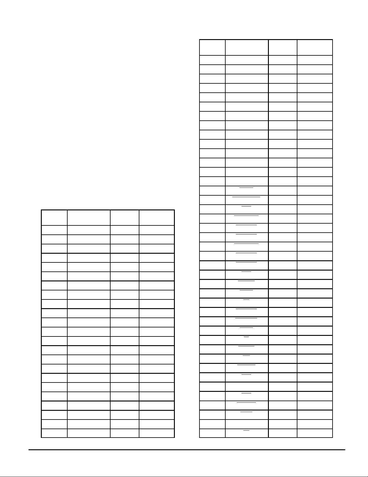
Bit
Number
0 Reserved Reserved
1 DL16 I/O DOE
2 DL17 I/O DOE
3 DL18 I/O DOE
4 DL19 I/O DOE
5 DL20 I/O DOE
6 DL21 I/O DOE
7 DL22 I/O DOE
8 DL23 I/O DOE
9 DP6 I/O DOE
10 DL24 I/O DOE
11 DL25 I/O DOE
12 DL26 I/O DOE
13 DL27 I/O DOE
14 DL28 I/O DOE
15 DL29 I/O DOE
16 DL30 I/O DOE
17 DL31 I/O DOE
18 DP7 I/O DOE
19 DH24 I/O DOE
20 DH25 I/O DOE
21 DH26 I/O DOE
22 DH27 I/O DOE
Bit/Pin Name
Bit/Pin
Type
Output
Enable
Bit
Number
23 DH28 I/O DOE
24 DH29 I/O DOE
25 DH30 I/O DOE
26 DH31 I/O DOE
27 DP3 I/O DOE
28 DH16 I/O DOE
29 DH17 I/O DOE
30 DH18 I/O DOE
31 DH19 I/O DOE
32 DH20 I/O DOE
33 DH21 I/O DOE
34 DH22 I/O DOE
35 DH23 I/O DOE
36 DP2 I/O DOE
37 L2 BG Input
38 L2 MISS INH Input
39 ABB I/O ABBOE
40 CPU3 DBG Input
41 CPU3 BG Input
42 CPU3 BR Input
43 CPU2 DBG Input
44 CPU2 BG Input
45 CPU2 BR Input
46 FDN I/O FDNOE
47 L2 DBG Input
48 L2 BR I/O L2BROE
49 TA I/O TAOE
50 L2 CLAIM Output L2CLAIMOE
51 CPU DBG Input
52 AACK I/O AACKOE
53 CI I/O AOE
54 ARTRY I/O ARTRYOE
55 WT I/O AOE
56 CPU BR Input
57 TEA Input
58 PWRDN Input
59 DBB I/O DBBOE
60 HRESET Input
61 TBST I/O AOE
62 TT0 I/O AOE
63 TS I/O AOE
Bit/Pin Name
Bit/Pin
Type
Output
Enable
MOTOROLA
MPC2605
27
Page 28

Bit
Number
64 TT1 I/O AOE
65 TT2 I/O AOE
66 TT4 I/O AOE
67 TT3 I/O AOE
68 CPU BG Input
69 SRESET Input
70 L2 TAG CLR Input
71 L2 UPDATE INH Input
72 CPU4 BG Input
73 CPU4 DBG Input
74 CPU4 BR Input
75 CFG0 Input
76 CFG2 Input
77 CFG1 Input
79 DH8 I/O DOE
79 DH9 I/O DOE
80 DH10 I/O DOE
81 DH11 I/O DOE
82 DH12 I/O DOE
83 DH13 I/O DOE
84 DH14 I/O DOE
85 DH15 I/O DOE
86 DP1 I/O DOE
87 DH0 I/O DOE
88 DH1 I/O DOE
89 DH2 I/O DOE
90 Dh3 I/O DOE
91 DH4 I/O DOE
92 DH5 I/O DOE
93 DH6 I/O DOE
94 DH7 I/O DOE
95 DP0 I/O DOE
96 DL0 I/O DOE
97 DL1 I/O DOE
98 DL2 I/O DOE
99 DL3 I/O DOE
100 DL4 I/O DOE
101 DL5 I/O DOE
102 DL6 I/O DOE
103 DL7 I/O DOE
104 DP4 I/O DOE
105 DL8 I/O DOE
106 DL9 I/O DOE
Bit/Pin Name
Bit/Pin
Type
Output
Enable
Bit
Number
107 DL10 I/O DOE
108 DL11 I/O DOE
109 DL12 I/O DOE
110 DL13 I/O DOE
111 DL14 I/O DOE
112 DL15 I/O DOE
113 DP5 I/O DOE
114 A0 I/O AOE
115 A1 I/O AOE
116 A2 I/O AOE
117 A3 I/O AOE
118 A4 I/O AOE
119 A5 I/O AOE
120 A6 I/O AOE
121 A7 I/O AOE
122 A8 I/O AOE
123 A9 I/O AOE
124 A10 I/O AOE
125 A11 I/O AOE
126 A12 I/O AOE
127 A31 I/O AOE
128 A30 I/O AOE
129 A29 I/O AOE
130 A28 I/O AOE
131 A27 I/O AOE
132 A26 I/O AOE
133 A25 I/O AOE
134 A24 I/O AOE
135 A23 I/O AOE
136 A22 I/O AOE
137 A21 I/O AOE
138 A20 I/O AOE
139 A19 I/O AOE
140 A18 I/O AOE
141 A17 I/O AOE
142 A16 I/O AOE
143 A15 I/O AOE
144 A14 I/O AOE
145 A13 I/O AOE
146 TSIZ2 I/O AOE
147 TSIZ0 I/O AOE
148 TSIZ1 I/O AOE
149 GBL Output AOE
Bit/Pin Name
Bit/Pin
Type
Output
Enable
MPC2605
28
MOTOROLA
Page 29

Bit
Number
150 CFG3 Input
151 L2 CI Input
152 L2 FLUSH Input
153 AP0 I/O AOE
154 AP1 I/O AOE
155 AP2 I/O AOE
156 AP3 I/O AOE
157 APE Output APEOE
158 TAOE Output
159 L2CLAIMOE Output
160 L2BROE Output
Bit/Pin Name
Bit/Pin
Type
Enable
Enable
Enable
Output
Enable
ORDERING INFORMATION
Bit
Number
161 FDNOE Output
162 DBBOE Output
163 DOE Output
164 ARTRYOE Output
165 APEOE Output
166 ABBOE Output
167 AACKOE Output
168 AOE Output
(Order by Full Part Number)
Bit/Pin Name
Bit/Pin
Type
Enable
Enable
Enable
Enable
Enable
Enable
Enable
Enable
Output
Enable
Motorola PowerPC Prefix
Part Number
MPC 2605 ZP 66 X
Blank = Trays, R = Tape and Reel
Speed (66 = 66 MHz)
Package (ZP = PBGA)
Full Part Number — MPC2605ZP66
MPC2605ZP66R
MOTOROLA
MPC2605
29
Page 30

P ACKAGE DIMENSIONS
ZP PACKAGE
PBGA
CASE 1138–01
0.20
4X
E2
D2
TOP VIEW
D1
W
V
U
T
R
P
N
M
L
K
J
H
G
F
E
D
C
B
A
12345678910111213141516
BOTTOM VIEW
D
A
C
0.20 C
0.25 C
0.35 C
NOTES:
1. DIMENSIONING AND TOLERANCING PER ASME
Y14.5M, 1994.
2. DIMENSIONS IN MILLIMETERS.
3. DIMENSION b IS THE SOLDER BALL DIAMETER
MEASURED PARALLEL TO DATUM C.
MILLIMETERS
DIM MIN MAX
A ––– 2.05
A1 0.50 0.70
A2 0.95 1.35
A3 0.70 0.90
b 0.60 0.90
D 25.00 BSC
D1 22.86 BSC
D2 22.40 22.60
e 1.27 BSC
E 25.00 BSC
E1 22.86 BSC
E2
22.40 22.60
18X
E
B
e
A2
A3
E1
A1
A
SIDE VIEW
241
191817
b
M
0.03 C A B
M
0.15 C
Motorola reserves the right to make changes without further notice to any products herein. Motorola makes no warranty , representation or guarantee regarding
the suitability of its products for any particular purpose, nor does Motorola assume any liability arising out of the application or use of any product or circuit, and
specifically disclaims any and all liability, including without limitation consequential or incidental damages. “T ypical” parameters which may be provided in Motorola
data sheets and/or specifications can and do vary in different applications and actual performance may vary over time. All operating parameters, including “Typicals”
must be validated for each customer application by customer’s technical experts. Motorola does not convey any license under its patent rights nor the rights of
others. Motorola products are not designed, intended, or authorized for use as components in systems intended for surgical implant into the body, or other
applications intended to support or sustain life, or for any other application in which the failure of the Motorola product could create a situation where personal injury
or death may occur. Should Buyer purchase or use Motorola products for any such unintended or unauthorized application, Buyer shall indemnify and hold Motorola
and its officers, employees, subsidiaries, affiliates, and distributors harmless against all claims, costs, damages, and expenses, and reasonable attorney fees
arising out of, directly or indirectly, any claim of personal injury or death associated with such unintended or unauthorized use, even if such claim alleges that
Motorola was negligent regarding the design or manufacture of the part. Motorola and are registered trademarks of Motorola, Inc. Motorola, Inc. is an Equal
Opportunity/Affirmative Action Employer.
How to reach us:
Mfax is a trademark of Motorola, Inc.
USA/EUROPE/Locations Not Listed: Motorola Literature Distribution; JAPAN: Nippon Motorola Ltd.: SPD, Strategic Planning Office, 141,
P.O. Box 5405, Denver, Colorado, 80217 . 1-303-675-2140 or 1-800-441-2447 4-32-1 Nishi-Gotanda, Shagawa-ku, Tokyo, Japan. 03-5487-8488
Mfax: RMFAX0@email.sps.mot.com – TOUCHTONE 1-602-244-6609 ASIA/P ACIFIC: Motorola Semiconductors H.K. Ltd.; 8B Tai Ping Industrial Park,
Motorola Fax Back System – US & Canada ONLY 1-800-774-1848 51 Ting Kok Road, Tai Po, N.T., Hong Kong. 852-26629298
– http://sps.motorola.com/mfax/
HOME PAGE: http://motorola.com/sps/ CUSTOMER FOCUS CENTER: 1-800-521-6274
MPC2605
◊
MPC2605/D
MOTOROLA
30
 Loading...