

Motorola MMBTH81LT1 Datasheet
1
Motorola Small–Signal Transistors, FETs and Diodes Device Data
PNP Silicon
MAXIMUM RATINGS
Rating Symbol Value Unit
Collector–Emitter Voltage V
CEO
–20 Vdc
Collector–Base Voltage V
CBO
–20 Vdc
Emitter–Base Voltage V
EBO
–3.0 Vdc
DEVICE MARKING
MMBTH81LT1 = 3D
THERMAL CHARACTERISTICS
Characteristic Symbol Max Unit
Total Device Dissipation FR-5 Board,
(1)
TA = 25°C
Derate above 25°C
P
D
225
1.8
mW
mW/°C
Thermal Resistance, Junction to Ambient R
θJA
556 °C/W
Total Device Dissipation
Alumina Substrate,
(2)
TA = 25°C
Derate above 25°C
P
D
300
2.4
mW
mW/°C
Thermal Resistance, Junction to Ambient R
θJA
417 °C/W
Junction and Storage Temperature TJ, T
stg
–55 to +150 °C
ELECTRICAL CHARACTERISTICS (T
A
= 25°C unless otherwise noted)
Characteristic
Symbol Min Typ Max Unit
OFF CHARACTERISTICS
Collector–Emitter Breakdown Voltage (IC = –1.0 mAdc, IB = 0) V
(BR)CEO
–20 — — Vdc
Collector–Base Breakdown Voltage (IC = –10 µAdc, IE = 0) V
(BR)CBO
–20 — — Vdc
Emitter–Base Breakdown Voltage (IE = –10 µAdc, IC = 0) V
(BR)EBO
–3.0 — — Vdc
Collector Cutoff Current (VCB = –10 Vdc, IE = 0) I
CBO
— — –100 nAdc
Emitter Cutoff Current (VEB = –2.0 Vdc, IC = 0) I
EBO
— — –100 nAdc
ON CHARACTERISTICS
DC Current Gain (IC = –5.0 mAdc, VCE = –10 Vdc) h
FE
60 — — —
Collector–Emitter Saturation Voltage (IC = –5.0 mAdc, IB = –0.5 mAdc) V
CE(sat)
— — –0.5 Vdc
Base–Emitter On Voltage (IC = –5.0 mAdc, VCE = –10 Vdc) V
BE(on)
— — –0.9 Vdc
SMALL–SIGNAL CHARACTERISTICS
Current–Gain – Bandwidth Product
(IC = –5.0 mAdc, VCE = –10 Vdc, f = 100 MHz)
f
T
600 — — MHz
Collector–Base Capacitance (VCB = –10 Vdc, IE = 0, f = 1.0 MHz) C
cb
— — 0.85 pF
Collector–Emitter Capacitance (IB = 0, VCB = –10 Vdc, f = 1.0 MHz) C
ce
— — 0.65 pF
1. FR–5 = 1.0 x 0.75 x 0.062 in.
2. Alumina = 0.4 x 0.3 x 0.024 in. 99.5% alumina.
Thermal Clad is a trademark of the Bergquist Company
Preferred devices are Motorola recommended choices for future use and best overall value.
Order this document
by MMBTH81LT1/D
SEMICONDUCTOR TECHNICAL DATA
Motorola Preferred Device
1
2
3
CASE 318–08, STYLE 6
SOT–23 (TO–236AB)
Motorola, Inc. 1996
COLLECTOR
3
1
BASE
2
EMITTER
MMBTH81LT1
2
Motorola Small–Signal Transistors, FETs and Diodes Device Data
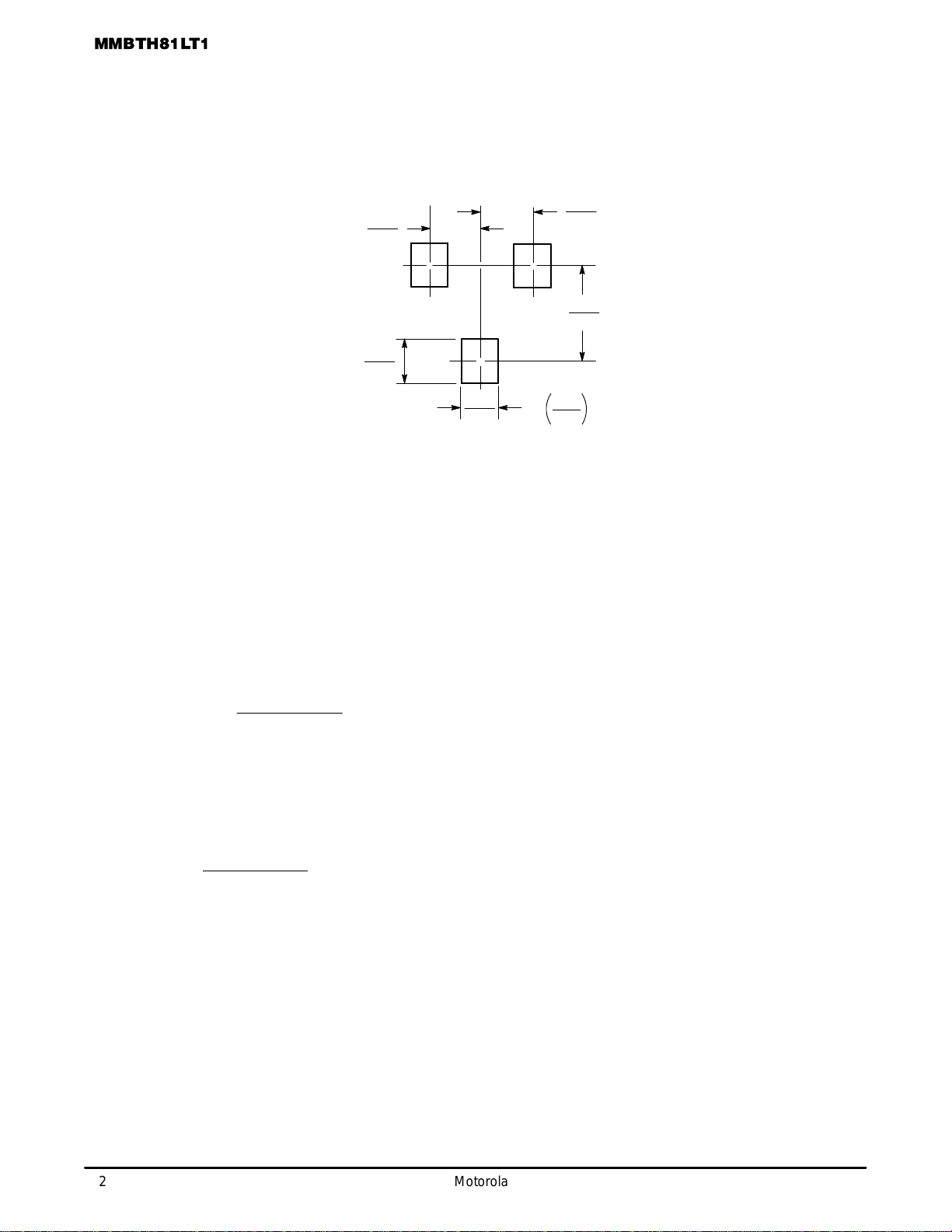
INFORMATION FOR USING THE SOT–23 SURFACE MOUNT PACKAGE
MINIMUM RECOMMENDED FOOTPRINT FOR SURFACE MOUNTED APPLICATIONS
Surface mount board layout is a critical portion of the total
design. The footprint for the semiconductor packages must
be the correct s ize to i nsure proper solder connection
interface between the board and the package. With the
correct pad geometry, the packages will self align when
subjected to a solder reflow process.
SOT–23
mm
inches
0.037
0.95
0.037
0.95
0.079
2.0
0.035
0.9
0.031
0.8
SOT–23 POWER DISSIPATION
The power dissipation of the SOT–23 is a function of the
pad size. This can vary from the minimum p ad size for
soldering to a pad size given for maximum power dissipation.
Power dissipation for a surface mount device is determined
by T
J(max)
, the maximum rated junction temperature of the
die, R
θJA
, the thermal resistance from the device junction to
ambient, and the o perating temperature, TA. Using t he
values provided on the data sheet for the SOT–23 package,
PD can be calculated as follows:
The values for the equation are found in the maximum
ratings table on the data sheet. Substituting these values into
the equation for an ambient temperature TA of 25°C, one can
calculate the power dissipation of the device which in this
case is 225 milliwatts.
The 556°C/W for the SOT–23 package assumes the use
of the recommended footprint on a glass epoxy printed circuit
board to achieve a power dissipation of 225 milliwatts. There
are other alternatives to achieving higher power dissipation
from the SOT–23 package. Another alternative would be to
use a ceramic substrate or an aluminum core board such as
Thermal Clad. Using a board material such as Thermal
Clad, an aluminum core board, the power dissipation can be
doubled using the same footprint.
SOLDERING PRECAUTIONS
The melting temperature of solder is higher than the rated
temperature of the device. When the entire device is heated
to a high temperature, failure to complete soldering within a
short time could result i n device failure. Therefore, t he
following items s hould always be observed in o rder to
minimize the thermal s tress to w hich t he devices a re
subjected.
• Always preheat the device.
• The delta temperature between the preheat and
soldering should be 100°C or less.*
• When preheating and soldering, the temperature of the
leads and the case must not exceed the maximum
temperature ratings as shown on the data sheet. When
using infrared heating with the reflow soldering method,
the difference shall be a maximum of 10°C.
• The soldering temperature and time shall not exceed
260°C for more than 10 seconds.
• When shifting from preheating to soldering, the
maximum temperature gradient shall be 5°C or less.
• After soldering has been completed, the device should
be allowed to cool naturally for at least three minutes.
Gradual cooling should be used as the use of forced
cooling will increase the temperature gradient and result
in latent failure due to mechanical stress.
• Mechanical stress or shock should not be applied during
cooling.
* Soldering a device without preheating can cause excessive
thermal shock and stress which can result in damage to the
device.
PD =
T
PD =
150°C – 25°C
556°C/W
J(max)
R
θJA
– T
A
= 225 milliwatts
 Loading...