

Motorola MMBTA70LT1 Datasheet

1
Motorola Small–Signal Transistors, FETs and Diodes Device Data
PNP Silicon
MAXIMUM RATINGS
Rating Symbol Value Unit
Collector–Emitter Voltage V
CEO
–40 Vdc
Emitter–Base Voltage V
EBO
–4.0 Vdc
Collector Current — Continuous I
C
–100 mAdc
DEVICE MARKING
MMBTA70LT1 = M2C
THERMAL CHARACTERISTICS
Characteristic Symbol Max Unit
Total Device Dissipation FR-5 Board,
(1)
TA = 25°C
Derate above 25°C
P
D
225
1.8
mW
mW/°C
Thermal Resistance, Junction to Ambient R
θJA
556 °C/W
Total Device Dissipation
Alumina Substrate,
(2)
TA = 25°C
Derate above 25°C
P
D
300
2.4
mW
mW/°C
Thermal Resistance, Junction to Ambient R
θJA
417 °C/W
Junction and Storage Temperature TJ, T
stg
–55 to +150 °C
ELECTRICAL CHARACTERISTICS (T
A
= 25°C unless otherwise noted)
Characteristic
Symbol Min Max Unit
OFF CHARACTERISTICS
Collector–Emitter Breakdown Voltage
(IC = –1.0 mAdc, IB = 0)
V
(BR)CEO
–40 — Vdc
Emitter–Base Breakdown Voltage
(IE = –100 µAdc, IC = 0)
V
(BR)EBO
–4.0 — Vdc
Collector Cutoff Current
(VCB = –30 Vdc, IE = 0)
I
CBO
— –100 nAdc
ON CHARACTERISTICS
DC Current Gain
(IC = –5.0 mAdc, VCE = –10 Vdc)
h
FE
40 400 —
Collector–Emitter Saturation Voltage
(IC = –10 mAdc, IB = –1.0 mAdc)
V
CE(sat)
— –0.25 Vdc
SMALL–SIGNAL CHARACTERISTICS
Current–Gain – Bandwidth Product
(IC = –5.0 mAdc, VCE = –10 Vdc, f = 100 MHz)
f
T
125 — MHz
Output Capacitance (VCB = –10 Vdc, IE = 0, f = 1.0 MHz) C
obo
— 4.0 pF
1. FR–5 = 1.0 x 0.75 x 0.062 in.
2. Alumina = 0.4 x 0.3 x 0.024 in. 99.5% alumina.
Thermal Clad is a trademark of the Bergquist Company
Order this document
by MMBTA70LT1/D
SEMICONDUCTOR TECHNICAL DATA
1
2
3
CASE 318–08, STYLE 6
SOT–23 (TO–236AB)
Motorola, Inc. 1996
COLLECTOR
3
1
BASE
2
EMITTER
MMBTA70LT1
2
Motorola Small–Signal Transistors, FETs and Diodes Device Data
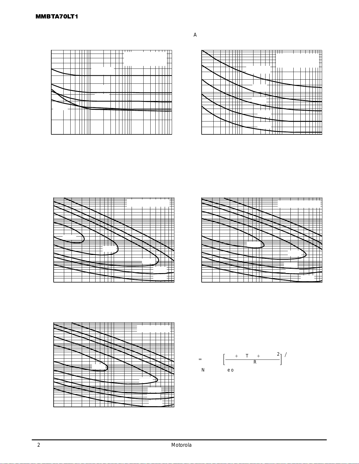
TYPICAL NOISE CHARACTERISTICS
(VCE = –ā5.0 Vdc, TA = 25°C)
Figure 1. Noise Voltage
f, FREQUENCY (Hz)
5.0
7.0
10
3.0
Figure 2. Noise Current
f, FREQUENCY (Hz)
1.0
10 20 50 100 200 500 1.0 k 2.0 k 5.0 k 10 k
1.0
7.0
5.0
3.0
2.0
1.0
0.7
0.5
0.3
0.1
BANDWIDTH = 1.0 Hz
RS
≈
0
IC = 10 µA
100 µA
e
n
, NOISE VOLTAGE (nV)
I
n
, NOISE CURRENT (pA)
30 µA
BANDWIDTH = 1.0 Hz
RS
≈ ∞
IC = 1.0 mA
300 µA
100 µA
30 µA
10 µA
10 20 50 100 200 500 1.0 k 2.0 k 5.0 k 10 k
2.0
1.0 mA
0.2
300 µA
NOISE FIGURE CONTOURS
(VCE = –ā5.0 Vdc, TA = 25°C)
500 k
100
200
500
1.0 k
10 k
5.0 k
20 k
50 k
100 k
200 k
2.0 k
1.0 M
500 k
100
200
500
1.0 k
10 k
5.0 k
20 k
50 k
100 k
200 k
2.0 k
1.0 M
Figure 3. Narrow Band, 100 Hz
IC, COLLECTOR CURRENT (µA)
Figure 4. Narrow Band, 1.0 kHz
IC, COLLECTOR CURRENT (µA)
10
0.5 dB
BANDWIDTH = 1.0 Hz
R
S
, SOURCE RESISTANCE (OHMS)
R
S
, SOURCE RESISTANCE (OHMS)
Figure 5. Wideband
IC, COLLECTOR CURRENT (µA)
10
10 Hz to 15.7 kHz
R
S
, SOURCE RESISTANCE (OHMS)
Noise Figure is Defined as:
NF+20 log
10
ƪ
e
n
2
)
4KTRS)
I
n
2
R
S
2
4KTR
S
ƫ
1ń2
= Noise Voltage of the T ransistor referred to the input. (Figure 3)
= Noise Current of the Transistor referred to the input. (Figure 4)
= Boltzman’s Constant (1.38 x 10
–23
j/°K)
= Temperature of the Source Resistance (°K)
= Source Resistance (Ohms)
e
n
I
n
K
T
R
S
1.0 dB
2.0 dB
3.0 dB
20 30 50 70 100 200 300 500 700 1.0 k 10 20 30 50 70 100 200 300 500 700 1.0 k
500 k
100
200
500
1.0 k
10 k
5.0 k
20 k
50 k
100 k
200 k
2.0 k
1.0 M
20 30 50 70 100 200 300 500 700 1.0 k
BANDWIDTH = 1.0 Hz
5.0 dB
0.5 dB
1.0 dB
2.0 dB
3.0 dB
5.0 dB
0.5 dB
1.0 dB
2.0 dB
3.0 dB
5.0 dB

MMBTA70LT1
3
Motorola Small–Signal Transistors, FETs and Diodes Device Data
TYPICAL STATIC CHARACTERISTICS
Figure 6. DC Current Gain
IC, COLLECTOR CURRENT (mA)
400
0.003
h , DC CURRENT GAIN
FE
TJ = 125°C
–55°C
25°C
VCE = 1.0 V
VCE = 10 V
Figure 7. Collector Saturation Region
IC, COLLECTOR CURRENT (mA)
1.4
Figure 8. Collector Characteristics
IC, COLLECTOR CURRENT (mA)
V, VOLTAGE (VOLTS)
1.0 2.0 5.0 10 20
50
1.6
100
TJ = 25°C
V
BE(sat)
@ IC/IB = 10
V
CE(sat)
@ IC/IB = 10
V
BE(on)
@ VCE = 1.0 V
*
q
VC
for V
CE(sat)
q
VB
for V
BE
0.1 0.2 0.5
Figure 9. “On” Voltages
IB, BASE CURRENT (mA)
0.4
0.6
0.8
1.0
0.2
0
V
CE
, COLLECTOR–EMITTER VOLTAGE (VOLTS)
0.002
TA = 25°C
IC = 1.0 mA 10 mA 100 mA
Figure 10. Temperature Coefficients
50 mA
VCE, COLLECTOR–EMITTER VOLTAGE (VOLTS)
40
60
80
100
20
0
0
I
C
, COLLECTOR CURRENT (mA)
TA = 25°C
PULSE WIDTH = 300
µ
s
DUTY CYCLE
≤
2.0%
IB = 400 µA
350 µA
300 µA
250 µA
200 µA
*APPLIES for IC/IB ≤ hFE/2
25°C to 125°C
–55°C to 25°C
25°C to 125°C
–55°C to 25°C
40
60
0.005 0.01 0.02 0.03 0.05 0.07 0.1 0.2 0.3 0.5 0.7 1.0
2.0
3.0
5.0 7.0 10 20 30 50 70 100
0.005 0.01 0.02 0.05 0.1 0.2 0.5 1.0 2.0 5.0 10 20 5.0 10 15 20 25 30 35 40
1.2
1.0
0.8
0.6
0.4
0.2
0
2.4
0.8
0
1.6
0.8
1.0 2.0 5.0 10 20
50
100
0.1 0.2 0.5
200
100
80
V
, TEMPERATURE COEFFICIENTS (mV/ C)
°θ
150 µA
100 µA
50 µA
 Loading...