

Page 1
MOTOROLA
SUNSTAR传感与控制 http://www.sensor-ic.com/ TEL:0755-83376549 FAX:0755-83376182 E-MAIL:szss20@163.com
SUNSTAR自动化 http://www.sensor-ic.com/ TEL: 0755-83376489 FAX:0755-83376182 E-MAIL:szss20@163.com
SEMICONDUCTOR TECHNICAL DATA
Surface Mount
Micromachined Accelerometer
The MMA series of silicon capacitive, micromachined accelerometers
features signal conditioning, a 4–pole low pass filter and temperature
compensation. Zero–g offset full scale span and filter cut–off are factory set and
require no external devices. A full system self–test capability verifies system
functionality.
Features
• Integral Signal Conditioning
• Linear Output
• Ratiometric Performance
• 4th Order Bessel Filter Preserves Pulse Shape Integrity
• Calibrated Self–test
• Low Voltage Detect, Clock Monitor, and EPROM Parity Check Status
• Transducer Hermetically Sealed at W afer Level for Superior Reliability
• Robust Design, High Shocks Survivability
T ypical Applications
• Vibration Monitoring and Recording
• Appliance Control
• Mechanical Bearing Monitoring
• Computer Hard Drive Protection
• Computer Mouse and Joysticks
• Virtual Reality Input Devices
• Sports Diagnostic Devices and Systems
Order this document
by MMA2201D/D
MMA2201D
MMA2201D: X AXIS SENSITIVITY
MICROMACHINED
ACCELEROMETER
±40g
16
9
1
8
16 LEAD SOIC
CASE 475–01
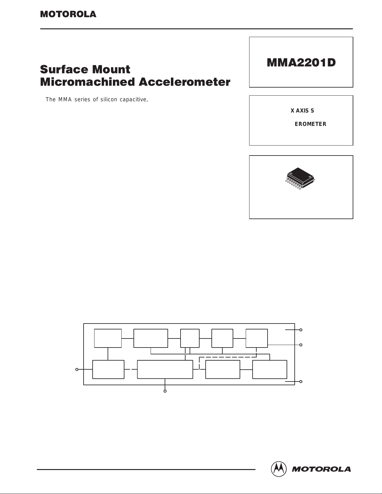
SIMPLIFIED ACCELEROMETER FUNCTIONAL BLOCK DIAGRAM
G–CELL
SENSOR
V
ST
REV 0
Motorola, Inc. 2000
SELF–TEST
Figure 1. Simplified Accelerometer Functional Block Diagram
INTEGRATOR GAIN FILTER
CONTROL LOGIC &
EPROM TRIM CIRCUITS
STATUS
OSCILLATOR
TEMP
COMP
CLOCK GEN.
V
V
V
DD
OUT
SS
1Motorola Sensor Device Data
Page 2
MMA2201D
SUNSTAR传感与控制 http://www.sensor-ic.com/ TEL:0755-83376549 FAX:0755-83376182 E-MAIL:szss20@163.com
SUNSTAR自动化 http://www.sensor-ic.com/ TEL: 0755-83376489 FAX:0755-83376182 E-MAIL:szss20@163.com
MAXIMUM RATINGS
Powered Acceleration (all axes) G
Unpowered Acceleration (all axes) G
Supply Voltage V
Drop Test
Storage Temperature Range T
NOTES:
(1)
1. Dropped onto concrete surface from any axis.
(Maximum ratings are the limits to which the device can be exposed without causing permanent damage.)
Rating Symbol Value Unit
ELECTRO ST ATIC DISCHARGE (ESD)
WARNING: This device is sensitive to electrostatic
discharge.
Although the Motorola accelerometers contain internal
2kV ESD protection circuitry , extra precaution must be taken
by the user to protect the chip from ESD. A charge of over
500 g
2000 g
–0.3 to +7.0 V
1.2 m
–40 to +105 °C
D
pd
upd
DD
drop
stg
2000 volts can accumulate on the human body or associated
test equipment. A charge of this magnitude can alter the performance or cause failure of the chip. When handling the
accelerometer, proper ESD precautions should be followed
to avoid exposing the device to discharges which may be
detrimental to its performance.
2 Motorola Sensor Device Data
Page 3

MMA2201D
SUNSTAR传感与控制 http://www.sensor-ic.com/ TEL:0755-83376549 FAX:0755-83376182 E-MAIL:szss20@163.com
SUNSTAR自动化 http://www.sensor-ic.com/ TEL: 0755-83376489 FAX:0755-83376182 E-MAIL:szss20@163.com
OPERATING CHARACTERISTICS
DD
(1)
5.00
5.0
—
38
2.5
0.50 V
50
10
400
—
—
110
2.0
12
—
—
*
2.0
—
—
0.2
—
—
300
—
10
)
110
DD
5.25
6.0
+85
—
2.7
0.56 V
DD
52.5
10.7
440
+1.0
2.8
—
—
14
0.3 x V
DD
V
DD
*
300
10
0.4
—
—
VDD *0.3
100
—
5.0
—
V
mA
°C
g
V
V
mV/g
mV/g/V
Hz
% FSO
mVrms
µV/(Hz
mVpk
g
V
V
µA
ms
V
V
ms
V
pF
Ω
% FSO
kHz
(Unless otherwise noted: –40°C v TA v +85°C, 4.75 v VDD v 5.25, Acceleration = 0g, Loaded output
Characteristic
Operating Range
Supply Voltage
Supply Current
Operating Temperature Range
Acceleration Range
Output Signal
Zero g (VDD = 5.0 V)
Zero g
Sensitivity (TA = 25°C, VDD = 5.0 V)
Sensitivity
Bandwidth Response
Nonlinearity
Noise
RMS (.01–1 kHz)
Power Spectral Density
Clock Noise (without RC load on output)
Self–Test
Output Response
Input Low
Input High
Input Loading
Response Time
(12)(13)
Status
Output Low (I
Output High (I
Minimum Supply Voltage (LVD Trip) V
Clock Monitor Fail Detection Frequency f
Output Stage Performance
Electrical Saturation Recovery Time
Full Scale Output Range (I
Capacitive Load Drive
Output Impedance
Mechanical Characteristics
Transverse Sensitivity
Package Resonance
NOTES:
1. For a loaded output the measurements are observed after an RC filter consisting of a 1 kΩ resistor and a 0.01 µF capacitor to ground.
2. These limits define the range of operation for which the part will meet specification.
3. Within the supply range of 4.75 and 5.25 volts, the device operates as a fully calibrated linear accelerometer. Beyond these supply limits
the device may operate as a linear device but is not guaranteed to be in calibration.
4. The device can measure both + and * acceleration. With no input acceleration the output is at midsupply. For positive acceleration the output
will increase above VDD/2 and for negative acceleration the output will decrease below VDD/2.
5. The device is calibrated at 20g.
6. At clock frequency ^ 70 kHz.
7. The digital input pin has an internal pull–down current source to prevent inadvertent self test initiation due to external board level leakages.
8. Time for the output to reach 90% of its final value after a self–test is initiated.
9. Time for amplifiers to recover after an acceleration signal causing them to saturate.
10. Preserves phase margin (60°) to guarantee output amplifier stability.
11. A measure of the device’ s ability to reject an acceleration applied 90° from the true axis of sensitivity.
12. The Status pin output is not valid following power–up until at least one rising edge has been applied to the self–test pin. The Status pin is
high whenever the self–test input is high.
13. The Status pin output latches high if a Low Voltage Detection or Clock Frequency failure occurs, or the EPROM parity changes to odd. The
Status pin can be reset by a rising edge on self–test, unless a fault condition continues to exist.
(2)
(3)
(7)
(8)
load
load
(4)
= 100 µA)
= 100 µA)
(10)
(11)
OUT
(5)
(6)
(9)
= 200 µA)
Symbol Min Typ Max Unit
V
DD
I
DD
T
A
g
FS
V
OFF
V
OFF,V
S
S
V
f
–3dB
NL
OUT
n
RMS
n
PSD
n
CLK
g
ST
V
IL
V
IH
I
IN
t
ST
V
OL
V
OH
LVD
min
t
DELAY
V
FSO
C
Z
O
V
ZX,YX
f
PKG
L
4.75
4.0
*
40
—
2.3
0.44 V
DD
47.5
9.3
360
*
1.0
—
—
—
10
V
SS
0.7 x V
*
30
—
—
VDD *.8
2.7 3.25 4.0 V
150 — 400 kHz
—
0.3
—
—
—
—
1/2
)
3Motorola Sensor Device Data
Page 4
MMA2201D
SUNSTAR传感与控制 http://www.sensor-ic.com/ TEL:0755-83376549 FAX:0755-83376182 E-MAIL:szss20@163.com
SUNSTAR自动化 http://www.sensor-ic.com/ TEL: 0755-83376489 FAX:0755-83376182 E-MAIL:szss20@163.com
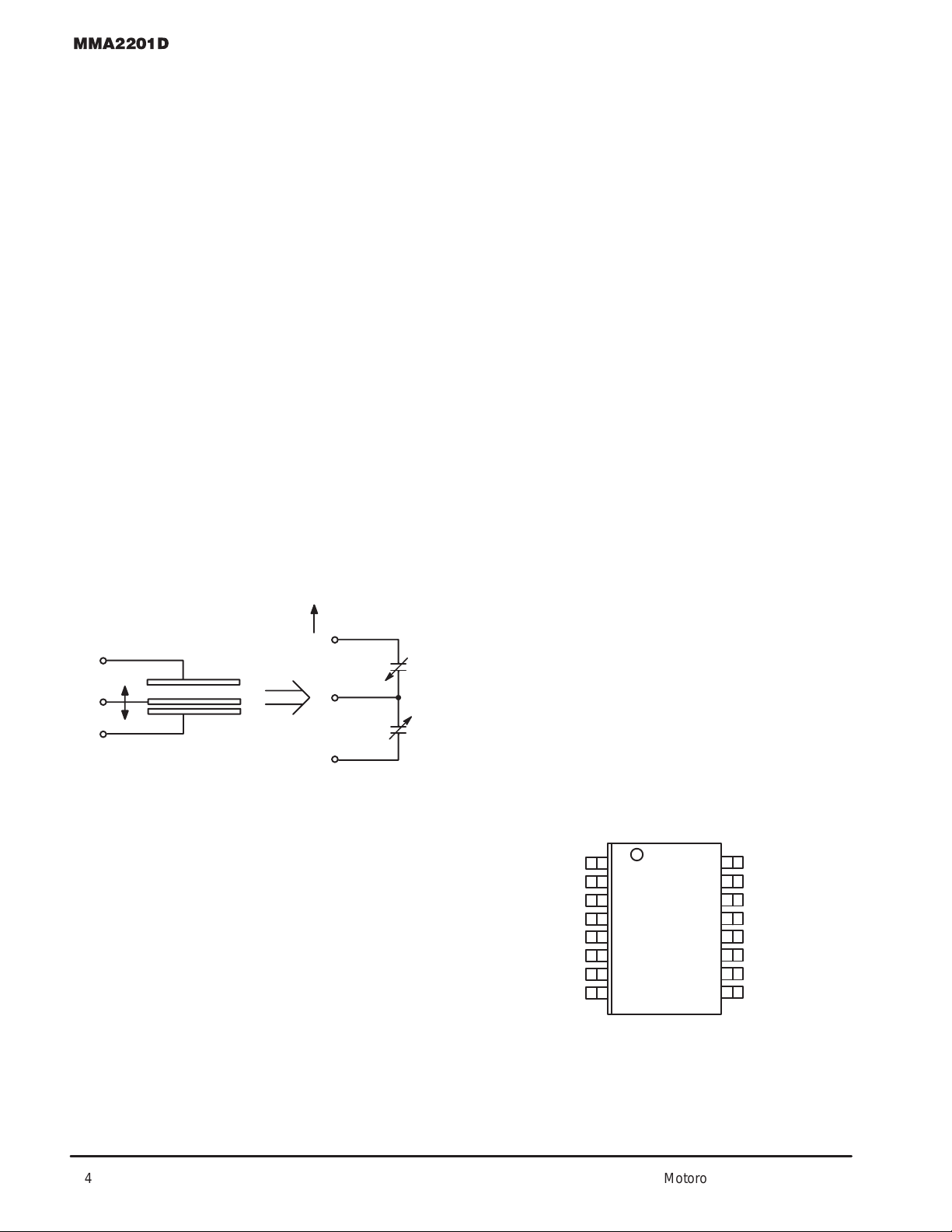
PRINCIPLE OF OPERATION
The Motorola accelerometer is a surface–micromachined
integrated–circuit accelerometer.
The device consists of a surface micromachined capacitive sensing cell (g–cell) and a CMOS signal conditioning
ASIC contained in a single integrated circuit package. The
sensing element is sealed hermetically at the wafer level
using a bulk micromachined “cap’’ wafer .
The g–cell is a mechanical structure formed from semiconductor materials (polysilicon) using semiconductor processes (masking and etching). It can be modeled as two
stationary plates with a moveable plate in–between. The
center plate can be deflected from its rest position by subjecting the system to an acceleration (Figure 2).
When the center plate deflects, the distance from it to one
fixed plate will increase by the same amount that the distance to the other plate decreases. The change in distance is
a measure of acceleration.
The g–cell plates form two back–to–back capacitors
(Figure 3). As the center plate moves with acceleration, the
distance between the plates changes and each capacitor’s
value will change, (C = Aε/D). Where A is the area of the
plate, ε is the dielectric constant, and D is the distance
between the plates.
The CMOS ASIC uses switched capacitor techniques to
measure the g–cell capacitors and extract the acceleration
data from the difference between the two capacitors. The
ASIC also signal conditions and filters (switched capacitor)
the signal, providing a high level output voltage that is ratiometric and proportional to acceleration.
Acceleration
Self–Test
The sensor provides a self–test feature that allows the
verification of the mechanical and electrical integrity of the
accelerometer at any time before or after installation. This
feature is critical in applications such as automotive airbag
systems where system integrity must be ensured over the life
of the vehicle. A fourth “plate’’ is used in the g–cell as a self–
test plate. When the user applies a logic high input to the
self–test pin, a calibrated potential is applied across the
self–test plate and the moveable plate. The resulting electrostatic force (Fe = 1/2 AV2/d2) causes the center plate to
deflect. The resultant deflection is measured by the accelerometer’s control ASIC and a proportional output voltage
results. This procedure assures that both the mechanical
(g–cell) and electronic sections of the accelerometer are
functioning.
Ratiometricity
Ratiometricity simply means that the output offset voltage
and sensitivity will scale linearly with applied supply voltage.
That is, as you increase supply voltage the sensitivity and
offset increase linearly; as supply voltage decreases, offset
and sensitivity decrease linearly. This is a key feature when
interfacing to a microcontroller or an A/D converter because
it provides system level cancellation of supply induced errors
in the analog to digital conversion process.
Status
Motorola accelerometers include fault detection circuitry
and a fault latch. The Status pin is an output from the fault
latch, OR’d with self–test, and is set high whenever one (or
more) of the following events occur:
• Supply voltage falls below the Low Voltage Detect (LVD)
voltage threshold
• Clock oscillator falls below the clock monitor minimum
frequency
• Parity of the EPROM bits becomes odd in number.
The fault latch can be reset by a rising edge on the self–
test input pin, unless one (or more) of the fault conditions
continues to exist.
Figure 2. Transducer
Physical Model
Figure 3. Equivalent
Circuit Model
SPECIAL FEATURES
Filtering
The Motorola accelerometers contain an onboard 4–pole
switched capacitor filter. A Bessel implementation is used
because it provides a maximally flat delay response (linear
phase) thus preserving pulse shape integrity . Because the filter is realized using switched capacitor techniques, there is
no requirement for external passive components (resistors
and capacitors) to set the cut–off frequency.
BASIC CONNECTIONS
Pinout Description
V
N/C
N/C
N/C
ST
OUT
N/C
V
SS
V
DD
1
2
3
4
5
6
7
8
4 Motorola Sensor Device Data
16
15
14
13
12
11
10
N/C
N/C
N/C
N/C
N/C
N/C
N/C
N/C
9
Page 5

Pin No. Pin Name Description
SUNSTAR传感与控制 http://www.sensor-ic.com/ TEL:0755-83376549 FAX:0755-83376182 E-MAIL:szss20@163.com
SUNSTAR自动化 http://www.sensor-ic.com/ TEL: 0755-83376489 FAX:0755-83376182 E-MAIL:szss20@163.com
MMA2201D
PCB Layout
1 thru 3 — No internal connection. Leave
4 ST Logic input pin used to initiate
5 V
6 — No internal connection. Leave
7 V
8 V
9 thru 13 Trim pins Used for factory trim. Leave
14 thru 16 — No internal connection. Leave
V
DD
LOGIC
INPUT
C1
0.1 µF
OUT
SS
DD
4
8
7
ST
V
V
DD
SS
unconnected.
self–test.
Output voltage of the accelerome-
ter.
unconnected.
The power supply ground.
The power supply input.
unconnected.
unconnected.
V
OUT
6
R1
1 kΩ
5
C2
0.01 µF
MMA2201D
STATUS
OUTPUT
SIGNAL
Figure 4. SOIC Accelerometer with Recommended
Connection Diagram
P1STATUS
MICROCONTROLLER
0.1 µF
P0
A/D IN
V
RH
V
SS
C
0.1 µF
V
DD
ST
V
OUT
V
SS
ACCELEROMETER
V
DD
1 kΩ
C
0.1 µF
POWER SUPPLY
R
C
0.01 µF
C
Figure 5. Recommend PCB Layout for Interfacing
Accelerometer to Microcontroller
NOTES:
• Use a 0.1 µF capacitor on VDD to decouple the power
source.
• Physical coupling distance of the accelerometer to the
microcontroller should be minimal.
• Place a ground plane beneath the accelerometer to reduce
noise, the ground plane should be attached to all of the
open ended terminals shown in Figure 5.
• Use an RC filter of 1 kΩ and 0.01 µF on the output of the
accelerometer to minimize clock noise (from the switched
capacitor filter circuit).
• PCB layout of power and ground should not couple power
supply noise.
• Accelerometer and microcontroller should not be a high
current path.
• A/D sampling rate and any external power supply switching
frequency should be selected such that they do not interfere with the internal accelerometer sampling frequency.
This will prevent aliasing errors.
5Motorola Sensor Device Data
Page 6
MMA2201D
SUNSTAR传感与控制 http://www.sensor-ic.com/ TEL:0755-83376549 FAX:0755-83376182 E-MAIL:szss20@163.com
SUNSTAR自动化 http://www.sensor-ic.com/ TEL: 0755-83376489 FAX:0755-83376182 E-MAIL:szss20@163.com
Positive Acceleration Sensing Direction
AXIS
ORIENTATION
–X +X
(ACCELERATION
FORCE
VECTOR)
87654321
10 11 12 13 14 15 16
9
* When positioned as shown, the Earth’s gravity will result in a positive 1g output
N/C
N/C
N/C
SELF TEST
X
OUT
N/C
V
SS
V
DD
N/C pins are recommended to be left FLOATING
Direction of Earth’s gravity field.*
1
2
3
4
5
6
7
8
16–Pin SOIC Package
16
15
14
13
12
11
10
N/C
N/C
N/C
N/C
N/C
N/C
N/C
N/C
9
ORDERING INFORMATION
Device Temperature Range Case No. Package
MMA2201D
*
40 to +85°C Case 475–01 SOIC–16
6 Motorola Sensor Device Data
Page 7

P ACKAGE DIMENSIONS
SUNSTAR传感与控制 http://www.sensor-ic.com/ TEL:0755-83376549 FAX:0755-83376182 E-MAIL:szss20@163.com
SUNSTAR自动化 http://www.sensor-ic.com/ TEL: 0755-83376489 FAX:0755-83376182 E-MAIL:szss20@163.com
MMA2201D
–T–
SEATING
PLANE
–A–
16 9
–B–
18
D 16 PL
0.13 (0.005) B
M
M
A
T
C
K
G
P
8 PL
0.13 (0.005) B
M
M
T
R
K
J
F
CASE 475–01
ISSUE A
16 LEAD SOIC
A
X 45
NOTES:
1. DIMENSIONING AND TOLERANCING PER ANSI
Y14.5M, 1982.
2. CONTROLLING DIMENSION: MILLIMETER.
3. DIMENSIONS A AND B DO NOT INCLUDE MOLD
PROTRUSION.
M
M
_
M
4. MAXIMUM MOLD PROTRUSION 0.15 (0.006) PER
SIDE.
5. DIMENSION D DOES NOT INCLUDE DAMBAR
PROTRUSION. ALLOWABLE DAMBAR
PROTRUSION SHALL BE 0.13 (0.005) TOTAL IN
EXCESS OF D DIMENSION AT MAXIMUM
MATERIAL CONDITION.
DIM MIN MAX MIN MAX
A 10.15 10.45 0.400 0.411
B 7.40 7.60 0.292 0.299
C 3.30 3.55 0.130 0.140
D 0.35 0.49 0.014 0.019
F 0.76 1.14 0.030 0.045
G 1.27 BSC 0.050 BSC
J 0.25 0.32 0.010 0.012
K 0.10 0.25 0.004 0.009
M 0 7 0 7
____
P 10.16 10.67 0.400 0.420
R 0.25 0.75 0.010 0.029
INCHESMILLIMETERS
7Motorola Sensor Device Data
Page 8

MMA2201D
SUNSTAR传感与控制 http://www.sensor-ic.com/ TEL:0755-83376549 FAX:0755-83376182 E-MAIL:szss20@163.com
SUNSTAR自动化 http://www.sensor-ic.com/ TEL: 0755-83376489 FAX:0755-83376182 E-MAIL:szss20@163.com
Motorola reserves the right to make changes without further notice to any products herein. Motorola makes no warranty , representation or
guarantee regarding the suitability of its products for any particular purpose, nor does Motorola assume any liability arising out of the
application or use of any product or circuit, and specifically disclaims any and all liability , including without limitation consequential or incidental
damages. “Typical” parameters which may be provided in Motorola data sheets and/or specifications can and do vary in dif ferent applications
and actual performance may vary over time. All operating parameters, including “Typicals” must be validated for each customer application
by customer’s technical experts. Motorola does not convey any license under its patent rights nor the rights of others. Motorola products are
not designed, intended, or authorized for use as components in systems intended for surgical implant into the body, or other applications
intended to support or sustain life, or for any other application in which the failure of the Motorola product could create a situation where
personal injury or death may occur. Should Buyer purchase or use Motorola products for any such unintended or unauthorized application,
Buyer shall indemnify and hold Motorola and its officers, employees, subsidiaries, affiliates, and distributors harmless against all claims, costs,
damages, and expenses, and reasonable attorney fees arising out of, directly or indirectly , any claim of personal injury or death associated
with such unintended or unauthorized use, even if such claim alleges that Motorola was negligent regarding the design or manufacture of the
part. Motorola and are registered trademarks of Motorola, Inc. Motorola, Inc. is an Equal Opportunity/Affirmative Action Employer.
8 Motorola Sensor Device Data
◊
MMA2201D/D
Page 9

美国 MOTOROLA 压力传感器
SUNSTAR传感与控制 http://www.sensor-ic.com/ TEL:0755-83376549 FAX:0755-83376182 E-MAIL:szss20@163.com
SUNSTAR自动化 http://www.sensor-ic.com/ TEL: 0755-83376489 FAX:0755-83376182 E-MAIL:szss20@163.com
美国 MOTOROLA 公司的 MPX 系列硅压力传感器,主要以气压测量为主,适合用于医疗器械,气体压力控制等领域,输出数字信号。其测量方式可分为:
表压(GP)、绝压(A、AP)、差压(D、DP)型。在宽温度范围工作时需外加补偿网络和信号调整电路。具体型号分类而定
名称:MPX2010DP
名称:MPX5700DP MPX5700GP
名称:MPX2100AP
名称:MPX5500DP
名称:MPX5010DP
名称:MPX5100AP
名称:MPX4115AP
名称:MPX5050DP
名称:MPX2200A
名称:MPX2200AP
名称:MPXH6115A6U
名称:MPX4250DP
Page 10

SUNSTAR传感与控制 http://www.sensor-ic.com/ TEL:0755-83376549 FAX:0755-83376182 E-MAIL:szss20@163.com
SUNSTAR自动化 http://www.sensor-ic.com/ TEL: 0755-83376489 FAX:0755-83376182 E-MAIL:szss20@163.com
名称:MPX4115A
名称:MPX2053GP
名称:MPX2202DP
名称:MPXY8300A6U 压力传感器
名称:MPX2102AP
名称:触力型压力传感器 FSG15N1A
名称:硅压力传感器 MPXH6115A
名称:压力传感器 FPM07
名称:MPX5700DP 硅压力传感器
名称:轮胎压力传感器 TP015
名称:MPX53GP 硅压力传感器
名称:轮胎压力传感器 NPP301
Page 11

SUNSTAR传感与控制 http://www.sensor-ic.com/ TEL:0755-83376549 FAX:0755-83376182 E-MAIL:szss20@163.com
SUNSTAR自动化 http://www.sensor-ic.com/ TEL: 0755-83376489 FAX:0755-83376182 E-MAIL:szss20@163.com
名称:Freescale 压力传感器 MPX2010DP
商斯达实业传感器与智能控制分公司专门从事各种进口传感器的营销工作,代理多家欧美知名公司的产品。涉及压力、温度、湿度、电流、液位、
磁阻、霍尔、流量、称重、光纤、倾角、扭矩、气体、光电、位移、触力、红外、速度、加速度等多种产品。广泛应用于航空航天、医疗器械(如
血压计)、工业控制、冶金化工、汽车制造、教育科研等领域。
商斯达实业代理的品牌产品主要有:
压 力:Kulite、ACSI、Honeywell、Entran、Gems、Dwyer、SSI、Smi、Senstronics、Intersema、Motorola、 NAIS、E+H、Fujikura、Dytran、
APM
称重测力:Transcell、HBM、Interface、Thamesside、Philips、Entran
温 湿 度:Honeywell、Dwyer
流 量:Gems、Dwyer、Honeywell、Folwline、WorldMagnetics
液 位:Honeywell、Siccom、Gems、Dwyer、Kulite、SSI
加 速 度:Entran、Silicondesigns、Dytran
压力开关:ACSI、Gems、Dwyer、台湾矽微
航空器材:TexTech 隔音材料、Honeywell 薄膜加热片、DigirayX 射线探伤仪
仪 表:Honeywell、Transcell、东辉、上润、AD、东崎
商斯达实业 除代理上述产品外,还有几条传感器生产线,一条压力传感器组装线,可为用户提供各种用途的、特殊要求的配套产品。同时还和国
内众多同行建立了友好交流的合作关系。商斯达实业地处深圳,信息资源集中,技术力量雄厚,与国内外有着广泛的联系,本着互利互惠、让利
与长期合作者的原则,以成为企业 "理想的战略伙伴" 为已任,深受业界好评。商斯达实业期待着与您开展更友好、更广泛、更深入的合作!
飞思卡尔 > 传感器
Page 12

MMA7260Q 是一款三轴 (XYZ-Axis) 向低重力加速度传感器,提供 1.5g、2g、4g 和 6g 的可选灵敏度。MMA7260Q
SUNSTAR传感与控制 http://www.sensor-ic.com/ TEL:0755-83376549 FAX:0755-83376182 E-MAIL:szss20@163.com
SUNSTAR自动化 http://www.sensor-ic.com/ TEL: 0755-83376489 FAX:0755-83376182 E-MAIL:szss20@163.com
能够用于各种多功能应用,具备感应坠落、倾斜、移动、定位、撞击和震动的功能。它的封装尺寸很小,只需较
小的板卡空间,另外还提供快速启动和休眠模式,这些特性使 MMA7260Q 成为采用电池供电的电子产品的理想之选,
包括 PDA、手机、3D 游戏和数码相机等。 更多
重点汽车应用
轮胎压力监控系统 (中文)
轮胎压力监控系统(TPMS) 在线座谈 (中文)
重点产品
加速度(Low-g)传感器
MMA7260Q 低重力加速度(low-g)传感器 (中文)
MMA6200xxQ 低重力加速度(low-g)传感器 (中文)
集成压力传感器
MPXAZ 或 MPXHZ 封装的集成压力传感器特别适用于汽车应用
MPXA6115A 高温精确集成压力传感器 (中文)
MPXAZ6115A 媒体耐抗的高温精确集成压力传感器 (中文)
MPXH6115A 高温精确集成压力传感器 (中文)
MP3H6115A 高温精确集成压力传感器 (中文)
MPXHZ6115A 媒体耐抗的高温精确集成压力传感器 (中文)
MPXH6250A 集成压力传感器 (中文)
MPXH6300A 压力传感器 (中文)
MPXH6400A 集成压力传感器 (中文)
美国 motorola/freescale 气压传感器
MPX10D MPX10DP MPX10GP MPX10GS MPXV10GC6U MPXV10GC7U MPX12D MPX12DP MPX12GP MPX2010D MPX2010DP MPX2010GP MPXT2010G7U MPX2050D
MPX2050DP MPX2050GP MPX2050GVP MPX2050GS MPX2050GSX MPX2050GVSX MPX2053D MPX2053DP MPX2053GP MPX2100A MPX2100DP MPX2100AP MPX2100AS
MPX2100ASX MPX2102A MPX2102D MPX2102DP MPX2102AP MPX2102GP MPX2102GVP MPX2200A MPX2200D MPX2200DP MPX2200AP MPX2200GP MPX2200A
MPX2200D MPX2200DP MP2200AP MPX2200GP MPX21002A MPX2102D MPX2102DP MPX2102AP MPX2102GP MPX2102GVP MPX2200A MPX2200D MPX2200DP
MPX2200AP MPX2200GP MPX2201GP MPX2300DT1 MPX4080D MPX4100A MPXA4100A6U MPX4100AP MPXA4100A6U MPX4100AS MPX4101A MPXA4101AC6U
MPX4105A MPX4115A MPXA4115A6U MPX4115AP MPXA4115AC6U MPX4115AS MPX4200A MPX4200AP MPX4200SA MPX4200ASX MPX4250A MPX4250AP MPX4250A6U
MPXA4250A6T1 MPXA4250AC6U MPXA4250AC6T1 MPX4250D MPX4250GP MPX4250DP MPX5010D MPX5010DP MPX5010GP MPX5010GS MPX5010GSX MPXV5010G6U
MPXV5010G7U MPXV5010GC6U/T1 MPXV5010GC7U MPX5050D MPX5050DP MPX5050GP MPX5100A MPX5100D MPX5100DP MPX5100AP MPX5100GP MPX5100GVP
MPX5100AS MPX5100GS MPX5100GVS MPX5100ASX MPX5100GSX MPX5100GVSX MPX53D MPX53GP MPX5500D MPX5500DP MPX5700D MPX5700A MPX5700DP
MPX5700GP MPX5700AP MPX5700GS MPX5700AS MPX5999D MPXA6115A6U MPXA6115AC6U MPXA6115A MPXA6115A6T1 MPXA6115AC6T1 MPXAZ4100A6U
MPXAZ4100A MPXAZ4100A6T1 MPXAZ4100AC6U MPXAZ4100AC6T1 MPXAZ4115A6U MPXZ4115A MPXAZ4115A6T1 MPXAX4115AC6U MPXAZ4115AC6T1 MPXC2011DT1
MPXM2010D MPXM2010DT1 MPXM2010GS MPXM2010GST1 MPXM2053D MPXM2053DT1 MPXM2053GS MPXM2053GST1 MPXV4006GC6U MPXV4006G6U MPXV4115V6U
MPXV4115V6T1 MPXV4115VC6U MPXV5004GC6U/T1 MPXV5004G6U/T1 MPXV5004GC7U MPXV5004G7U MPXY8010 MPXY8020 MPXY8030 MPXY8040 MMA6200xxQ
低重力加速度(low-g)传感器
MPXA6115A 高温精确集成压力传感器 MPXAZ6115A 耐抗高温压力传感器 MPXH6115A 高温精确集成压力传感器
MP3H6115A 高温精确集成压力传感器 MPXHZ6115A 媒体耐抗的高温精确集成压力传感器 MPXH6250A 集成压力传感器 MPXH6300A 压力传感器
MPXH6400A 集成压力传感器 等汽车用压力传感器
Page 13

详情请致电我公司或上我公司网站查询
SUNSTAR传感与控制 http://www.sensor-ic.com/ TEL:0755-83376549 FAX:0755-83376182 E-MAIL:szss20@163.com
SUNSTAR自动化 http://www.sensor-ic.com/ TEL: 0755-83376489 FAX:0755-83376182 E-MAIL:szss20@163.com
美国 motorola 压力传感器
MPX2010 MPX2100 MPX4080D MPX5050 MPX4105A MPX4200
MPX4250D MPX2050 MPX5999D MPX5100 MPX5010 MPX10
MPX4115A MPX4250A
MPX(毫伏输出)选型指南:(D:差压、A:绝压、P:含包装、MPX7000 系列适合电池供电)
型号 压力范围 KPa
MPX10D/DP 10 20 35 50 3.5 75 查看
MPX50D/DP 50 45 60 90 1.2 200 查看
MPX100D/DP/A/AP 100 45 60 90 0.6 200 查看
MPX200D/DP/A/AP 200 45 60 90 0.3 400 查看
MPX700D/DP 700 45 60 90 0.086 2800 查看
MPX2010D/DP 10 24 25 26 2.5 700 查看
MPX2050D/DP 50 38.5 40 41.5 0.8 200 查看
MPX2100D/DP/A/AP 100 38.5 40 41.5 0.4 400 查看
MPX2200D/DP/A/AP 200 38.5 40 41.5 0.2 400 查看
MPX2700D 700 38.5 40 41.5 0.057 2800 查看
MPX7050D/DP 50 38.5 40 41.5 0.8 200 查看
MPX7100D/DP/A/AP 100 38.5 40 41.5 0.4 400 查看
满量程输出,mV
灵敏度 mV/psi 过压 psi,Max 价格<元> 详细资料
Min. Typ. Max.
MPX7200D/DP/A/AP 200 38.5 40 41.5 0.2 400 查看
MPX(标准输出)选型指南
MPX4100A/AP 15-102 4618 4700 4782 54 400 查看
MPX4250A 20-250 4622 4690 4762 20 400 查看
MPX5010D/DP 10 4275 4500 4725 450 75 查看
MPX5050D/DP 50 4388 4500 4613 90 200 查看
MPX5100D/DP 100 4388 4500 4613 45 400 查看
MPX5100A/AP 15-115 4388 4500 4613 45 400 查看
MPX5500D/DP 500 4388 4500 4613 9.0 3500 查看
MPX5700D/DP 700 4388 4500 4613 6.0 2800 查看
MPX5999D/DP 1000 4388 4500 4613 5.0 2800 查看
Page 14

Freescale
SUNSTAR传感与控制 http://www.sensor-ic.com/ TEL:0755-83376549 FAX:0755-83376182 E-MAIL:szss20@163.com
SUNSTAR自动化 http://www.sensor-ic.com/ TEL: 0755-83376489 FAX:0755-83376182 E-MAIL:szss20@163.com
加速度传感器(low g)
型 号
MMA6260Q
MMA6261Q
MMA6262Q
MMA6263Q
MMA2260D
MMA1260D
MMA1270D
MMA1250D
MMA1220D
MMA6231Q
MMA6233Q
型 号
MMA3201D
Acceleration(g) sensing axis sensitivity(mg/v) Rolloff frequency(hz) vdd(v) zero g output package
1.5/1.5 X-Y 800/800 50 3.3 1.65 16pin QFN
1.5/1.5 X-Y 800/800 300 3.3 1.65 16pin QFN
1.5/1.5 X-Y 800/800 150 3.3 1.65 16pin QFN
1.5/1.5 X-Y 800/800 900 3.3 1.65 16pin QFN
1.5 X 1200 50 5.0 2.5 16pin SOIC
1.5 Z 1200 50 5.0 2.5 16pin SOIC
2.5 Z 750 50 5.0 2.5 16pin SOIC
5.0 Z 400 50 5.0 2.5 16pin SOIC
8.0 Z 250 250 5.0 2.5 16pin SOIC
10/10 X-Y 120/120 300 3.3 1.65 16pin QFN
10/10 X-Y 120/120 900 3.3 1.65 16pin QFN
Freescale
Acceleration(g) sensing axis sensitivity(mg/v) Rolloff frequency(hz) vdd(v) zero g output package
40/40 X-Y 50/50 400 5.0 2.5 20pin SOIC
加速度传感器(Medium g)
MMA2201D
MMA2202D
MMA3222D
MMA3204D
MMA3202D
MMA2204D
MMA1213D
MMA1210D
型 号
MMA1211D
MMA2301D
MMA1212D
MMA2300D
MMA1200D
40 X 50 400 5.0 2.5 16pin SOIC
50 X 40 400 5.0 2.5 16pin SOIC
50/30 X-Y 40/66.67 400 5.0 2.5 20pin SOIC
100/30 X-Y 20/66.67 400 5.0 2.5 20pin SOIC
100/50 X-Y 50/100 400 5.0 2.5 20pin SOIC
100 X 20 400 5.0 2.5 16pin SOIC
50 Z 40 400 5.0 2.5 16pin SOIC
100 Z 20 400 5.0 2.5 16pin SOIC
Freescale
Acceleration(g) sensing axis sensitivity(mg/v) Rolloff frequency(hz) vdd(v) zero g output package
150 Z 13 400 5.0 2.5 16pin SOIC
200 X 10 400 5.0 2.5 16pin SOIC
200 Z 10 400 5.0 2.5 16pin SOIC
250 X 8.0 400 5.0 2.5 16pin SOIC
250 Z 8.0 400 5.0 2.5 16pin SOIC
加速度传感器(High g)
Freescale
集成压力传感器
Page 15

型 号
SUNSTAR传感与控制 http://www.sensor-ic.com/ TEL:0755-83376549 FAX:0755-83376182 E-MAIL:szss20@163.com
SUNSTAR自动化 http://www.sensor-ic.com/ TEL: 0755-83376489 FAX:0755-83376182 E-MAIL:szss20@163.com
最大 压力
psi
最大 压力
kpa
最大 压力
in H2O
最大 压力
cm H2O
最大 压力
mm Hg
过压 (kpa)
量程 电压
vdc
灵敏 mV/Kpa
精度 0~85
(% of VFSS)
典型压力
A D G V
MPX4080
MPX4100
MPX4101
MPXA6115A
MPX4105
MPX4115
MPXH6115A
MPX4200
MPX4250
MPXH6250
MPXV4006
MPXV5004
MPX5010
11.6 80 321 815 600 400 4.3 54 ±3.0 •
15.2 105 422 1070 788 400 4.6 54 ±1.8
14.8 102 410 1040 765 400 4.6 54 ±1.8
16.7 115 462 1150 863 400 4.5 45.9 ±1.5
15.2 105 422 1070 788 400 4.6 51 ±1.8
16.7
16.7
16.7 115 462 1150 863 400 4.6 45.9 ±1.5
29 200 803 2040 1500 400 4.5 26 ±1.5
36
36
36 250 1000 2550 1880 400 4.7 19 ±1.5
0.87 6.0 24 61 45 10 4.6 766 ±5.0
0.57 4.0 16 40 29 10 3.9 1000 ±2.5
1.45 10 40 102 75 75 4.5 450 ±5.0
115
115
250
250
462
462
1000
1000
1174
1174
2550
2550
863
863
1880
1880
400
400
400
400
4.6
4.0
4.7
4.7
46
38
20
19
±1.5
±1.5
±1.5
±1.4
•
•
•
•
•
•
•
•
• •
•
• •
• •
• •
•
MPX5050
MPX5100
MPX5500
MPX5700
MPX5999
MPXh6300
MPXH6400
型 号
MPX2010
MPX2053
MPX2102
7.25 50 201 510 375 200 4.5 90 ±2.5
14.5
16.7
72.5 500 2000 5100 3750 2000 4.5 9.0 ±2.5
102 700 2810 7140 5250 2800 4.5 6.0 ±2.5
150 1000 4150 10546 7757 4000 4.5 5.0 ±2.5
44 300 1200 3060 2250 400 4.7 16 ±1.8
60 400 1600 4000 3000 500 4.7 12 ±1.5
最大压力
psi
1.45 10 40 102 75 75 ±1.0 25 2.5 -1.0 1.0 • •
7.0 50 201 510 375 200 ±1.0 40 0.8 -0.6 0.4
14.5
14.5
100
115
最大压力
kpa
100
100
401
462
最大压力
in H2O
400
400
1020
1174
最大压力
cm H2O
1020
750
863
Freescale
最大压力
mm Hg
750
750
400
400
4.5
4.5
带补偿压力传感器
过压
(kpa)
200 200
零位
偏差
mv
±2.0 ±
1.0
量程电压
mv
40
40
灵敏
mV/Kpa
0.4
0.4
45
45
线性%量程
最小
-1.0
-0.6
±2.5
±2.5
• • •
• • •
• •
• • •
•
•
•
线性%量程
最大
A D G V
• •
•
•
1.0
0.4
典型压力
•
Page 16

MPX2202
SUNSTAR传感与控制 http://www.sensor-ic.com/ TEL:0755-83376549 FAX:0755-83376182 E-MAIL:szss20@163.com
SUNSTAR自动化 http://www.sensor-ic.com/ TEL: 0755-83376489 FAX:0755-83376182 E-MAIL:szss20@163.com
29
29
200
200
800
800
2040
1500
1500
400 400
±1.0 ±
1.0
40
40
0.2
0.2
-1.0
-0.6
1.0
0.4
•
•
•
MPX2050
MPX2100
MPX2200
型号
MPX10
MPX12
MPX53
7.0 50 201 510 375 200 ±1.0 40 0.8 -0.3 -0.3
最大
压力
1020
2040
过压
(kpa)
750
750
1500
1500
Freescale
零位
量程
偏差
电压
mv
mv
Freescale
200 200
400 400
±2.0 ±
1.0
±1.0 ±
1.0
40
40
40
40
无补偿压力传感器
线性 %
小
线性 %
量程 最
大
灵敏
mV/Kpa
量程 最
胎压监测传感器
0.4
0.4
0.2
0.2
-1.0
-0.3
-1.0
-0.3
A D G V
-1.0
-0.3
-1.0
-0.3
典型压力
• •
• •
14.5
14.5
29
29
最大
压力
psi
1.45 10 40 102 75 75 20 35 3.5 -1.0 1.0 • •
1.45 10 40 102 75 75 20 55 3.5 -1.0 1.0
7.0 50 200 510 375 200 20 60 1.2 -0.6 0.4
最大
压力
kpa
100
100
200
200
最大
压力
in h2o
最大
压力
cm h2o
400
400
800
800
mm Hg
• •
• •
• •
•
•
型 号
MPXY8020A
MPXY8021A
MPXY8040A
最大 压
力 psi
130.5 900 9.0 8-BIT 5.0 ±25kpa ±20kpa ±4° C 2.1-3.6
最大 压
力 kpa
92.4 637.5 6.4 8-BIT 2.5 ±15kpa ±7.5kpa ±4° C
92.4 637.5 6.4 8-BIT 2.5 ±20kpa ±7.5kpa ±4° C 2.1-3.6
最大 压
力 BAR
量程 输
出
灵敏
kpa/count
最大压力
精度
-20° C
最大压力
精度
+25 ° C-+70° C
最大温度
精度
+25° C
工作电压 v
2.1-3.6
单位换算
单 位 千 帕 mm Hg millibars inchesH2O PSI
典型压力
A D G V
•
•
•
1 大气压 101.325 760.00 1013.25 406.795 14.696
Page 17

1 千帕 1.00000
SUNSTAR传感与控制 http://www.sensor-ic.com/ TEL:0755-83376549 FAX:0755-83376182 E-MAIL:szss20@163.com
SUNSTAR自动化 http://www.sensor-ic.com/ TEL: 0755-83376489 FAX:0755-83376182 E-MAIL:szss20@163.com
1 mm Hg 0.133322 1.00000 1.33322 0.535257 0.0193368
1 millibar 0.100000 0.750062 1.00000 0.401475 0.0145038
1 inch H2o 0.249081 1.86826 2.49081 1.00000 0.0361
1 PSI 6.89473 51.7148 68.9473 27.6807 1.00000
1 hectoPascal 0.100000 0.75006 1.00000 0.401475 0.0145038
1 cm H2O 0.09806 0.7355 9.8x10*7 0.3937 0.014223
7.50062
10.0000 4.01475 0.145038
压力传感器型号解析(MPXA2XXXAPXT1)
M PX A 2 XXX A P X
无 -UNIBODY
AH- SSOP
M -
标准
品
S-
定制
品
P,X-
测试
品
A/V- SOP
AZ -SMALL OUTLINE MEDIA
RESISTANT PACKAGE
压
C-CHIP
力
HZ-SUPER SMALL OUTLINE
传
MEDIA RESISTANT
感
M-M PAK
器
Y-SUPER SMALL OUTLINE
PACKAGE(TPM)
无-无补偿
2-温度补偿校 正
3-open
4--温度补偿校正信
号
自动校准
5- 温度补偿校正信号
6-高温
7-CMOS
8-胎压检测
最大压力
(kpa)
mpx2300
(mmHg)
A-绝对压
力
G-表压
D-差压
V-真空
C-AXIXL PORT(SMALL
OUTLINE PACKAGE)
P-PORTED
SINGLE PORT
(AP,GP,GVP)
DUAL PORT(DP)
S-STOVEPIPE
PORT(UNIBODY)
SX-AXIAL PORT
(UNIBODY)
NONE-NO LEADFORM
0-OPEN
1-2 (CONSULT FACTORY)
3-5 OPEN
6-7 SOP ONLY
(6=GULL WING/SURFACE MOUNT)
(7= 87 DEGREES/DIP)
T1
NONE-TRAYS
T1-TAPE AND REEL
1 INDICATES PART
ORIENTATION IN TAPE
U-RAIL
Page 18

SUNST AR商斯达实业集团是集研发、生产、工程、销售、代理经销 、技术咨询、信息服务等为一体的高
SUNSTAR传感与控制 http://www.sensor-ic.com/ TEL:0755-83376549 FAX:0755-83376182 E-MAIL:szss20@163.com
SUNSTAR自动化 http://www.sensor-ic.com/ TEL: 0755-83376489 FAX:0755-83376182 E-MAIL:szss20@163.com
科技企业,是专业高科技电子产品生产厂家,是具有 10 多年历史的专业电子元器件供应商,是中国最早和
最大的仓储式连锁规模经营大型综合电子零部件代理分销商之一,是一家专业代理和分銷世界各大品牌IC
芯片和電子元器件的连锁经营綜合性国际公司。在香港、北京、深圳、上海、西安、成都等全国主要电子
市场设有直属分公司和产品展示展销窗口门市部专卖店及代理分销商,已在全国范围内建成强大统一的供
货和代理分销网络。 我们专业代理经销、开发生产电子元器件、集成电路、传感器、微波光电元器件、工
控机/DOC/DOM电子盘、专用电路、单片机开发、MCU/DSP/ARM/FPGA软件硬件、二极管、三极管、模
块等,是您可靠的一站式现货配套供应商、方案提供商、部件功能模块开发配套商。专业以现代信息产业
(计算机、通讯及传感器)三大支柱之一的传感器为主营业务,专业经营各类传感器的代理、销售生产、
网络信息、科技图书资料及配套产品设计、工程开发。我们的专业网站——中国传感器科技信息网(全球
传感器数据库) www.SENSOR-IC.COM 服务于全球高科技生产商及贸易商,
术交流平台。
变送器、执行器、自动控制产品厂商介绍产品到 中国,共同开拓市场。本网站是关于各种传感器-变送器-
仪器仪表及工业自动化大型专业网站,深入到工业控制、系统工程计 测计量、自动化、安防报警、消费电
子等众多领域,把最新的传感器-变送器-仪器仪表买卖信息,最新技术供求,最新采购商,行业动态,发展方
向,最新的技术应用和市场资讯及时的传递给广大科技开发、科学研究、产品设计人员。本网站已成功为
石油、化工、电力、医药、生物、航空、航天、国防、能源、冶金、电子、工业、农业、交通、汽车、矿
山、煤炭、纺织、信息、通信、IT、安防、环保、印刷、科研、气象、仪器仪表等领域从事科学研究、产
品设计、开发、生产制造的科技人员、管理人员 、和采购人员提供满意服务。 我公司专业开发生产、代
理、经销、销售各种传感器、变送器、敏感元器件、开关、执行器、仪器仪表、自动化控制系统: 专门从
事设计、生产、销售各种传感器、变送器、各种测控仪表、热工仪表、现场控制器、计算机控制系统、数
据采集系统、各类环境监控系统、专用控制系统应用软件以及嵌入式系统开发及应用等工作。如热敏电阻、
压敏电阻、温度传感器、温度变送器、湿度传感器、 湿度变送器、气体传感器、 气体变送器、压力传感
器、 压力变送、称重传感器、物(液)位传感器、物(液)位变送器、流量传感器、 流量变送器、电流
(压)传感器、溶氧传感器、霍尔传感器 、图像传感器、超声波传感器、位移传感器、速度传感器、加速
度传感器、扭距传感器、红外传感器、紫外传感器、 火焰传感器、激光传感器、振动传感器、轴角传感器、
光电传感器、接近传感器、干簧管传感器、继电器传感器、微型电泵、磁敏(阻)传感器 、压力开关、接
近开关、光电开关、色标传感器、光纤传感器、齿轮测速传感器、 时间继电器、计数器、计米器、温控仪、
固态继电器、调压模块、电磁铁、电压表、电流表等特殊传感器 。 同时承接传感器应用电路、产品设计
和自动化工程项目。
欢迎各厂商互通有无、交换信息、交换链接、发布寻求代理信息。欢迎国外高科技传感器、
为企业科技产品开发提供技
欢迎索取免费详细资料、设计指南和光盘 ;产品凡多,未能尽录,欢迎来电查询。
更多产品请看本公司产品专用销售网站:
商斯达中国传感器科技信息网:http://www.sensor-ic.com/
商斯达工控安防网:http://www.pc-ps.net/
商斯达电子 元器件网:http://www.sunstare.com/
商斯达微波光电产品网:HTTP://www.rfoe.net/
商斯达消费电子产品网://www.icasic.com/
商斯达军工产品网:http://www.junpinic.com/
商斯达实业科技产品网://www.sunstars.cn/传感器销售热线:
地址:深圳市福田区福华路福庆街鸿图大厦
电话:0755-83607652 83376489 83376549 83370250 83370251 82
传真:0755-83376182 (0)13902971329 MSN: SUNS8888@hotmail.com
邮编:518033 E-mail:szss20@163.com QQ: 195847376
深圳赛格展销部:深圳华强北路赛格电子市场
技术支持: 0755-83394033 13501568376
1602 室
500323
2583 号 电话:0755-83665529
Page 19

SUNSTAR 商斯达实业集团是集研发、生产、工程、销售、代理经销 、技术咨询、信息服务等
SUNSTAR传感与控制 http://www.sensor-ic.com/ TEL:0755-83376549 FAX:0755-83376182 E-MAIL:szss20@163.com
SUNSTAR自动化 http://www.sensor-ic.com/ TEL: 0755-83376489 FAX:0755-83376182 E-MAIL:szss20@163.com
为一体的高科技企业,是专业高科技电子产品生产厂家,是具有 10 多年历史的专业电子元器件
供应商,是中国最早和最大的仓储式连锁规模经营大型综合电子零部件代理分销商之一,是一家
专业代理和分銷世界各大品牌 IC 芯片和電子元器件的连锁经营綜合性国际公司,专业经营进口、
国产名厂名牌电子元件,型号、种类齐全。在香港、北京、深圳、上海、西安、成都等全国主要
电子市场设有直属分公司和产品展示展销窗口门市部专卖店及代理分销商,已在全国范围内建成
强大统一的供货和代理分销网络。 我们专业代理经销、开发生产电子元器件、集成电路、传感
器、微波光电元器件、工控机/DOC/DOM 电子盘、专用电路、单片机开发、MCU/DSP/ARM/FPGA
软件硬件、二极管、三极管、模块等,是您可靠的一站式现货配套供应商、方案提供商、部件功
能模块开发配套商。商斯达实业公司拥有庞大的资料库,有数位毕业于著名高校——有中国电子
工业摇篮之称的西安电子科技大学(西军电)并长期从事国防尖端科技研究的高级工程师为您精
挑细选、量身订做各种高科技电子元器件,并解决各种技术问题。
更多产品请看本公司产品专用销售网站:
商斯达中国传感器科技信息网:http://www.sensor-ic.com/
商斯达工控安防网:http://www.pc-ps.net/
商斯达电子元器件网:http://www.sunstare.com/
商斯达微波光电产品网:HTTP://www.rfoe.net/
商斯达消费电子产品网://www.icasic.com/
商斯达实业科技产品网://www.sunstars.cn/
传感器销售热线:
地址:深圳市福田区福华路福庆街鸿图大厦 1602 室
电话:0755-83370250 83376489 83376549 83607652 83370251 82500323
传真:0755-83376182 (0)13902971329 MSN: SUNS8888@hotmail.com
邮编:518033 E-mail:szss20@163.com QQ: 195847376
深圳赛格展销部:深圳华强北路赛格电子市场 2583 号 电话:0755-83665529 25059422
技术支持: 0755-83394033 13501568376
欢迎索取免费详细资料、设计指南和光盘 ;产品凡多,未能尽录,欢迎来电查询。
北京分公司:北京海淀区知春路 132 号中发电子大厦 3097 号
TEL:010-81159046 82615020 13501189838 FAX:010-62543996
上海分公司:上海市北京东路 668 号上海賽格电子市场 2B35 号
TEL:021-28311762 56703037 13701955389 FAX:021-56703037
西安分公司:西安高新开发区 20 所(中国电子科技集团导航技术研究所)
西安劳动南路 88 号电子商城二楼 D23 号
TEL:029-81022619 13072977981 FAX:029-88789382
 Loading...