

Motorola MHW913 Datasheet
SEMICONDUCTOR TECHNICAL DATA
Order this document
by MHW913/D
Designed specifically for the Pan European digital 8.0 watt, GSM mobile
radio. The MHW913 is capable of wide power range control, operates from a
12.5 volt supply and requires less than 100 mW of RF input power.
• Specified 12.5 V Characteristics
RF Input Power ≤ 100 mW (20 dBm)
RF Output Power = 14 W
Minimum Gain = 21.5 dB
Minimum Efficiency = 35%
• 50 Ω Input/Output Impedance
• Guaranteed Stability and Ruggedness
• Epoxy Glass Substrate Eliminates Possibility of Substrate
Fracture
• Circuit board photomaster available upon request by
contacting RF Tactical Marketing in Phoenix, AZ.
MAXIMUM RATINGS
DC Supply Voltage V
RF Input Power P
RF Output Power P
Storage Temperature T
Operating Case Temperature T
(Flange Temperature = 25°C)
Rating
14 WATT
880–915 MHz
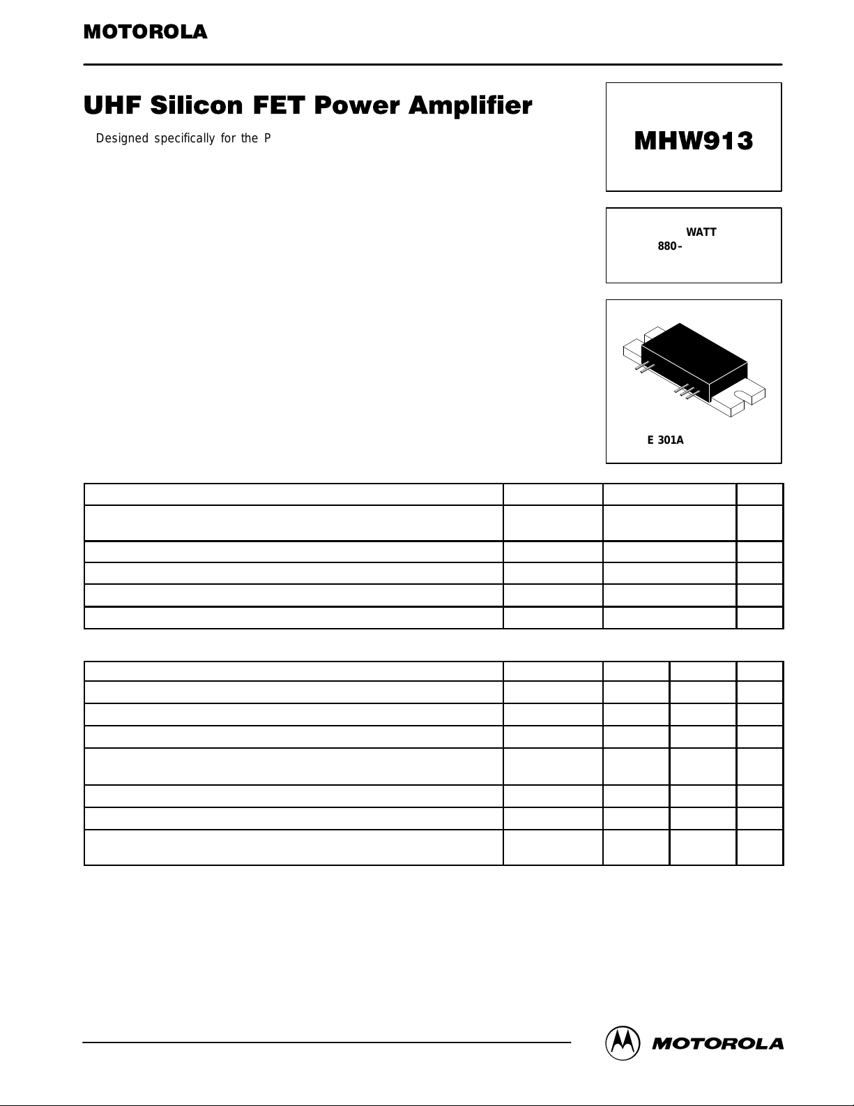
RF POWER AMPLIFIER
CASE 301AB–02, STYLE 1
Symbol Value Unit
bias
VS2, V
out
stg
,
S3
in
C
5.0
15.6
200 mW
15 Watt
– 30 to +100
– 30 to +100
Volt
°C
°C
ELECTRICAL CHARACTERISTICS (V
Characteristic Symbol Min Max Unit
Frequency Range BW 880 915 MHz
Efficiency (P
Power Gain (P
Harmonic Output (P
Input VSWR (P
Linearity — % AM in Output P
Output Power at Decreased Voltage
(Pin = 100 mW, VS2 = VS3 = 10.8 Vdc) (1)
(1) Adjust Pin for specified P
REV 3
= 14 W) (1) η 35 — %
out
= 14 W) (1) G
out
= 14 W Reference) (1) 2f
out
= 14 W) (1) VSWR
out
= 0.02 to 14 W; 135 kHz, 1.0% AM on Input (1) — 6.0 %
out
. (continued)
out
= VS3 = 12.5 Vdc, V
S2
= 4.8 Vdc, TC = 25°C, 50 Ω system, unless otherwise noted)
bias
p
o
3f
o
in
P
out
21.5 — dB
—
—
— 3:1
10 —
–30
–35
dBc
Watt
Motorola, Inc. 1997
MHW913MOTOROLA RF DEVICE DATA
1

ELECTRICAL CHARACTERISTICS (continued) (V
Load Mismatch Stress (V
Load VSWR = 10:1, All Phase Angles) (1)
Stability (V
Load VSWR = 6:1, All Phase Angles) (1)
Quiescent Current (With No RF Applied)
(VS2 = VS3 = 12.5 Vdc, V
Leakage Current (Pin = 0 mW, VS2 = VS3 = 12.5 Vdc, Vb = 0 Vdc) I
Bias Pin Current (P
Noise Power (In 30 kHz Bandwidth, 20 MHz above fo)
(P
= 0.03 to 14 W, VS2 = VS3 = 10.8 to 15.6 Vdc; V
out
(1) Adjust Pin for specified P
= 10.8 to 16 Vdc; P
supply
out
= 14 W) (1) I
supply
bias
out
.
= 15.6 Vdc, P
= 0.03 to 14 W;
out
= 4.8 Vdc)
out
= VS3 = 12.5 V, V
S2
= 15 W;
= 4.8 Vdc) (1)
bias
= 4.8 V, TC = 25°C, 50 Ω system, unless otherwise noted)
bias
MHW913 BLOCK DIAGRAM
— No degradation in
— All spurious outputs more than
I
sq
L
bias
— — –70
output power
60 dB below desired signal
— 500
— 0.6 mA
— 0.8 mA
dBm
OUTPUT
POWER
METER
SPECTRUM
ANALYZER
mA
INPUT
POWER
METER
DIRECTIONAL COUPLER
10 dB
MINIMUM
ATTENUATION
REFLECTED
POWER
METER
20 dB DUAL
RF SIGNAL
GENERATOR
1
Z
RF IN
2345
TEST FIXTURE
C4
C1
1
V
bias
4.8 V
C7
C1, C2, C3 0.018 µF
C4, C5, C6 0.1 µF
C7, C8, C9 1.0 µF
Z1, Z2 50 Ω Microstrip
C5 C6
C8 C3
V
S2
12.5 V
C2
V
S3
12.5 V
C9
Z
2
RF OUT
DIRECTIONAL COUPLER
Figure 1. MHW913 T est Circuit Diagram
20 dB DUAL
POWER
TERMINA TION
MHW913
2
MOTOROLA RF DEVICE DATA
 Loading...