

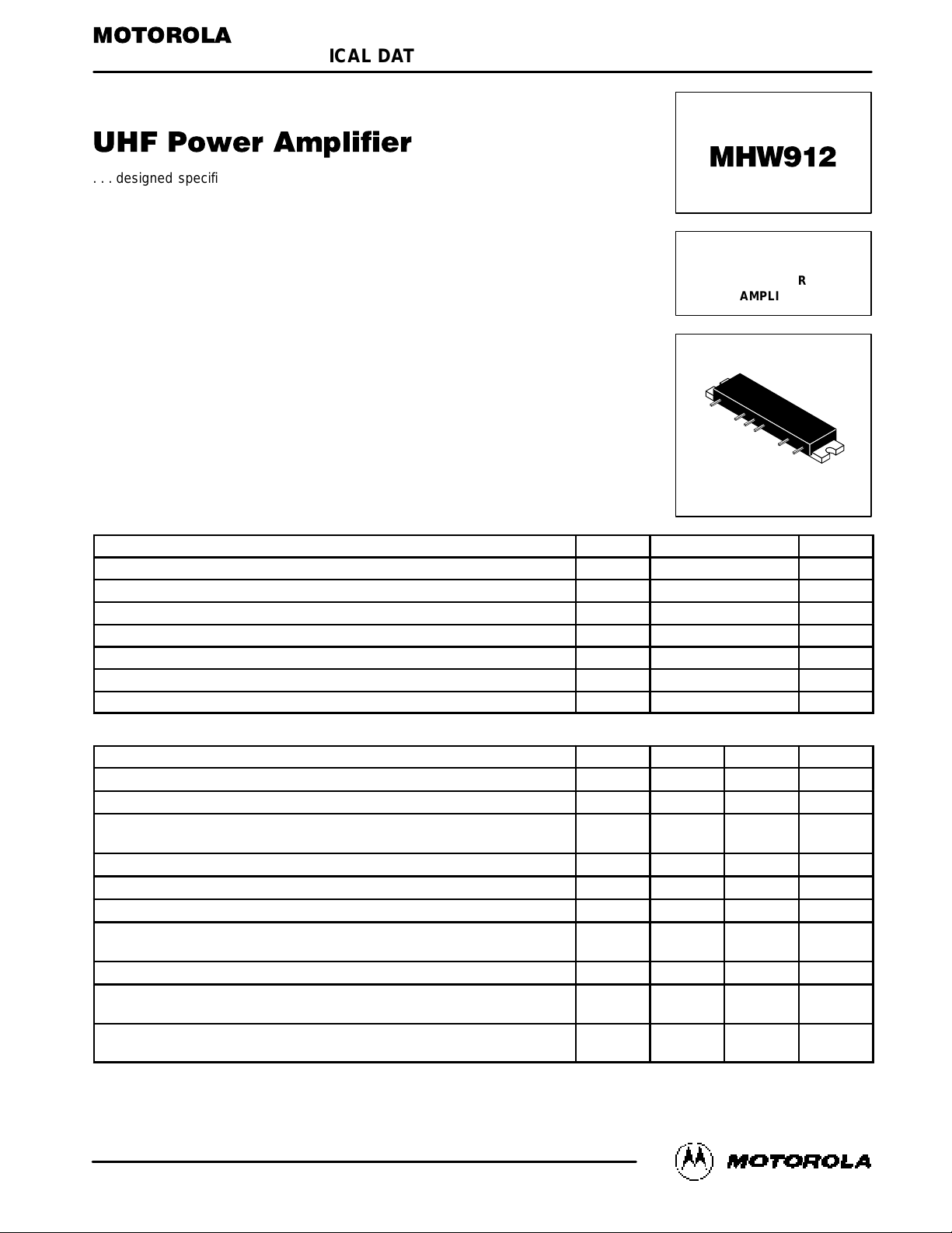
Motorola MHW912 Datasheet
1
MHW912MOTOROLA RF DEVICE DATA
The RF Line
. . . designed specifically for the Pan European digital 8.0 watt, GSM mobile
radio. Other applications exist in standard analog cellular radios. The MHW912
is capable of wide power range control, operates from a 12.5 volt supply and
requires only 1.0 mW of RF input power.
• Specified 12.5 Volt Characteristics:
RF Input Power — 1.0 mW (0 dBm)
RF Output Power — 12.5 W
Minimum Gain — 41 dB
Harmonics — –30 dBc Max @ 2.0 f
o
• New Biasing and Control Techniques Providing Dynamic Range
and Control Circuit Bandwidth Ideal for GSM
• Low Control Current
• 50 Ohm Input/Output Impedances
• Guaranteed Stability and Ruggedness
• Test fixture circuit board photomaster available upon request by contacting
RF Tactical Marketing in Phoenix, AZ.
MAXIMUM RATINGS
(Flange Temperature = 25°C)
Rating
Symbol Value Unit
DC Supply Voltage V
s1, b
8.5 Vdc
DC Supply Voltage — With RF Applied/Without RF Applied V
s2, 3
15.6/30 Vdc
DC Control Voltage V
cont
4.0 Vdc
RF Input Power P
in
3.0 mW
RF Output Power (Vs = 15.6 Vdc) P
out
14 W
Operating Case Temperature Range T
C
– 30 to +100 °C
Storage Temperature Range T
stg
– 30 to +100 °C
ELECTRICAL CHARACTERISTICS (V
s2
= Vs3 = 12.5 Vdc; Vs1 = Vb = 8.0 Vdc; TC = +25°C, 50 ohm system, unless otherwise noted)
Characteristic
Symbol Min Max Unit
Frequency Range BW 884 915 MHz
Output Power (Pin = 1.0 mW; V
cont
= 3.0 Vdc)
P
out
1
12.5 — W
Output Power, Reduced Voltage
(Pin = 1.0 mW; V
cont
= 3.0 Vdc; Vs1 = Vb = 8.0 V; Vs2 = Vs3 = 10.8 Vdc)
P
out
2
8.5 — W
Control Current (P
out
= 12.5 W; Pin = 1.0 mW) (1) I
cont
— 1.0 mA
Current Consumption in 8.0 V Pins (P
out
= 12.5 W; Pin = 1.0 mW) Is1 + I
b
— 220 mA
Leakage Current (Pin = 0 mW; V
cont
= 0; Vs1 = Vb = 0) I
L
— 1.0 mA
Efficiency (P
out
= 12.5 W; Pin = 1.0 mW) (1) f = 890–915 MHz
f = 884–890 MHz
η 35
33
—
—
%
Input VSWR (P
out
= 0.03 to 12.5 W; Pin = 1.0 mW) (1) VSWR
in
— 2.0:1 —
Harmonics (P
out
= 12.5 W; Pin = 1.0 mW) (1) 2 f
o
3 f
o
— —
—
– 30
– 40
dBc
Noise Power (In 30 kHz Bandwidth, 20 MHz Above fo;
P
out
= 12.5 W; Pin = 1.0 mW) (1)
— — – 70 dBm
NOTE:
1. Adjust V
cont
for specified P
out
; Duty Cycle = 12.5%, Period = 4.6 ms.
Order this document
by MHW912/D
SEMICONDUCTOR TECHNICAL DATA
12.5 W
884 to 915 MHz
RF POWER
AMPLIFIER
CASE 301R–01, STYLE 1
Motorola, Inc. 1994
REV 6
MHW912
2
MOTOROLA RF DEVICE DATA
ELECTRICAL CHARACTERISTICS — continued
(Vs2 = Vs3 = 12.5 Vdc; Vs1 = Vb = 8.0 Vdc; TC = +25°C, 50 ohm system, unless otherwise noted)
Characteristic
Symbol Min Max Unit
Isolation
(Pin = 1.0 mW; V
cont
= 0 Vdc; Vs1 = Vb = 0 to 8.0 V)
— — – 36 dBm
3.0 dB V
cont
Bandwidth
(Pin = 1.0 mW; P
out
= 0.03 to 12.5 W) (1)
— 1.0 — MHz
Load Mismatch Stress
(Vs = 15.6 Vdc; Pin = 3.0 mW; P
out
= 14 W; Load VSWR = 10:1,
All Phase Angles at Frequency of Test)(1)
ψ No degradation
in output power
before and after test
Stability
(Vs2 = Vs3 = 10.8 to 15.6 Vdc; Pin = 0.5 to 3.0 mW; P
out
= 12 mW to 12.5 W;
Load VSWR = 6:1, All Phase Angles; Source VSWR = 3:1, All Phase Angles at
Frequency of Test) (1)
—
All spurious outputs
more than 60 dB
below desired signal
NOTE:
1. Adjust V
cont
for specified P
out
; Duty Cycle = 12.5%, Period = 4.6 ms.
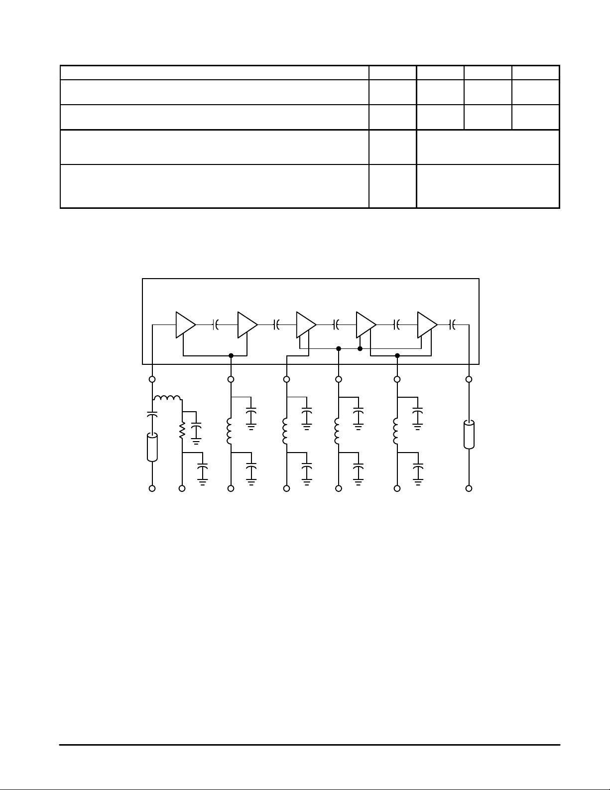
Figure 1. UHF Power Module Test Circuit Diagram
L1
C1
C2
C4
L2 L3 L4 L5
C3 C5
C6
C7
C8
C9
C10
C11
Z2
1 2 3 4 5 6
CIRCUIT BLOCK DIAGRAM
RF INPUT V
cont
V
s1
V
s2
V
s3
V
b
RF OUTPUT
Z1
R
PIN DESIGNATIONS:
PIN 1 — RF INPUT POWER @ 0 dBm AND CONTROL VOLTAGE @ 0–3 Vdc
PIN 2 — FIRST & SECOND STAGE COLLECTOR SUPPLY VOLTAGE @ 8 Vdc
PIN 3 — THIRD STAGE COLLECTOR VOLTAGE @ 12.5 Vdc
PIN 4 — TRICKLE BIAS VOLTAGE @ 8 Vdc
PIN 5 — FOURTH & FIFTH STAGE COLLECTOR SUPPLY VOLTAGE @ 12.5 Vdc
PIN 6 — RF OUTPUT POWER @ 12.5 W
C1 = C2= C4 = C6 = C8 = C10 = 0.018 µF
C3 = C5 = C7 = C9 = C11 = 1 µF
L1–L4 = 0.29 µH
L5 = 0.2 µH
R = 20 OHMS
Z1, Z2 = 50 OHM MICROSTRIP
ELEMENT VALUES:
 Loading...