

Motorola MHW720A1, MHW720A2 Datasheet
1
MHW720A1 MHW720A2MOTOROLA RF DEVICE DATA
The RF Line
Capable o f wide p ower range control as e ncountered i n UHF cellular
telephone applications.
• MHW720A1 400–440 MHz
• MHW720A2 440–470 MHz
• Specified 12.5 Volt, UHF Characteristics —
Output Power = 20 Watts
Minimum Gain = 21 dB
Harmonics = –40 dB (Max)
• 50 Ω Input/Output Impedance
• Guaranteed Stability and Ruggedness
• Epoxy Glass PCB Construction Gives Consistent Performance and Reliability
• Circuit board photomaster available upon request by contacting RF Tactical
Marketing in Phoenix, AZ.
MAXIMUM RATINGS
(Flange Temperature = 25°C)
Rating
Symbol Value Unit
DC Supply Voltages V
s1, Vs2
15.5 Vdc
RF Input Power P
in
250 mW
RF Output Power (@ Vs1 = Vs2 = 12.5 V) P
out
25 W
Operating Case Temperature Range T
C
–30 to +100 °C
Storage Temperature Range MHW720A1, MHW720A2 T
stg
–40 to +100 °C
ELECTRICAL CHARACTERISTICS (V
s1
and Vs2 set at 12.5 Vdc, TC = 25°C, 50 system unless otherwise noted)
Characteristic
Symbol Min Max Unit
Frequency Range MHW720A1
MHW720A2
— 400
440
440
470
MHz
Input Power (P
out
= 20 W) P
in
— 150 mW
Power Gain (P
out
= 20 W) G
p
21 — dB
Efficiency (P
out
= 20 W) MHW720A1, MHW720A2
35 — %
Harmonics (P
out
= 20 W, Reference) — — –40 dB
Input Impedance (P
out
= 20 W, 50 Reference)
Z
in
— 2:1 VSWR
Gain Degradation (1) (P
out
= 20 W, Reference
Gain @ TC = + 25°C) TC = –30°C
TC = +80°C
—
—
—
–0.7
–0.7
dB
Load Mismatch
(VSWR = 30:1, Vs1 = Vs2 = 15.5 Vdc, P
out
= 30 W)
— No degradation
in P
out
Stability (Pin = 0 to 250 mW, Vs1 = Vs2 = 10 to 15.5 Vdc) MHW720A1, MHW720A2
1. Load VSWR = 4:1, 50 Reference
2. Source VSWR = 2:1, 50 Refernece
— All spurious outputs
more than 60 dB
below desired signal
Quiescent Current MHW720A1, MHW720A2
(Is1 No RF Drive Applied)
Is1
(q)
— 200 mA
NOTE:
1. See Figure 5, Input Power versus Case Temperature
Order this document
by MHW720A1/D
SEMICONDUCTOR TECHNICAL DATA
20 W, 400 to 470 MHz
RF POWER
AMPLIFIERS
CASE 700–04, STYLE 2
Motorola, Inc. 1995
REV 7
MHW720A1 MHW720A2
2
MOTOROLA RF DEVICE DATA
APPLICATIONS INFORMATION
Nominal Operation
All electrical specifications a re based on the nominal
conditions of Vs1 (Pin 5) and Vs2 (Pin 3) equal to 12.5 Vdc
and with output power equaling 20 watts. With these conditions, maximum current density on any device is 1.5 x 10
5
A/cm2 and maximum die temperature with 100° base plate
temperature is 165°. While the m odules are d esigned to
have excess gain margin with ruggedness, operation of
these units outside the limits of published specifications is
not recommended unless prior communications regarding intended use has been made with the factory representative.
Gain Control
This module is designed for wide range P
out
level control.
The r ecommended method o f power output control, a s
shown in Figure 3, is to fix Vs1 and Vs2 at 12.5 Vdc and vary
the input RF drive level at Pin 7.
In all applications, the module output power should be lim-
ited to 20 watts.
Decoupling
Due to the high gain of the three stages and the module
size limitation, the e xternal decoupling network r equires
careful consideration. Both Pins 3 and 5 are internally by-
passed with a 0.018 µF chip capacitor effective for frequencies from 5 through 4 70 MHz. For bypassing frequencies
below 5 MHz, networks equivalent to that shown in the test
fixture schematic are recommended. Inadequate decoupling
will result in spurious outputs at certain operating frequencies and certain phase angles of input and output VSWR less
than 4:1.
Load Mismatch
During final test, each module is load mismatch tested in a
fixture having the identical decoupling network described in
Figure 1. Electrical conditions are Vs1 and Vs2 equal 15.5 V ,
load VSWR infinite, and output power equal to 30 watts.
Mounting Considerations
To insure optimum heat transfer from the flange to heatsink, use standard 6–32 mounting screws and an adequate
quantity of silicon thermal compound (e.g., Dow Corning
340). With both mounting s crews finger tight, alternately
torque down the screws to 4–6 inch pounds. The heatsink
mounting surface directly beneath the module flange should
be flat to within 0.005 inch to prevent fracturing of ceramic
substrate material. For more information on module mounting, see EB–107.
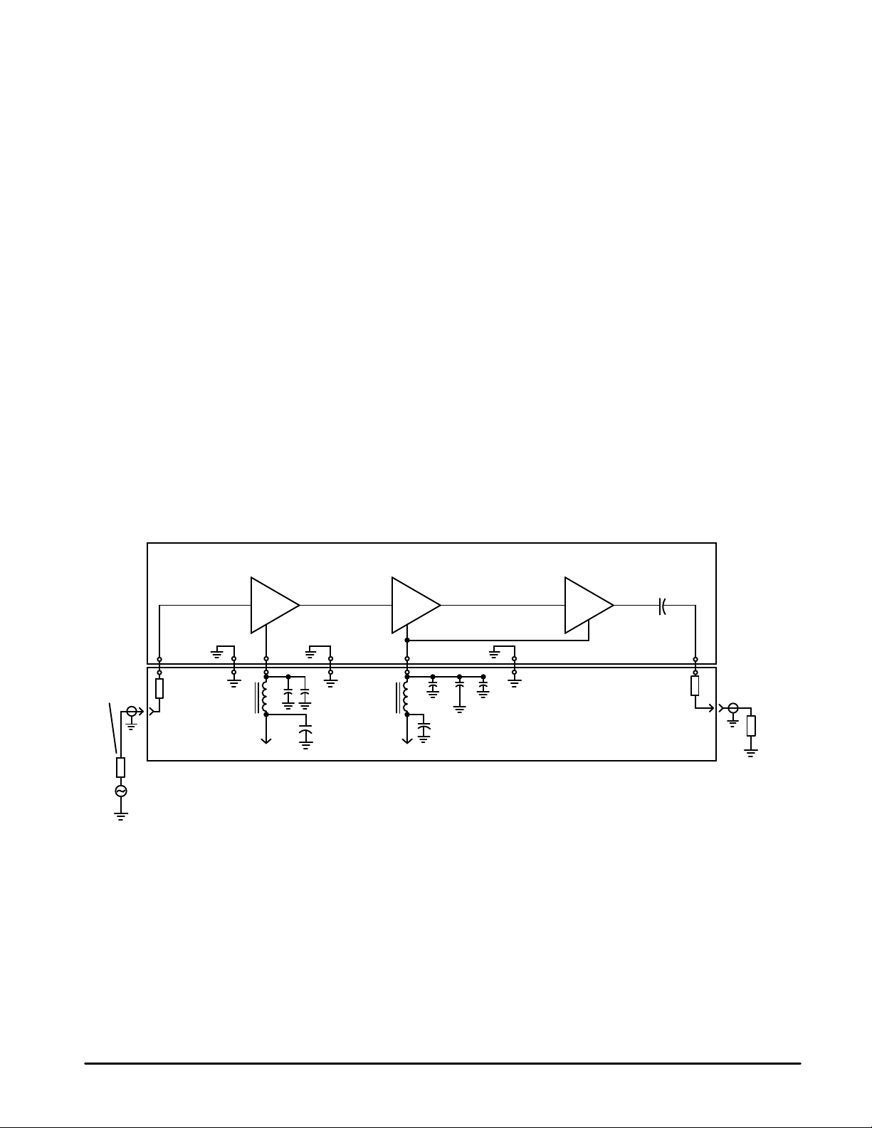
MHW720A BLOCK DIAGRAM
L2
MHW720A Text Fixture Schematic
Z1, Z2 50 Ω Microstripline
L1, L2 Ferroxcube VK200–20/4B
Pin 2
C1, C4, C5, C6 1.0
µ
F Tantalum 25 V
Pin 4
L1
C1 C2
Pin 7
50
Ohm
Load
Z2
Pin 1
C7 47
µ
F Tantalum, 25 V
C2, C3 0.1
µ
F Ceramic
C4
C7
C6
C3
Pin 3
V
s1
V
s2
Pin 5
C5
Pin 6
MICROLAB/ FXR AD 10N
Generator
Signal
10 dB
Z1
NOTE: No Internal D.C. blocking on input pin.
Figure 1. UHF Power Amplifier Test Setup
 Loading...