

SEMICONDUCTOR TECHNICAL DATA
Order this document
by MHPM7A15A60A/D
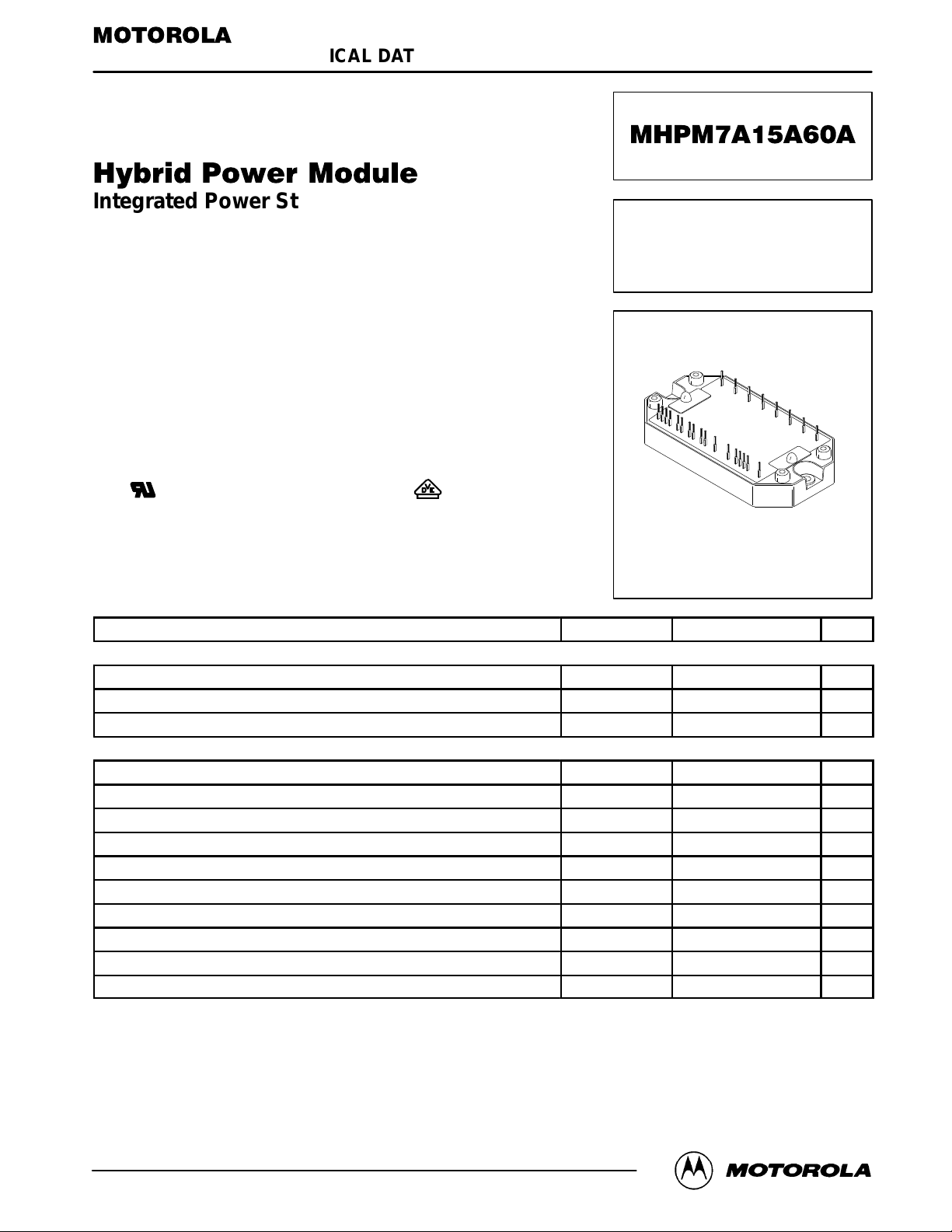
Integrated Power Stage for 1.0 hp Motor Drives
The MHPM7A15A60A module integrates a 3-phase input rectifier bridge,
3-phase output inverter, brake transistor/diode, current sense resistor and
temperature sensor in a single convenient package.The output inverter utilizes
advanced insulated gate bipolar transistors (IGBT) matched with free-wheeling
diodes to give optimal dynamic performance. It has been configured for use as
a three-phase motor drive module or for many other power switching
applications. The top connector pins have been designed for easy interfacing to
the user’s control board.
• DC Bus Current Sense Resistor Included
• Short Circuit Rated 10 µs @ 25°C
• Temperature Sensor Included
• Pin-to-Baseplate Isolation exceeds 2500 V ac (rms)
• Convenient Package Outline
• UL
• Access to Positive and Negative DC Bus
MAXIMUM DEVICE RATINGS (TJ = 25°C unless otherwise noted)
INPUT RECTIFIER BRIDGE
Repetitive Peak Reverse Voltage V
Average Output Rectified Current I
Peak Non-repetitive Surge Current — (1/2 Cycle) (1) I
OUTPUT INVERTER
IGBT Reverse Voltage V
Gate-Emitter Voltage V
Continuous IGBT Collector Current I
Peak IGBT Collector Current — (PW = 1.0 ms) (2) I
Continuous Free-Wheeling Diode Current I
Peak Free-Wheeling Diode Current — (PW = 1.0 ms) (2) I
IGBT Power Dissipation P
Free-Wheeling Diode Power Dissipation P
IGBT Junction Temperature Range T
Free-Wheeling Diode Junction Temperature Range T
(1) 1 cycle = 50 or 60 Hz
(2) 1.0 ms = 1.0% duty cycle
Preferred devices are Motorola recommended choices for future use and best overall value.
Recognized and Designed to Meet VDE
Rating Symbol Value Unit
RRM
O
FSM
CES
GES
C
C(pk)
F
F(pk)
D
D
J
J
Motorola Preferred Device
15 AMP, 600 VOLT
HYBRID POWER MODULE
PLASTIC PACKAGE
CASE 440-01, Style 1
600 V
15 A
200 A
600 V
± 20 V
15 A
30 A
15 A
30 A
55 W
30 W
– 40 to +125 °C
– 40 to +125 °C
Motorola, Inc. 1995
MOTOROLA
MHPM7A15A60A
1

MAXIMUM DEVICE RATINGS (continued) (TJ = 25°C unless otherwise noted)
Rating Symbol Value Unit
BRAKE CIRCUIT
IGBT Reverse Voltage V
Gate-Emitter Voltage V
Continuous IGBT Collector Current I
Peak IGBT Collector Current (PW = 1.0 ms) (2) I
IGBT Power Dissipation PD 55 W
Diode Reverse Voltage V
Continuous Output Diode Current I
Peak Output Diode Current (PW = 1.0 ms) (2) I
TOTAL MODULE
Isolation Voltage — (47–63 Hz, 1.0 Minute Duration) V
Ambient Operating Temperature Range T
Operating Case Temperature Range T
Storage Temperature Range T
Mounting Torque — 6.0 lb–in
CES
GES
C
C(pk)
RRM
F
F(pk)
ISO
A
C
stg
600 V
± 20 V
15 A
30 A
600 V
15 A
30 A
2500 VAC
– 40 to + 85 °C
– 40 to + 90 °C
– 40 to +150 °C
ELECTRICAL CHARACTERISTICS (TJ = 25°C unless otherwise noted)
Characteristic Symbol Min Typ Max Unit
INPUT RECTIFIER BRIDGE
Reverse Leakage Current (V
Forward Voltage (IF = 15 A) V
Thermal Resistance (Each Die) R
OUTPUT INVERTER
Gate-Emitter Leakage Current (VCE = 0 V, VGE = ± 20 V) I
Collector-Emitter Leakage Current (VCE = 600 V, VGE = 0 V)
Gate-Emitter Threshold Voltage (VCE = VGE, IC = 1.0 mA) V
Collector-Emitter Breakdown Voltage (IC = 10 mA, VGE = 0) V
Collector-Emitter Saturation Voltage (VGE = 15 V, IC = 15 A) V
Input Capacitance (VGE = 0 V, VCE = 10 V, f = 1.0 MHz) Cies — 950 — pF
Input Gate Charge (VCE = 300 V, IC = 15 A, VGE = 15 V) Q
Fall Time — Inductive Load
(VCE = 300 V, IC = 15 A, VGE = 15 V, RG = 150 Ω)
Turn-On Energy
(VCE = 300 V, IC = 15 A, VGE = 15 V, RG = 150 Ω)
Turn-Off Energy
(VCE = 300 V, IC = 15 A, VGE = 15 V, RG = 150 Ω)
Diode Forward Voltage (IF = 15 A, VGE = 0 V) V
Diode Reverse Recovery Time
(IF = 15 A, V = 400 V, dI/dt = 50 A/µs)
Diode Stored Charge (IF = 15 A, V = 400 V, di/dt = 50 A/µs) Q
Thermal Resistance — IGBT (Each Die) R
Thermal Resistance — Free-Wheeling Diode (Each Die) R
(2) 1.0 ms = 1.0% duty cycle
= 600 V) I
RRM
TJ = 25°C
TJ = 125°C
R
F
θJC
GES
I
CES
GE(th)
(BR)CES
CE(SAT)
T
t
fi
E
(on)
E
(off)
F
t
rr
rr
θJC
θJC
— 10 50 µA
— 1.05 1.5 V
— — 2.9 °C/W
— — ± 20 µA
—
—
4.0 6.0 8.0 V
600 700 — V
— 2.7 3.5 V
— 75 — nC
— 200 350 ns
— — 1.0 mJ
— — 1.0 mJ
— 1.5 2.0 V
— 140 200 ns
— — 900 nC
— — 1.9 °C/W
— — 3.7 °C/W
—
—
200
2.0
µA
mA
MHPM7A15A60A
2
MOTOROLA

ELECTRICAL CHARACTERISTICS
Characteristic Symbol Min Typ Max Unit
BRAKE CIRCUIT
Gate-Emitter Leakage Current (VCE = 0 V, VGE = ± 20 V) I
Collector-Emitter Leakage Current (VCE = 600 V, VGE = 0 V) (1)
Gate-Emitter Threshold Voltage (VCE = VGE, IC = 1.0 mA) V
Collector-Emitter Breakdown Voltage (IC = 10 mA, VGE = 0) V
Collector-Emitter Saturation Voltage (VGE = 15 V, IC = 15 A) (1) V
Input Capacitance (VGE = 0 V, VCE = 10 V, f = 1.0 MHz) Cies — 950 — pF
Input Gate Charge (VCE = 300 V, IC = 15 A, VGE = 15 V) Q
Fall Time — Inductive Load
(VCE = 300 V, IC = 15 A, VGE = 15 V, RG = 150 Ω)
Turn-On Energy
(VCE = 300 V, IC = 15 A, VGE = 15 V, RG = 150 Ω)
Turn-Off Energy
(VCE = 300 V, IC = 15 A, VGE = 15 V, RG = 150 Ω)
Diode Forward Voltage (IF = 15 A) V
Diode Reverse Leakage Current I
Thermal Resistance — IGBT R
Thermal Resistance — Diode R
SENSE RESISTOR
Resistance R
Resistance Tolerance R
TEMPERATURE SENSE DIODE
Forward Voltage (@ IF = 1.0 mA) V
Forward Voltage Temperature Coefficient (@ IF = 1.0 mA) TC
(1) 1 cycle = 50 or 60 Hz.
(continued) (T
TJ = 25°C
TJ = 125°C
= 25°C unless otherwise noted)
J
GES
I
CES
GE(th)
(BR)CES
CE(SAT)
T
t
fi
E
(on)
E
(off)
F
R
θJC
θJC
sense
tol
F
VF
— — ± 20 µA
—
—
4.0 6.0 8.0 V
600 700 — V
— 2.7 3.5 V
— 75 — nC
— 200 350 ns
— — 1.0 mJ
— — 1.0 mJ
— 1.5 2.0 V
— — 50 µA
— — 1.9 °C/W
— — 3.7 °C/W
— 10 — mΩ
–1.0 — +1.0 %
— 0.660 — V
— –1.95 — mV/°C
—
—
200
2.0
µA
mA
MOTOROLA
MHPM7A15A60A
3

20
U
19
V
18
W
Output
3–Phase
IGBT/Diode
Sense
Bridge,
with Current
and T emperature
Q1 Q3 Q5
D5D1
13
D3
11
9
G5
G3
G1
E5
E3
E1
12
10
8
D6D2
DEVICE INTEGRATION
G6
D4
Q8
TEMP SENSE
C
G4
Q2 Q4 Q6
G2
16 17 14
B
21
–I +IN2N1
+T
3
45625
Brake
3–Phase
C
–T
2
IGBT/
Input
Rectifier
Diode
Bridge
17
P1 P2
Q7
G7
15
S
23
T
22
R
24
Figure 1. Integrated Power Stage Schematic
= PIN NUMBER IDENTIFICATION
MHPM7A15A60A
4
MOTOROLA

V
GE
90%
, FORWARD CURRENT (A)
F
I
50
40
30
20
10
I
C
R
G
L
V
CE
V
CE
t
d(off)
I
C
90%
10%VCE10%
t
f
t
off
Figure 2. Inductive Switching Time Test Circuit and Timing Chart
T ypical Characteristics
25°C125°C
0
VF, FORWARD VOLTAGE (V)
1.20.4 101.0
1.81.40.6 1.00.2
2.01.60.80
1.0
D = 0.5
0.2
0.1
RESISTANCE (NORMALIZED)
r(t), EFFECTIVE TRANSIENT THERMAL
0.01
SINGLE PULSE
P
(pk)
R
= r(t)(R
θ
JC(t)
R
θ
JC
D Curves apply for power pulse
train shown read time at t
T
J(pk)–TC
t, TIME (ms)
= 3.2°C/W
= P
(pk)
θ
JC)
R
θ
t
1
t
1
JC(t)
2
10001000.10.01
Figure 3. Input Bridge Forward Current versus
Forward Voltage
MOTOROLA
Figure 4. Input Rectifier Bridge Thermal
Response
MHPM7A15A60A
5

T ypical Characteristics
, FORWARD CURRENT (A)
F
I
50
40
30
20
10
0
VF, FORWARD VOLTAGE (V)
125°C25°C
Figure 5. Output Inverter Diode Forward Currrent
versus Forward Voltage
20
16
12
8
4
, COLLECTOR-EMITTER VOL TAGE (V)
CE
V
0
5 A
VGE, GATE-EMITTER VOLTAGE (V)
10 A
20 A
50
40
30
20
, COLLECTOR CURRENT (A)
C
10
I
0
542103
20 V
15 V
4
VCE, COLLECTOR–EMITTER VOL TAGE (V)
12 V
10 V
8 V
7 V
8
1060
Figure 6. Output Inverter Collector-Current
versus Collector-Emitter V oltage
450
TJ = 25°C
400
IC = 15 A
350
300
250
200
150
100
, COLLECTOR-EMITTER VOL TAGE (V)V
CE
50
168
201240
0
QG, GATE CHARGE (nC)
100 V
200 V
300 V
18
16
14
12
10
8
, GATE VOLTAGE (V)V
6
GE
4
2
0
1008060402009070503010
Figure 7. Output Inverter Collector-Emitter
V oltage versus Gate-Emitter Voltage
1000
V
= 300 V
CE
VGE = 15 V
RG = 150
µ
100
10
SWITCHING ENERGY ( J)
1
Figure 9. Inverter Switching Energy E
MHPM7A15A60A
6
Ω
125°C
25°C
IC, COLLECTOR CURRENT (A)
Collector Current I
Figure 8. Gate–to–Emitter V oltage versus
Gate Charge
1000
VCE = 300 V
VGE = 15 V
IC = 15 A
µ
100
25°C
SWITCHING ENERGY ( J)
10
100110
RG, GATE RESISTANCE (Ω)
versus
(off)
C
Figure 10. Inverter Switching Energy E
versus Gate Resistance R
G
100010 100
(off)
MOTOROLA

1000
100
VCE = 300 V
VGE = 15 V
RG = 150
Ω
TJ = 25°C
T ypical Characteristics
1000
VCE = 300 V
VGE = 15 V
RG = 150
TJ = 125°C
100
Ω
SWITCHING TIME (ns)
1000
100
SWITCHING TIME (ns)
10
10
1
IC, COLLECTOR CURRENT (A)
Figure 11. Inverter Switching T ime tf, td, t
versus Collector Current I
VCE = 300 V
VGE = 15 V
IC = 15 A
TJ = 25
°
C
RG, GATE RESISTANCE (Ω)
10
t
f
t
d
t
(off)
(off)
C
t
f
t
d
t
(off)
100010 100
SWITCHING TIME (ns)
100101
1
IC, COLLECTOR CURRENT (A)
Figure 12. Inverter Switching Time tf, td, t
versus Collector Current I
1000
V
= 300 V
CE
VGE = 15 V
RG = 150
Ω
125°C
100
SWITCHING TIME (ns)
10
1
25°C
IC, COLLECTOR CURRENT (A)
C
tf @ 125
td @ 125
t
@ 125
(off)
(off)
100110
100110
1000
100
SWITCHING TIME (ns)
10
Figure 13. Inverter Switching Time
VCE = 300 V
VGE = 15 V
IC = 15 A
TJ = 25
1
tf, td, t
°
C
versus Gate Resistance R
(off)
RG, GATE RESISTANCE (Ω)
Figure 15. Inverter Switching Time tr versus
Gate Resistance R
G
Figure 14. Inverter Switching Time tr versus
G
10000
1000
100
CAPACITANCE (pF)
10
100010010
1
Collector Current I
VCE (V)
Figure 16. Inverter Capacitance versus V
C
C
C
C
100
ies
oes
res
1000101
CE
MOTOROLA
MHPM7A15A60A
7

T ypical Characteristics
1.0
D = 0.5
0.2
0.1
RESISTANCE (NORMALIZED)
r(t), EFFECTIVE TRANSIENT THERMAL
0.01
SINGLE PULSE
P
(pk)
R
= r(t)(R
θ
JC(t)
R
θ
JC
D Curves apply for power pulse
train shown read time at t
T
J(pk)–TC
101.0
t, TIME (ms)
= 2.2
°
C/W
= P
θ
(pk)
JC
R
Figure 17. Ouput Inverter IGBT
Thermal Response
40
35
30
25
)
θ
JC(t)
1.0
D = 0.5
0.2
P
= P
θ
(pk)
JC
(pk)
R
)
θ
t
1
JC(t)
t
2
1
10001000.10.01
0.1
t
1
t
2
RESISTANCE (NORMALIZED)
1
10001000.10.01
r(t), EFFECTIVE TRANSIENT THERMAL
0.01
SINGLE PULSE
R
= r(t)(R
θ
JC(t)
R
= 3.4°C/W
θ
JC
D Curves apply for power pulse
train shown read time at t
T
J(pk)–TC
101.0
t, TIME (ms)
Figure 18. Output Diode Thermal Response
, COLLECTOR CURRENT (A)
C
I
20
15
10
L = 200 µH
VGE = 15 V
5
RG = 150
0
Ω
VCE, COLLECTOR-EMITTER VOL TAGE (V)
Figure 19. Output Inverter Reverse Bias Safe
Operating Area (RBSOA)
8006004002000 700500300100
MHPM7A15A60A
8
MOTOROLA

P ACKAGE DIMENSIONS
E
AB
AE AA
AFAC
AD
3 PL
A
AH
2 PL
W
2 PL
N
1
G
L
M
Y
4 PL
25 18
AG
P
U
H
7 PL
J
25 PL
D
F
DETAIL Z
STYLE 1:
PIN 1. P1 PIN 6. N2 PIN 11. G3 PIN 16. G2 PIN 21. B
2. T– 7. P2 12. K5 17. G4 22. T
3. T+ 8. K1 13. G5 18. W 23. S
4. I+ 9. G1 14. G6 19. V 24. R
5. I– 10. K3 15. G7 20. U 25. N1
V
9 PL
C
K
DETAIL Z
Q
2 PL
17
T
B
S
R
NOTES:
1. DIMENSIONING AND TOLERANCING PER ANSI
Y14.5M, 1982.
2. CONTROLLING DIMENSION: MILLIMETER.
X
4 PL
3. LEAD LOCATION DIMENSIONS (ie: M, B. AA...)
ARE TO THE CENTER OF THE LEAD.
DIM MIN MAX MIN MAX
A 97.54 98.55 3.840 3.880
B 52.45 53.47 2.065 2.105
C 14.60 15.88 0.575 0.625
D 0.43 0.84 0.017 0.033
E 10.80 12.06 0.425 0.475
F 0.94 1.35 0.037 0.053
G 1.60 2.21 0.063 0.087
H 8.58 9.19 0.338 0.362
J 0.30 0.71 0.012 0.028
K 18.80 20.57 0.74 0.81
L 19.30 20.32 0.760 0.800
M 38.99 40.26 1.535 1.585
N 9.78 11.05 0.385 0.435
P 82.55 83.57 3.250 3.290
Q 4.01 4.62 0.158 0.182
R 26.42 27.43 1.040 1.080
S 12.06 12.95 0.475 0.515
T 4.32 5.33 0.170 0.210
U 86.36 87.38 3.400 3.440
V 14.22 15.24 0.560 0.600
W 7.62 8.13 0.300 0.320
X 6.55 7.16 0.258 0.282
Y 2.49 3.10 0.098 0.122
AA 2.24 2.84 0.088 0.112
AB 7.32 7.92 0.288 0.312
AC 4.78 5.38 0.188 0.212
AD 8.58 9.19 0.338 0.362
AE 6.05 6.65 0.238 0.262
AF 4.78 5.38 0.188 0.212
AG 69.34 70.36 2.730 2.770
AH ––– 5.08 ––– 0.200
INCHESMILLIMETERS
MOTOROLA
CASE 440-01
ISSUE O
MHPM7A15A60A
9

Motorola reserves the right to make changes without further notice to any products herein. Motorola makes no warranty, representation or guarantee regarding
the suitability of its products for any particular purpose, nor does Motorola assume any liability arising out of the application or use of any product or circuit,
and specifically disclaims any and all liability, including without limitation consequential or incidental damages. “T ypical” parameters can and do vary in different
applications. All operating parameters, including “T ypicals” must be validated for each customer application by customer’s technical experts. Motorola does
not convey any license under its patent rights nor the rights of others. Motorola products are not designed, intended, or authorized for use as components in
systems intended for surgical implant into the body, or other applications intended to support or sustain life, or for any other application in which the failure of
the Motorola product could create a situation where personal injury or death may occur. Should Buyer purchase or use Motorola products for any such
unintended or unauthorized application, Buyer shall indemnify and hold Motorola and its officers, employees, subsidiaries, affiliates, and distributors harmless
against all claims, costs, damages, and expenses, and reasonable attorney fees arising out of, directly or indirectly, any claim of personal injury or death
associated with such unintended or unauthorized use, even if such claim alleges that Motorola was negligent regarding the design or manufacture of the part.
Motorola and are registered trademarks of Motorola, Inc. Motorola, Inc. is an Equal Opportunity/Af firmative Action Employer.
How to reach us:
USA/EUROPE: Motorola Literature Distribution; JAPAN: Nippon Motorola Ltd.; Tatsumi–SPD–JLDC, Toshikatsu Otsuki,
P.O. Box 20912; Phoenix, Arizona 85036. 1–800–441–2447 6F Seibu–Butsuryu–Center, 3–14–2 Tatsumi Koto–Ku, T okyo 135, Japan. 03–3521–8315
MFAX: RMF AX0@email.sps.mot.com – T OUCHTONE (602) 244–6609 HONG KONG: Motorola Semiconductors H.K. Ltd.; 8B Tai Ping Industrial Park,
INTERNET: http://Design–NET.com 51 Ting Kok Road, Tai Po, N.T., Hong Kong. 852–26629298
MHPM7A15A60A
10
2PHX34106L–0 PRINTED IN USA 3/95 IMPERIAL LITHO 12250 4,500 HYBRID POWER MODULE
◊
*MHPM7A15A60A/D*
MHPM7A15A60A/D
MOTOROLA
 Loading...