

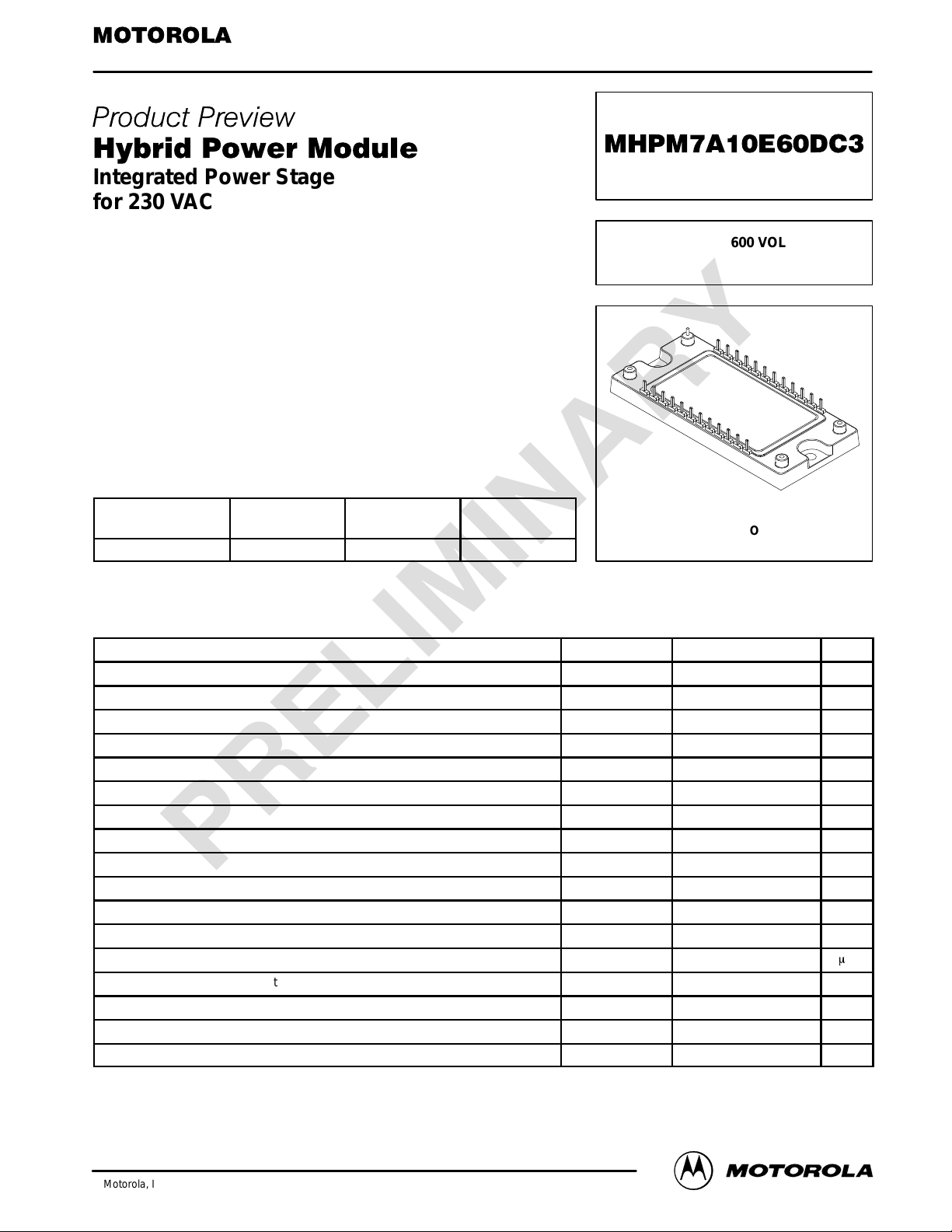
SEMICONDUCTOR TECHNICAL DATA
Integrated Power Stage
for 230 VAC Motor Drive
Order this document
by MHPM7A10E60DC3/D
Motorola Preferred Device
This module integrates a 3–phase inverter, 3–phase rectifier,
brake, and temperature sense in a single convenient package. It is
designed for 1.0 hp general purpose 3–phase induction motor drive
10 AMP, 600 VOLT
HYBRID POWER MODULE
applications. The inverter incorporates advanced insulated gate
bipolar transistors (IGBT) with integrated ESD protection Gate–
Emitter zener diodes and ultrafast soft (UFS) free–wheeling diodes
to give optimum performance. The solderable top connector pins
are designed for easy interfacing to the user’s control board.
• Short Circuit Rated 10 µs @ 125°C, 400 V
• Pin-to-Baseplate Isolation Exceeds 2500 V ac (rms)
• Compact Package Outline
• Access to Positive and Negative DC Bus
• Independent Brake Circuit Connections
• UL Recognition Pending
ORDERING INFORMATION
Voltage
Device
PHPM7A10E60DC3 600 10 1.0
MAXIMUM DEVICE RATINGS (T
Repetitive Peak Input Rectifier Reverse Voltage (TJ = 25°C to 150°C) V
IGBT Reverse Voltage V
Gate-Emitter Voltage V
Continuous IGBT Collector Current (TC = 80°C) I
Repetitive Peak IGBT Collector Current
Continuous Free–Wheeling Diode Current (TC = 25°C) I
Continuous Free–Wheeling Diode Current (TC = 80°C) I
Repetitive Peak Free–Wheeling Diode Current
Average Converter Output Current (Peak–to–Average ratio of 10, TC = 95°C) I
IGBT Power Dissipation per die (TC = 95°C) P
Free–Wheeling Diode Power Dissipation per die (TC = 95°C) P
Junction Temperature Range T
Short Circuit Duration (VCE = 400 V, TJ = 125°C) t
Isolation Voltage, pin to baseplate V
Operating Case Temperature Range T
Storage Temperature Range T
Mounting Torque — Heat Sink Mounting Holes — 12 lb–in
(1) 1.0 ms = 1.0% duty cycle
Preferred devices are Motorola recommended choices for future use and best overall value.
This document contains information on a product under development. Motorola reserves the right to change or discontinue this product without notice.
Rating
= 25°C unless otherwise noted)
J
Rating Symbol Value Unit
(1)
(1)
Current
Rating
Equivalent
Horsepower
RRM
CES
GES
Cmax
I
C(pk)
Fmax
F80
I
F(pk)
Omax
D
D
J
sc
ISO
C
stg
CASE 464D–01
ISSUE O
900 V
600 V
±20 V
10 A
20 A
10 A
6.0 A
20 A
20 A
17 W
9.1 W
–40 to +150 °C
10
2500 Vac
–40 to +95 °C
–40 to +150 °C
m
s
Motorola IGBT Device Data
Motorola, Inc. 1998
1
MHPM7A10E60DC3
ELECTRICAL CHARACTERISTICS
DC AND SMALL SIGNAL CHARACTERISTICS
Input Rectifier Forward Voltage (IF = 10 A) V
Gate–Emitter Leakage Current (VCE = 0 V, VGE = ±20 V) I
Collector–Emitter Leakage Current (VCE = 600 V, VGE = 0 V) I
Gate–Emitter Threshold Voltage (VCE = VGE, IC = 1.0 mA) V
Collector–Emitter Breakdown Voltage (IC = 10 mA, VGE = 0 V) V
Collector–Emitter Saturation Voltage (IC = I
Free–Wheeling Diode Forward Voltage (IF = I
Input Capacitance (VGE = 0 V, VCE = 25 V, f = 1.0 MHz) C
Input Gate Charge (VCE = 300 V, IC = I
THERMAL CHARACTERISTICS, EACH DIE
Thermal Resistance — IGBT
Thermal Resistance — Free–Wheeling (Fast Soft) Diode
Thermal Resistance — Input Rectifier
TEMPERATURE SENSE DIODE
Forward Voltage (@ IF = 1.0 mA) V
Forward Voltage Temperature Coefficient (@ IF = 1.0 mA) TC
(T
= 25°C unless otherwise noted)
J
Characteristic
Cmax
Cmax
Symbol Min Typ Max Unit
(BR)CES
, VGE = 15 V) V
, VGE = 0 V) V
Fmax
, VGE = 15 V) Q
F
GES
CES
GE(th)
CE(sat)
F
ies
T
R
q
JC
R
q
JC
R
q
JC
F
VF
— 0.92 1.1 V
— — ±20
— 5.0 100
4.0 6.0 8.0 V
600 — — V
— 2.0 2.4 V
1.7 2.0 2.3 V
— 1020 — pF
— 57 — nC
— 2.6 3.2 °C/W
— 4.8 6.0 °C/W
— 3.4 4.2 °C/W
1.983 2.024 2.066 V
— –8.64 — mV/°C
m
A
m
A
2
Motorola IGBT Device Data

TYPICAL CHARACTERISTICS
MHPM7A10E60DC3
20
15
10
5.0
, FORWARD CURRENT (AMPS)
F
I
20
15
20
TJ = 125°C
25°C
0
0.2 1.00.8
0.4 0.6
VF, FORWARD VOLTAGE (VOLTS)
1.20
Figure 1. Forward Characteristics —
Input Rectifier
20 V
12.5 V
17.5 V
15 V
VGE = 10 V
18
16
14
12
10
8.0
6.0
, FORWARD CURRENT (AMPS)
4.0
F
I
2.0
0
20
15
TJ = 125°C
0
0.5 1.0 1.5 2.0
VF, FORWARD VOLTAGE (VOLTS)
Figure 2. Forward Characteristics —
Free–Wheeling Diode
20 V
12.5 V
25°C
3.02.5
17.5 V
15 V
VGE = 10 V
10
0.5
, COLLECTOR CURRENT (AMPS)
C
I
0
5.0
4.0
3.0
2.0
1.0
0
–1.0
–2.0
–3.0
, GATE CLAMP DIODE CURRENT (mA)
–4.0
G
I
–5.0
10
0.5
, COLLECTOR CURRENT (AMPS)
C
I
0
VCE, COLLECTOR–TO–EMITTER VOLTAGE (VOLTS)
3.01.0
TJ = 125°C
4.02.0
0
VCE, COLLECTOR–TO–EMITTER VOLTAGE (VOLTS)
3.01.0 2.0 4.0 5.0
TJ = 25°C
Figure 3. Forward Characteristics, TJ = 25°C Figure 4. Forward Characteristics, TJ = 125°C
+15 V
MBRS1100T3
W
20
R
G(off)
120
R
G(on)
W
MBRS1100T3
TJ = 25°C
–20 0–30
–10 10 3020
VGE, GATE–T O–EMITTER VOLTAGE (VOLTS)
MC33153
MBRS1100T3
5.00
Figure 5. Gate–Emitter Zener Diode
Clamp Characteristic
Motorola IGBT Device Data
Figure 6. Recommended Gate Drive Circuit
3

MHPM7A10E60DC3
+15 V
TYPICAL CHARACTERISTICS
2.5
2.0
MAXIMUM
TYPICAL
MINIMUM
Figure 7. Recommended T emperature Sense
MOTOR OUTPUT
U
V
W
R1
12.4 k
14
15
21
W
A/D INPUT
Bias Circuit
1.5
1.0
TYPICAL
VF = 2.240 – 0.00864 T
0.5
, FORWARD VOLTAGE @ 1 mA (VOLTS)
F
V
MIN: 2.199 – 0.00864 T
MAX: 2.282 – 0.00864 T
0
20 40 60 80
100 120
T, TEMPERATURE (°C)
140
1600
Figure 8. BA V99LT1 Temperature Sense Diode
Performance: VF = 2.59 – 7.31E–3 T
BRAKE RESISTOR
43
65
7 8 9 10 12
11
C
R
ST3 PHASE INPUT
D1
D2
R1
SENSE
RESISTOR
Q1
Q2
24
Q3
D3
Q4
D4
23
22
R2 R3
D7
Q5
D5
TEMP
SENSE
D14
Q6
D6
21 20
19
18 17 16 15 14 13
+
C1
Q7
Figure 9. Schematic of Module, Showing Pin–Out and
External Connections
D12D10D8
D13D11D9
FILTER
R NTC
FILTER
4
Motorola IGBT Device Data

0.175
0.175
0.585
0.450
0.250
MHPM7A10E60DC3
KEEP–OUT ZONES (x4)
0.066
1.850
0.925
NOTES:
1. Package is symmetrical, except for a polarizing plastic post near pin 1,
indicated by a non–plated thru–hole in the footprint.
2. Dimension of plated thru–holes indicates finished hole size after plating.
3. Access holes for mounting screws may or may not be necessary depending on
assembly plan for finished product.
0.270
0.140
NON–PLATED
THRU–HOLE
PLATED THRU–HOLES (x24)
Figure 10. Package Footprint (Dimensions in Inches)
OPTIONAL NON–PLATED
THRU–HOLES FOR ACCESS
TO HEAT SINK MOUNTING
SCREWS (x2)
Motorola IGBT Device Data
5

MHPM7A10E60DC3
P ACKAGE DIMENSIONS
AA
M
4 PL
NOTES:
1. DIMENSIONING AND TOLERANCING PER ANSI
Y14.5M, 1982.
2. CONTROLLING DIMENSION: MILLIMETER.
3. LEAD LOCATION DIMENSIONS (ie: P, Q, R, S...)
ARE TO THE CENTER OF THE LEAD.
DIM MIN MAX MIN MAX
A 111.51 112.52 4.390 4.430
B 50.93 51.94 2.005 2.045
C 12.32 13.59 0.485 0.535
D 0.89 1.65
E 8.64 9.65
F 0.13 0.64
G 5.97 6.73
H 46.48 47.50
J 0.41 1.22
K 16.26 17.27
L 3.71 4.72
M 5.46 6.48
N 10.92 11.94
P 37.60 38.60
Q 2.01 2.62
R 23.24 23.75
S 14.35 15.37
U 99.10 100.08
V 81.28 82.55
W 42.67 43.69 1.680 1.720
Y 5.15 5.77 0.203 0.227
X 11.30 12.07 0.445 0.475
AA 2.01 2.72 0.079 0.107
F
AB 16.26 17.27 0.640 0.680
0.035 0.065
0.340 0.380
0.005 0.025
0.235 0.265
1.830 1.870
0.016 0.048
0.640 0.680
0.146 0.186
0.215 0.255
0.430 0.470
1.480 1.520
0.079 0.103
0.915 0.935
0.565 0.605
3.900 3.940
3.200 3.240
DETAIL Z
INCHESMILLIMETERS
A
U
Q3 PL
Y2 PL
23
1
NPB
456
789101112
H
R
24
23 22 21 20 19 18 17 16 15 14 13
S
G 22 PL
J
DETAIL Z
D
24 PL
24 PL
AB
X
C
V
K
E
L
W
CASE 464D–01
ISSUE O
Motorola reserves the right to make changes without further notice to any products herein. Motorola makes no warranty , representation or guarantee regarding
the suitability of its products for any particular purpose, nor does Motorola assume any liability arising out of the application or use of any product or circuit, and
specifically disclaims any and all liability, including without limitation consequential or incidental damages. “T ypical” parameters which may be provided in Motorola
data sheets and/or specifications can and do vary in different applications and actual performance may vary over time. All operating parameters, including “Typicals”
must be validated for each customer application by customer’s technical experts. Motorola does not convey any license under its patent rights nor the rights of
others. Motorola products are not designed, intended, or authorized for use as components in systems intended for surgical implant into the body, or other
applications intended to support or sustain life, or for any other application in which the failure of the Motorola product could create a situation where personal injury
or death may occur. Should Buyer purchase or use Motorola products for any such unintended or unauthorized application, Buyer shall indemnify and hold Motorola
and its officers, employees, subsidiaries, affiliates, and distributors harmless against all claims, costs, damages, and expenses, and reasonable attorney fees
arising out of, directly or indirectly, any claim of personal injury or death associated with such unintended or unauthorized use, even if such claim alleges that
Motorola was negligent regarding the design or manufacture of the part. Motorola and are registered trademarks of Motorola, Inc. Motorola, Inc. is an Equal
Opportunity/Affirmative Action Employer.
How to reach us:
USA/EUROPE/Locations Not Listed: Motorola Literature Distribution; JAPAN: Nippon Motorola Ltd.: SPD, Strategic Planning Office, 141,
P.O. Box 5405, Denver, Colorado 80217. 1–303–675–2140 or 1–800–441–2447 4–32–1 Nishi–Gotanda, Shagawa–ku, Tokyo, Japan. 03–5487–8488
Customer Focus Center: 1–800–521–6274
Mfax: RMFAX0@email.sps.mot.com – TOUCHTONE 1–602–244–6609 ASIA/PACIFIC: Motorola Semiconductors H.K. Ltd.; 8B Tai Ping Industrial Park,
Moto rola Fax Bac k System – US & Canada ONLY 1–800–774–1848 51 Ting Kok Road, Tai Po, N.T., Hong Kong. 852–26629298
– http://sps.motorola.com/mfax/
HOME PAGE: http://motorola.com/sps/
Mfax is a trademark of Motorola, Inc.
6
◊
Motorola IGBT Device Data
MHPM7A10E60DC3/D
 Loading...