Motorola MCS3814OPG05C Datasheet

1
MCS38140PG05CMOTOROLA
The RoadRunner ASIC is a fifth generation GPS digital signal processing
integrated circuit. High performance software is included which tracks eight
GPS satellites simultaneously. This software sets the industry standard for
tracking satellites in a high foliage and urban canyon environment.
• Eight Parallel Channels
• On–chip A/D Converter
• Supports FAA WAASS PN Codes
• Operates from 5.0 or 3.3 V Power Supply
• On–chip Real Time Clock
• On–chip UART
• SPI Port
• Two PWM’s
• Multiple Microprocessor Interface Support (68330, 31, 32,
68HC000, 68EC000)
• Full In–phase and Quadrature Outputs for PROMPT and EARLY Minus
LATE Correlators
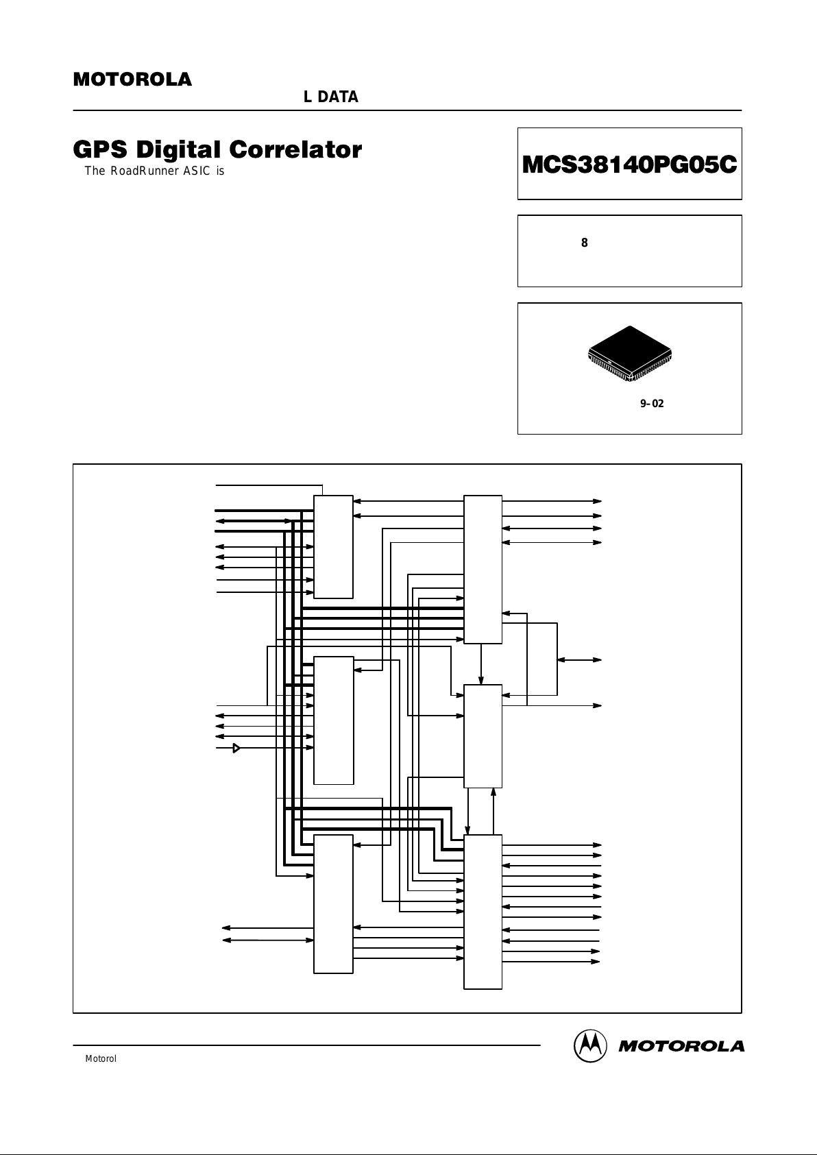
Top Level Block Diagram
ADDRESS
DATA
MPU CONTROL
C32KI
C32KO
RESET_L
GPIO
ALARM
RAM_CS_L
FS
DCD_IRQ_L
ONE_PPS
ST
UART_IRQ_L
FifL1
A/D
RTC_VDD
SCK_GPIO
MO_GPIO
MI_GPIO
SPI_IRQ_L
PWM1_GPIO
PWM2_GPIO
GPIO
GPIO
RXD_GPIO
CTS_GPIO
TXD_GPIO
RTS_GPIO
FS2_DTACKL
MPU_CLK
CS_L
OE_L
RAM_ROMCSL
CSL_VPAL
UART
RXD
CTS
TXD
RTS
WS(5:0)
MPU_SEL
DTACK_L
FS/2
RAM_CSL
C1KHZ
RTC_CSL
DCD_CSL
UART_CSL
GPIO_CSL
DIV3OR4
UART_CLK
FS/2 UC_EN
REAL
TIME CLOCK
8 CHANNEL
CORRELAT OR
GENERAL
PURPOSE I/O
CLOCK
GENERAT OR
MPU
INTERFACE
Order this document
by MCS38140PG05C/D
SEMICONDUCTOR TECHNICAL DATA
8 CHANNEL GPS
CORRELATOR
CASE 779–02
Motorola, Inc. 1997

MCS38140PG05C
2
MOTOROLA
1.0 Summary
The RoadRunner Application Specific Integrated Circuit
(ASIC) represents the 5th generation of Global Positioning
System (GPS) digital signal processing integrated circuits
used in Motorola commercial GPS products. When combined with an RF down converter, microprocessor, and
application software, it can become the heart of a broad line
of high performance and low cost GPS sensors. The
RoadRunner ASIC provides additional features and
achieves higher levels of performance at the same time
being a driver for the design of low cost GPS applications.
The RoadRunner ASIC contains circuitry to simultaneously track up to eight satellites. Each independent receiver
channel within the ASIC can be commanded to acquire and
continuously track a single spread spectrum signal using any
of the GPS gold codes or the FAA WAASS PN codes. The
ASIC performs the following major functions of a GPS
receiver:
• Samples the down converted IF signal with a 1 bit A/D
converter
• Down converts the signal to baseband by removal of the IF
the carrier frequency
• Signal de–spread with a replica PN code
• Doppler wipe off
• Provides digital in–phase and quadrature PROMPT and
EARLY–minus–LATE outputs
The microprocessor and software control each receiver
channel independently, and step the channel through the
satellite acquisition process until continuous track is
achieved. The acquisition and tracking functions are completely controlled by software, allowing for maximum flexibility for system enhancement and integration while
maintaining a cost effective implementation.
Digital signal processing software running in the microprocessor controls the satellite tracking function by closing both
code and phase/frequency tracking loops and converting the
ASIC outputs into pseudorange and pseudorange–rate
measurements, and decodes and stores the satellite broadcast ephemeris and clock correction data for use in down
stream data processing software. These measurements and
data are subsequently used in the receiver’s PVT software
(position, velocity, and time) in order to translate the range
measurements and ephemeris data into user position
coordinates.
The RoadRunner’s extended features include:
• Multiple microprocessor interface support (68330, 331,
332, 68HC000, 68EC000)
• Full in–phase and quadrature outputs on PROMPT and
EARLY minus LATE correlators
• Supports FAA WAASS PN codes
• Runs from 5.0 or 3.3 Volt power supply
• On–chip Real Time Clock
• On–chip UART
• Inexpensive 68 pin package
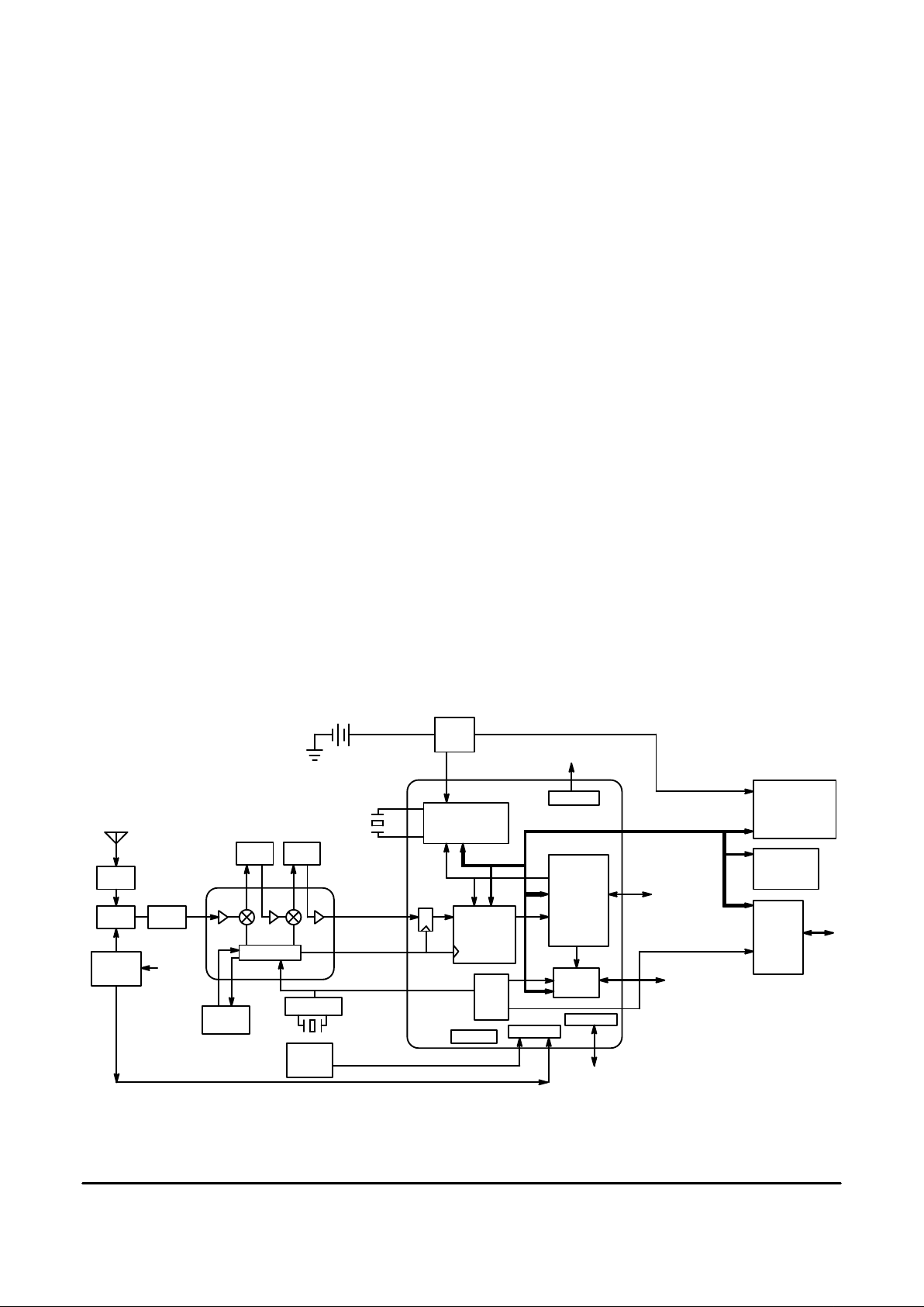
A top level block diagram of a typical GPS receiver using
the RoadRunner ASIC is detailed in Figure 1.1. Five major
subsystems are required to complete the design of a GPS
receiver. These subsystems include an antenna/LNA, a RF
downconverter (such as the Motorola MRFIC1502), a
reference oscillator, the RoadRunner ASIC, and a microprocessor/memory system. When the RoadRunner ASIC is
combined with the GT Oncore system software, the GPS
receiver will receive, track, and decode data from up to 8
parallel satellites to provide high performance position,
velocity, and time data to a user application.
AND
Figure 1.1 A Typical GPS Reciever Block Diagram with a RoadRunner ASIC
PLL / VCO
A/D
8 CHANNEL
CORRELATOR
CARRIER
FLASH ROM
128K X 8
128kX16
NON–VOLA TILE
RAM
32K X 8
128K X 8
REAL TIME CLOCK
32 kHz OSCILLATOR
LPF BPF
VCO
TUNE
BPF
BPF
LNA
MRFIC1502
REF OSCL
F–IF
MPU
INTERFACE
UART
MODULE
I/O PORT
MPU
68330
68331
68332
68000
68EC000
VRAM
MPU_CLK
A(7:0), D(7:0)
PWR
CLK
GEN
TEMP
SENSOR
SPI
GPIO
GLUELESS
INTERFACE
R/W, CS, ...
1–PPS
CURRENT
SENSOR
PWM’S
V
CC
SW
WIPEOFF
SAMPLE CLK
I/O
PORT

3
MCS38140PG05CMOTOROLA
2.0 I/O Description and Top Level Block Diagram
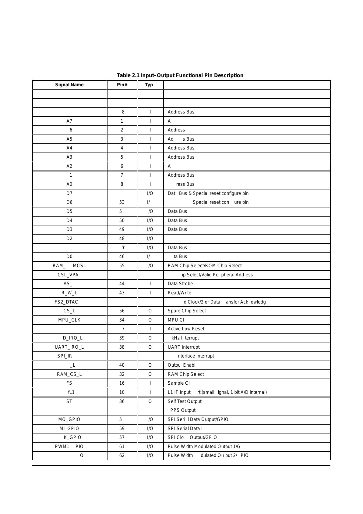
Table 2.1 provides a list of the functional pins of the ASIC
with the I/O type and a short description. Figure 2.1 shows
the top level block diagram of the ASIC showing the
connection of each pin to an internal functional block.
Table 2.1 Input–Output Functional Pin Description
Signal Name
Pin#
Type
Description
A23
66
I
Address Bus
A22
67
I
Address Bus
S21
68
I
Address Bus
A7
1
I
Address Bus
A6
2
I
Address Bus
A5
3
I
Address Bus
A4
4
I
Address Bus
A3
5
I
Address Bus
A2
6
I
Address Bus
A1
7
I
Address Bus
A0
8
I
Address Bus
D7
54
I/O
Data Bus & Special reset configure pin
D6
53
I/O
Data Bus & Special reset configure pin
D5
51
I/O
Data Bus
D4
50
I/O
Data Bus
D3
49
I/O
Data Bus
D2
48
I/O
Data Bus
D1
47
I/O
Data Bus
D0
46
I/O
Data Bus
RAM_ROMCSL
55
I/O
RAM Chip Select/ROM Chip Select
CSL_VPAL
42
I/O
RR Chip Select/Valid Peripheral Address
AS_L
44
I
Data Strobe
R_W_L
43
I
Read/Write
FS2_DTACKL
26
O
Sampled Clock/2 or Data Transfer Acknowledge
CS_L
56
O
Spare Chip Select
MPU_CLK
34
O
MPU Clock
RESET_L
27
I
Active Low Reset
DCD_IRQ_L
39
O
1 kHz Interrupt
UART_IRQ_L
38
O
UART Interrupt
SPI_IRQ_L
37
O
SPI Interface Interrupt
OE_L
40
O
Output Enable
RAM_CS_L
32
O
RAM Chip Select
FS
16
I
Sample Clock Input
FifL1
10
I
L1 IF Input Port (small signal, 1 bit A/D internal)
ST
36
O
Self Test Output
ONE_PPS
35
O
1PPS Output
MO_GPIO
58
I/O
SPI Serial Data Output/GPIO
MI_GPIO
59
I/O
SPI Serial Data Input/GPIO
SCK_GPIO
57
I/O
SPI Clock Output/GPIO
PWM1_GPIO
61
I/O
Pulse Width Modulated Output 1/GPIO
PWM2_GPIO
62
I/O
Pulse Width Modulated Output 2/GPIO
 Loading...