

Page 1

MCPN750A CompactPCI
Single Board Computer
Installation and Use
MCPN750A/IH5
September 2001 Edition
Page 2

© Copyright 2001 Motorola, Inc.
All Rights Reserved.
Printed in the United States of America.
Motorola and the stylized M logo are registered trade marks of Motoro la, Inc.
PowerPC is a registered trademark of International Business Machines and is used by
Motorola Inc. under license from IBM Corporation.
CompactPCI is a registered trademark of PCI Industrial Computer Manufacturers Group.
All other product or se rvice names mentioned i n this document are trademarks or registered
trademarks of their respective holders.
Page 3

Safety Summary
The following general safety precautions must be observed during all phases of operation, service, and repair of this
equipment. Failure to comply with these precautions or with specific warnings elsewhere in this manual could result
in personal injury or damage to the equipment.
The safety precaut ions listed be low represent warnings of ce rtain danger s of which Mot orola is awar e. You, as the
user of the product, should follow these warnings and all other safety precautions necessary for the safe operation of
the equipment in your operating environment.
Ground the Instrument.
To minimize shock hazard, the equipment chassis and enclosure must be connected to an electrical ground. If the
equipment is su pplied wi th a three-c onductor A C power ca ble, the po wer cable m ust be plug ged into an a pproved
three-contact electrical outlet, with the grounding wire (green/yellow) reliably connected to an electrical ground
(safety ground) at the power outlet. The power jack and mating plug of the power cable meet International
Electrotechnical Commission (IEC) safety standards and local electrical regulatory codes.
Do Not Operate in an Explosive Atmosphere.
Do not operate the equipment in any explosive atmosphere such as in the presence of flammable gases or fumes.
Operation of any electrical equipment in such an environment could result in an explosion and cause injury or damage.
Keep Away From Live Circuits Inside the Equipment.
Operating personnel must not remove equipment covers. Only Factory Authorized Service Personnel or other
qualified service personnel may remove equipment covers for internal subassembly or component replacement or any
internal adjust ment. Service pe rsonnel should n ot replace compon ents with power c able connected. Under certain
conditions, dangerous voltages may exist even with the power cable removed. To avoid injuries, such personnel
should always disconnect power a nd discharge circuits bef ore touching components.
Use Caution When Exposing or Handling a CRT.
Breakage of a Cathode-Ray Tube (CRT) causes a high-velocity scattering of glass fragments (implosion). To prevent
CRT implosion, do not handl e the CRT and avoid rough handling o r jarring of t he equipment . Handling o f a CRT
should be done only by qualified service personnel using approved safety mask and gloves.
Do Not Substitute Parts or Modify Equipment.
Do not install substitute parts or perform any unauthorized modification of the equipment. Contact your local
Motorola representative for service and repair to ensure that all safety features are maintained.
Observe Warnings in Manual.
W arn ings , such as th e exa mple be low, preced e pote ntia lly da nger ous pro cedure s thro ugh out th is manual . In struc tion s
contained in the warnings m ust be follow ed. You should also employ all ot her safety precautions w hich you dee m
necessary for the operation of the equ ipment in your oper at ing environment.
To prevent serious injury or death from dangerous voltages, use extreme
caution when handling, testing, and adjusting this equipment and its
Warning
components.
Page 4

Flammability
All Motorola PWBs (printed wiring boards) are manufactured with a flammability rating
of 94V-0 by UL-recognized manufacturers.
EMI Caution
This equipment ge ner ates, uses a nd can radi ate el ectro magne tic energy . It
!
Caution
This product contains a lithium battery to power the clock and calendar circuitry.
!
Caution
may cause or be susceptible to electromagnetic interference (EMI) if not
installed and used with adequate EMI protection.
Lithium Battery Caution
Danger of explosion if battery is re placed incorrect ly. Replace battery only
with the same or equivalent type recommended by the equipment
manufacturer. Dispose of used batteries according to the manufacturer’s
instructions.
!
Attention
!
Vorsicht
Il y a danger d’explosion s’il y a remplacement incorrect de la batterie.
Remplacer uniquement avec une batterie du même type ou d’un type
équivalent recommandé par le constructeur. Mettre au rebut les batteries
usagées conformément aux instructions du fabricant.
Explosionsgefahr bei unsachgemäßem Austausch der Ba tt erie. Ersatz nur
durch denselben ode r einen vom Herstel ler empfohle nen Typ. Entsorgu ng
gebrauchter Batterien nach Angaben des Herstellers.
Page 5

CE Notice (European Community)
This is a Class A product. In a domestic environment, this product may
!
Warning
Motorola Compute r Group pro ducts wi th the CE mar king co mply with the EMC Dir ective
(89/336/EEC). Compliance with this directive implies conformity to the following
European Norms:
EN55022 “Limits and Methods of Meas urement of Radio Int erferen ce Chara cteri stic s
of Information Technology Equipment”; this product tested to Equipment Class A
EN55024 “Information Technology Equipment-Immunity characteristics-Limits and
methods of measurement”
Board products are tested in a representative system to show compliance with the above
mentioned requirements. A proper installation in a CE-marked system will maintain the
required EMC /safety performance.
In accordance with European Community directives, a “Declaration of Conformity” has
been made and is available on request. Please contact your sales representative.
cause radio interference, in which case the user may be required to take
adequate measures.
Notice
While reasonable efforts have been made to assure the accuracy of this document,
Motorola, Inc. a ssumes n o lia bility r esulti ng from any omissio ns in this docu ment, or from
the use of the information obtained therein. Motoro la reserves th e right to revise this
document and to ma ke c hanges from time to ti me in t h e cont ent hereof without obligation
of Motorola to notify any person of such revision or changes.
Electronic versions of this material may be read online, downloaded for personal use, or
referenced in another document as a URL to the Motorola Computer Group website. The
text itself may not b e published commerci ally in print o r electronic for m, edited, transla ted,
or otherwise altered without the permiss ion of Motorola, Inc.
It is possible th at t hi s publication may contain r ef erence to or information about Motorola
products (machines and pr ograms), progra mming, or services that are not av ailable in your
country. Such references or information must not be construed to mean that Motorola
intends to announce such Motorola products, programming, or services in your country.
Page 6

Limited and Restricted Rights Legend
If the documentation contained herein is supplied, directly or indirectly, to the U.S.
Government, the following notice shall apply unless otherwise agreed to in writing by
Motorola, Inc.
Use, duplication, or disclosure by the Government is subject to restrictions as set forth in
subparagraph (b)(3) of t he Rig hts i n Tech nical Data clause at DFARS 252.227-7013 (Nov.
1995) and of the Rights in Noncommerc ial Computer Software and Docume ntation clause
at DFARS 252.227-7014 (Jun. 1995).
Motorola, Inc.
Computer Group
2900 South Diablo Way
Tempe, Arizona 85282
Page 7

Contents
About This Manual
Summary of Changes...............................................................................................xviii
Overview of Contents..............................................................................................xviii
Comments and Suggestions.....................................................................................xviii
Conventions Used in This Manual.............................................................................xix
CHAPTER 1 Hardware Preparation and Installation
Introduction ................................................................................................................1-1
Product Description............................................................................................1-1
Block Diagram....................................................................................................1-1
Getting Started ..................................................................................... ......................1-3
Overview of Start-up Procedure.........................................................................1-3
Equipment Required...........................................................................................1-4
Unpacking Instructions.......................................................................................1-5
ESD Precautions.................................................................................................1-5
Preparation.................................................................................................................1-6
Hardware Configuration.....................................................................................1-6
MCPN750A Base Board Preparation.................................................................1-6
Flash Bank Selection (J7)............................................................................1-7
Stand-Alone Operating Mode (J8) ..............................................................1-8
System Considerations......................................................................................1-10
TMCPN710 Transition Module Preparation ....................................................1-11
Serial Ports 1 and 2 ....................................................................................1-13
COM3 and COM4 Asynchronous Serial Ports..........................................1-15
TM-PIMC-0001 Transition Module Preparation..............................................1-16
COM 1 and COM 2 Asynchronous Serial Ports........................................1-18
COM3 and COM4 Asynchronous Serial Ports..........................................1-20
Hardware Installation...............................................................................................1-21
Installing PMC Modules on the MCPN750A SBC..........................................1-21
Installing the MCPN750A Baseboard..............................................................1-24
Installing a TMCPN710 or TM-PIMC-0001 Transition Module.....................1-26
Installing PIMs on the TM-PIMC-0001 Transition Module .....................1-26
Installing the Transition Module in the Chassis........................................1-28
MCPN750A Module Power Requirements .............................................................1-31
vii
Page 8

CHAPTER 2 Startup and Operation
Introduction ...............................................................................................................2-1
Applying Power.........................................................................................................2-1
Memory Maps......................................................................... ...................................2-3
Processor Memory Map ....................................................... ...... ........................2-3
Default Processor Memory Map.................................................................2 -3
PCI Local Bus Memory Map.............................................................................2-4
CompactPCI Memory Map................................................................................2-5
Address Decoding with the 21554..............................................................2-5
L2 Cache.............................................................................................................2-6
System Clock Generator.....................................................................................2-6
PPC Bus Arbitration...........................................................................................2-6
PCI Host Bridge .................................................................................................2-6
PCI Arbitration...................................................................................................2-8
Interrupt Handling..............................................................................................2-8
ISA DMA Channels ...........................................................................................2 -9
Sources of Reset.................................................................................................2-9
Power-On Reset ........................................................................................2-11
Undervoltage Reset...................................................................................2-11
Front Panel Push Button Reset..................................................................2-11
CompactPCI Reset (RST#).......................................................................2-11
Watchdog Timer Reset..............................................................................2-11
Software Resets.........................................................................................2-12
Reset Source Identification.......................................................................2-12
Endian Issues....................................................................................................2-12
Processor/Memory Domain ......................................................................2-12
PCI Domain...............................................................................................2-13
CHAPTER 3 PPCBug
PPCBug Overview.....................................................................................................3-1
PPCBug Basics..........................................................................................................3-1
Memory Requirements.............................................. ...... ...................................3-3
PPCBug Implementation....................................................................................3-3
MPU, Hardware, and Firmware Initialization...........................................................3-3
Using PPCBug...........................................................................................................3-5
Debugger Commands.........................................................................................3-6
Diagnostic Tests................................................................................................3-10
viii
Page 9

CHAPTER 4 CNFG and ENV Commands
Overview....................................................................................................................4-1
CNFG - Configure Board Information Block............................................................4-2
ENV - Set Environment.............................................................................................4-3
Configuring the PPCBug Parameters.................................................................4-3
CHAPTER 5 Remote Start Via the PCI Bus
Introduction................................................................................................................5-1
Overview.............................................................................................................5-1
Command/response Register Description...........................................................5-3
Opcode 0x01: Write/Read Virtual Register........................................................5-5
Opcode 0x02: Initialize Memory........................................................................5-5
Opcode 0x03: Write/Read Memory....................................................................5-6
Opcode 0x04: Checksum Memory.....................................................................5-6
Opcode 0x05: Memory Size Query....................................................................5-7
Opcode 0x06: Debugger Query..........................................................................5-7
Opcode 0x07: Execute Code...............................................................................5-7
Command/Response Channel Error Codes.........................................................5-8
Demonstration of the Host Interface...................................................................5-9
Reference Function: srom_crc.c.......................................................................5-12
CHAPTER 6 Functional Description
Introduction................................................................................................................6-1
Features......................................................................................................................6-1
General Description ...................................................................................................6-2
Block Diagram...........................................................................................................6-3
CompactPCI Bus Interface.................................................................................6-5
Ethernet Interface................................................................................................6-6
PCI Mezzanine Interface ....................................................................................6-7
ISA Bus Devices.................................................................................................6-8
Asynchronous Serial Ports...........................................................................6-8
Configuration and Status Registers.............................................................6-8
Serial EEPROM..................................................................................................6-8
PCI Peripheral Bus Controller (PBC).................................................................6-9
ISA Interface................................................................................................6-9
EIDE Interface...........................................................................................6-10
USB Interface............................................................................................6-10
ISA Interrupt Controller............................................................................6-10
ix
Page 10

ISA DMA Channels..................................................................................6-10
Interval Timers..........................................................................................6-11
Real-Time Clock/NVRAM/Watchdog Timer Function...................................6-11
Replacing Lithium Batteries .....................................................................6-12
Hot Swap Control Circuitry .............................................................................6-14
Programmable Timers......................................................................................6-14
Raven General Purpose Timers.................................................................6-14
Raven Watchdog Timers........................................................... ................6-15
M48T559 Watchdog Timer.......................................................................6-15
Interval Timers..........................................................................................6-16
Serial Port Signal Multiplexing........................................................................6-16
I/O Signal Multiplexing (IOMX)..............................................................6-17
Signal Descriptions ...................................................................................6-19
ABORT(ABT)/RESET (RST) Switch (S1)......................................................6-19
Front Panel Indicators (DS1 - DS3)................................................................. 6-20
MPC750 Processor...................................................................................... .....6-20
Raven PCI-Host Bridge...................................... ...... ..... ............................6-20
Flash Memory ...........................................................................................6-20
JTAG/COP................................................................................................6-21
Bank A Flash Programming Enable..........................................................6-21
ECC Memory Controller.................................................................................. 6-22
DRAM Memory ............................................. ..... ........................................ .....6-22
Compact FLASH Memory Card ......................................................................6-22
TMCPN710 Transition Module .......................................................................6-23
TM-PIMC-0001............................................................... .................................6-23
CHAPTER 7 Connector Pin Assignments
MCPN750A and Transition Module Connectors ......................................................7-1
MCPN750A Connector Pin Assignments.................................................................7-2
MCPN750A CompactPCI Bus Connectors (J1/J2)............................................7-2
MCPN750A CompactPCI User I/O Connector J3.............................................7-4
MCPN750A Connector J4..................................................................................7-6
MCPN750A CompactPCI User I/O Connector (J5)..........................................7-7
MCPN750A PCI Mezzanine Card Connectors
(J11/21, J12/22, J13/23, J14/24..........................................................................7-9
MCPN750A 10BaseT/100BaseTx Connector (J18) ........................................7-12
MCPN750A Debug Connector (J19)...............................................................7-12
MCPN750A Processor RISCWatch Debug Connector (J6).............................7-17
TMCPN710 Transition Module....................... ...... ..... ........................................ .....7-18
TMCPN710 Transition Module CompactPCI Connectors (J3/J4/J5)..............7-18
x
Page 11

TMCPN710 Transition Module COM1 Connector (J6)...................................7-19
TMCPN710 Transition Module COM2 Connector (J8)...................................7-20
TMCPN710 Transition Module COM3 Header (J11)......................................7-20
TMCPN710 Transition Module COM4 Header (J14)......................................7-21
TMCPN710 Transition Module 10BaseT/100BaseTx Connector (J13) ..........7-22
TMCPN710 Transition Module USB Connectors (J10, J12)...........................7-23
TMCPN710 Transition Module IDE Compact FLASH Connectors
(J15, J16)...........................................................................................................7-23
TMCPN710 Transition Module PMC I/O Connectors (J1/J2).........................7-25
TM-PIMC-0001 Transition Module ........................................................................7-27
TM-PIMC-0001 CompactPCI User I/O Connector (J3, J4, & J5)...................7-27
TM-PIMC-0001 Transition Module COM1 Connector (J9)............................7-28
TM-PIMC-0001 Transition Module COM2 Connector (J8)............................7-29
TM-PIMC-0001 Transition Module COM3 and COM4 Connectors
(J12 & J13)........................................................................................................7-30
TM-PIMC-0001 Transition Module 10BaseT/100BaseTx Connector (J7)......7-31
TM-PIMC-0001 Transition Module IDE Compact FLASH Connector (J1)....7-31
TM-PIMC-0001 Transition Module PMC I/O Connectors
(J10, J20, and J14/J24)......................................................................................7-33
APPENDIX A Specifications
Specifications............................................................................................................A-1
Cooling Requirements ..............................................................................................A-2
EMC Compliance......................................................................................................A-3
APPENDIX B Related Documentation
Motorola Computer Group Documents....................................................................B-1
Manufacturers’ Documents.......................................................................................B-2
Related Specifications...............................................................................................B-4
xi
Page 12

xii
Page 13

List of Figures
Figure 1-1. MCPN750A Base Board Block Diagram................................................1-2
Figure 1-2. MCPN750A Switches, Headers, Connectors, Fuses, LEDs ................... 1-9
Figure 1-3. TMCPN710 Connector and Header Locations .....................................1-12
Figure 1-4. MCPN750A/TMCPN710 Serial Ports 1 and 2 .....................................1-14
Figure 1-5. TMCPN710 Serial Ports 3 and 4 ...........................................................1-15
Figure 1-6. TM-PIMC-0001 Connector and Header Locations...............................1-17
Figure 1-7. MCPN750A/TM-PIMC-0001 Serial Ports 1 and 2...............................1-19
Figure 1-8. TM-PIMC-0001 Serial Ports 3 and 4....................................................1-20
Figure 1-9. PMC Module Placement on MCPN750A.............................................1-22
Figure 1-10. TMCPN710 or TM-PIMC-0001/MCPN750A Mating Configuration1-30
Figure 2-1. PPCBug System Startup..........................................................................2-2
Figure 6-1. MCPN750A Block Diagram...................................................................6-4
Figure 6-2. Serial Port Signal Multiplexing.............................................................6-17
Figure 6-3. MX Signal Timings...............................................................................6-19
xiii
Page 14

xiv
Page 15

List of T ables
T ab le 1-1. Startup Overview................................................................................. .....1-3
T ab le 1-2. Installing a PIM on the TM-PIMC-0001 T ransi tion Module.................1-27
Table 2-1. Processor Default View of the Memory Map ...........................................2-3
Table 2-2. Classes of Reset and Effectiveness.........................................................2-10
T ab le 3-1. Debugger Command s........................................ .......................................3-7
Table 3-2. Diagnostic Test Groups...........................................................................3-11
Table 5-1. Command/Respond Error Codes..............................................................5-8
T ab le 6-1. MCPN750A Features........................ ..... ...... ........................................ .....6-1
Table 6-2. Multiplexing Sequence of the MX Function..........................................6-18
Table 7-1. MCPN750A J1 CompactPCI Connector..................................................7-2
Table 7-2. MCPN750A J2 CompactPCI Connector..................................................7-3
Table 7-3. MCPN750A J3 User I/O Connector.........................................................7-5
Table 7-4. MCPN750A J5 User I/O Connector.........................................................7-7
T ab le 7-5. MCPN750A PCI Mezzanine Card Connector..........................................7-9
T ab le 7-6. MCPN750A PCI Mezzanine Card Connector........................................7-10
Table 7-7. MCPN750A 10BaseT/100BaseTx Connector J18 .................................7-12
Table 7-8. MCPN750A Debug Connector (J19)......................................................7-13
Table 7-9. MCPN750A RISCWatch Debug Connector (J6)....................................7-17
T ab le 7-10. TMCPN710 COM1 Connector (J6)............................ ...... ....................7-19
T ab le 7-11. TMCPN710 COM2 Connector (J8)...................... ................................7-20
T ab le 7-12. TMCPN710 COM3/COM4 Headers....................................................7-20
Table 7-13. TMCPN710 10BaseT/100BaseTx Connector (J13).............................7-22
Table 7-14. TMCPN710 USB 0 Connector (J10)....................................................7-23
Table 7-15. TMCPN710 USB 1 Connector (J12)....................................................7-23
Table 7-16. TMCPN710 Compact FLASH IDE Connectors...................................7-24
Table 7-17. TMCPN710 PMC 1 and 2 I/O Connector ............................................7-25
Table 7-18. TM-PIMC-0001 COM1 Connector (J9)...............................................7-28
Table 7-19. TM-PIMC-0001 COM2 Connector (J8)...............................................7-29
Table 7-20. TM-PIMC-0001 COM3 and COM4 Headers.......................................7-30
Table 7-21. TM-PIMC-0001 10BaseT/100BaseTx Connector (J7).........................7-31
Table 7-22. TM-PIMC-0001 CompactFLASH IDE Connector (J1) .......................7-32
Table 7-23. TM-PIMC-0001 PMC I/O Module 1 (PIM1) - Host I/O
Connector Pin Assignments.....................................................................................7-33
Table 7-24. TM-PIMC-0001 PMC I/O Module 2 (PIM2) - Host I/O
Connector Pin Assignments.....................................................................................7-34
xv
Page 16

Table 7-25. PMC I/O Modules 1 and 2 (PIM1 a nd PIM2) -
PMC I/O Connector Pin Assignments.....................................................................7-36
Table A-1. MCPN750 Specifications ......................................................................A-1
Table B-1. Motorola Computer Group Documents ................................................. B-1
Table B-2. Manufacturers’ Documents ................................................................... B-2
Table B-3. Related Specifications ........................................................................... B-4
xvi
Page 17

About This Manual
This manual, MCPN750A CompactPCI Single Board Computer
Installation and Use (MCPN750A/IH5) provides general information,
hardware preparati on and installation instr uct i ons, operating instructi ons,
firmware informatio n, functional descriptions, and pin assig nments for the
MCPN750A family of Single Board Computers. In addition, sufficient
information is a lso provided for the two t ransition modules manufactured
by Motorola for use with the MCPN750A (TMCPN710 and TM-PIMC-
0001). The document should be used by anyone who wants general , as well
as technical information about the MCPN750A products.
Note: This revision of the MCPN750A Installation and Use manual
supersedes all previous versions of this document.
Currently, the boards are provided in the following configurations:
Part Number Description
MCPN750-1222 A MPC750, 266MHz, 16MB ECC DRAM, 5MB FLASH, 1MB L2 Cache
MCPN750-1232 A MPC750, 266MHz, 32MB ECC DRAM, 5MB FLASH, 1MB L2 Cache
MCPN750-1332 A MPC750, 366MHz, 32MB ECC DRAM, 5MB FLASH, 1MB L2 Cache
MCPN750-1342 A/B MPC750, 366MHz, 64MB ECC DRAM, 5MB FLASH, 1MB L2 Cache
MCPN750-1352 A/B MPC750, 366MHz, 128MB ECC DRAM, 5MB FLASH, 1MB L2 Cache
MCPN750-1362 A MPC750, 366MHz, 256MB ECC DRAM, 5MB FLASH, 1MB L2 Cache
MCPN750-1442 A MCP750, 466MHz, 64MB ECC DRAM, 5MB FLASH, 1M B L2 Cache
MCPN750-2342 A/B MPC750, 366MHz, 64MB ECC DRAM, 5MB FLASH, 1MB L2 Cache,
Transition Module, Ethernet Rear I/O
MCPN750-2352 A/B MPC750, 366MHz, 128MB ECC DRAM, 5MB FLASH, 1MB L2 Cache,
Transition Module, Ethernet Rear I/O
MCPN750-2352 A-F MPC750, 366MHz, 128MB EC C DRAM, 5MB FLASH, 1MB L2 Cache,
Transition Module, Ethernet Rear I/O
MCPN750-2362 A/B MPC750, 366MHz, 256MB ECC DRAM, 5MB FLASH, 1MB L2 Cache,
Transition Module, Ethernet Rear I/O
xvii
Page 18

Summary of Changes
The followi ng is a list of cha nges made since the last release of this
manual.
Date Changes Replaces
09/01 Updated table of model numbers
preceeding this section.
Reinserted information left out of IH4
version of manual, which included
information on MCPN750A, the
TMCPN710 and the TM-PIMC-0001,
instead of the earlier MCPN750. Also,
included J8 jumper settings for StandAlone operation.
07/00 68-pin .08 Series Submi nature D PMC I/O
Connector.
Previously listed model numbers.
68-pin .050 Series Subminature
D PMC I/O Connector.
Overview of Contents
This section provides a brief overview of each chapte r and appendix within
this document.
xviii
Chapter 1, Hardware Preparation and Installation, provides a brief
product description and a block diagram. The remainder of the chapter
provides information on hardware preparation and installation
instructions, including peripheral boards such as the TMCPN710 or TMPIMC-0001 Transition Module.
Chapter 2, Startup and Ope ration, provides an o verview of basic oper ating
and configuring issues such as the PPCBug firmware, the memory maps,
interrupts, arbitration, sources of reset and endian issues.
Chapter 3, PPCBug, provides an overview and description of basic
PPCBug use including implement ation issues, a list of the initialization
sequence, a description of basic debugger commands, as well as a list of
diagnostic tests typically run.
Page 19

Chapter 4, CNFG and ENV Commands, provides an ex planation of two of
the more important PPCBug configuration commands: CNFG and ENV.
Includes information on how to configure the VMEbus and PCI bus
environments using the ENV command.
Chapter 5, Remote Start Via the PCI Bus, provides a description of the
remote start capability th at is availabl e via the PCI bu s using PPCBug
commands.
Chapter 6, Functional Description, provides a description of the major
components and functionality of the MCPN750A.
Chapter 7, Connector Pin Assignments, provides a listing of all major
connector pinout information for the MCPN750A, the TMCPN710, and
TM-PIMC-0001.
Appendix A, Specifications, provides basic board specification
information including recommendations on cooli ng and EMC compliance.
Appendix B, Related Documentation, provides a listing of related
motorola and vendor documentation, as well as a list of related industry
standard specifications.
Comments and Suggestions
Motorola welcomes and appreciates your comments on its doc umentation.
We want to know what y ou think about our manuals and how we can make
them better. Mail comments to:
Motorola Computer Group
Reader Comments DW164
2900 S. Diablo Way
Tempe, Arizona 85282
You can also submit comments to the following e-mail address:
reader-comments@mcg.mot.com
xix
Page 20

In all your corres pondence , plea se li st your name, po si tion, a nd compan y.
Be sure to include the title and par t number of the manual and tell how you
used it. Then tell us your feelings about its strengths and weaknesses and
any recommendations for improvements.
Conventions Used in This Manual
The following typographical conventions are used in this document:
bold
is used for user inpu t that you t ype just as i t appears ; it is al so used for
commands, options and arguments to commands, and names of
programs, directories and files.
italic
is used for names of variables to which you assign values. Italic is also
used for comments in screen dis plays and examples, and to intr odu ce
new terms.
courier
is used for system output (for example, screen displays, reports),
examples, and system prompts.
xx
<Enter>, <Return> or <CR>
<CR> represents the carriage return or Enter key.
CTRL
represents the Control key. Execute control characters by pr essing the
Ctrl key and the letter simultaneously, for example, Ctrl-d.
Page 21

1Hardware Preparation and
Introduction
This chapter provides startup and safety instructions related to this
product, hardware preparation instructions - including default jumper
settings, system considerations, and installation instructions for the
baseboard, as well as the PMCs and t ransition modules associate d with this
board.
A fully implemented MCPN750A consists of the baseboard plus:
❏ One or two optional PCI mezzanine cards (PMC) for additional
versatility
❏ One of two different types of optional transition modules: the
TMCPN710 or the TM-PIMC-0001 for added I/O flexibility
Product Description
The MCPN750A is a hot swappa ble CompactP CI, non-sys tem slot, single
board computer based on the PowerPlus architecture. It consists of the
MPC750 processor with L2 cache, the Raven PCI Bridge and Interrupt
Controller, the ECC Memory Controller Falcon chipset , 5MB of linea r
Flash memory, 16MB to 256MB of ECC protecte d DRAM, i nterf ac e t o a
CompactPCI bus, and several I/O peripherals.
Installation
1
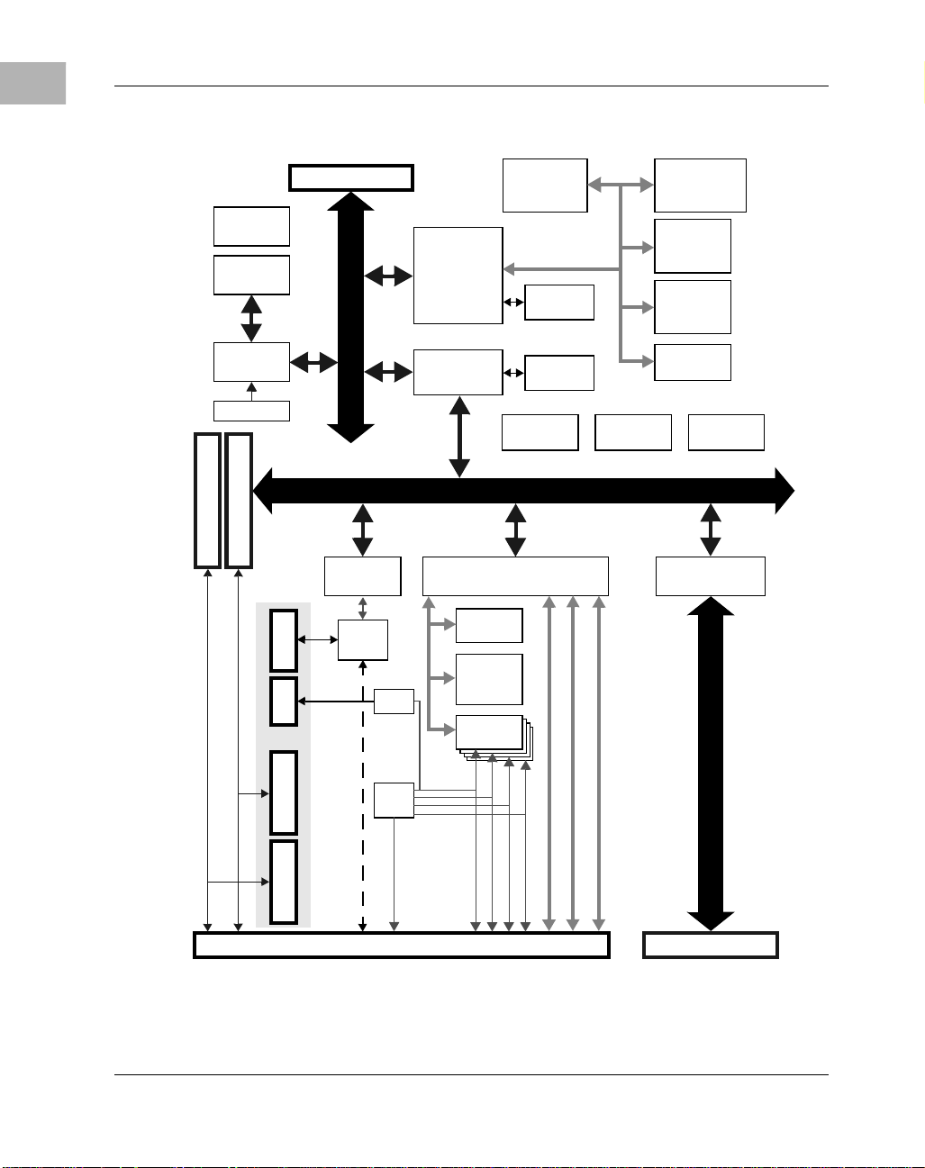
Block Diagram
The block diagram in Figure 1-1 illustrates the architecture of the
MCPN750A baseboard.
1-1
Page 22
1
Hardware Preparation and Installation
Arbitration
Control
L2 Cache
1M
Processor
MPC750
Core Power
32/64-bit PMC Slot 2
32/64-bit PMC Slot 1
Debug Connector
Ethernet
Intel 21143
EthernetSerialPMC Slot 2PMC Slot 1
100BTx
Bus
66MHz PPC603 Processor
10BT/
RS232
16M/64M/128M
Memory
Controller
Falcon 3
Chipset
PCI Bridge
& MPIC
Raven 5 ASIC
33MHz 32/64-bit PCI
PBC
VT82C586B
ISA
Registers
ISA
NVRAM/
WD/RTC
MK48T559
UARTs
16C550C
DRAM
(Bank 1)
SROM
AT24C04
Interrupt
Serializer
Clock
Generator
USB0
Local Bus
USB1
EIDE
Reset
Control
DRAM
(Bank 2)
16M/64M/128M
Flash
(soldered)
4M
Flash
(socketed)
1M
System
Registers
Hot Swap
Control
PCI-PCI BRIDGE
Intel 21554
Bus
IOMX
33MHz 32/64-bit CompactPCI
SERIAL 2
SERIAL 3
SERIAL 4
(OPTIONAL ROUTING TO TM)
SERIAL 1
CompactPCI J1/J2User I/O J3 & J5
Figure 1-1. MCPN750A Baseboard Block Diagram
1-2 Computer Group Literature Center Web Site
Page 23

Getting Started
Getting Started
This section provides an overview of the steps necessary to install and
power up the MCPN750A, any additional equipment requirements, and a
brief section on unpacki ng and ESD precautio ns. As identified in the table
below, several steps can be omitted if your board, for example, has been
shipped with PMCs and Flash already installed
Overview of Start-up Procedure
The following table li sts the th ings you will need to do bef ore you can use
this board and t ells where to find the infor mation you n eed to perform e ach
step. Be sure to rea d this entire c hapter, incl uding all Caution and Warning
notes, before you begin.
Table 1-1. Startup Overview
Task Section or Manual Reference Page
Unpack the hardware. Unpacking Instructions 1-5
Configure the hardware by
setting jumpers on the baseboard
and transition module.
Ensure CompactFlash card is
installed (if required)
Install the PMC Module (if
required)
Install the MCPN750A in the
chassis.
Install the transition module in
the chassis.
Connect any other equipment
you will be using .
Power up the system. Applying Power 2-1
MCPN750A Baseboard Preparation and
TMCPN710 or TM-PIMC-0001 Transition Module
Preparation
Compact Flash Memory Card Installation 1-6
PMC Module Installation 1-21
MCPN750A CompactPCI SBC Installation 1-24
TMCPN710 or TM-PIMC-0001 Transition Module
Installation
Connector Pin Assignments 7-1
For more information on optional devices and
equipment, refer to the d ocumentation provided with
the equipme nt .
1
1-6, 1-11,
and 1-16
1-26
http://www.motorola.com/computer/literature 1-3
Page 24

1
Hardware Preparation and Installation
Table 1-1. Startup Overview (Continued)
Task Section or Manual Reference Page
Note that the debugger in itializes
the MCPN750A
Initialize the system clock. Using the Debugger, Debugger Commands, the
Examine and/or change
environmental parameters.
Program the bo a r d as ne e de d for
your applications.
Using PPCBug 3-5
You may also wish to obtain the PPCBug Firmware
Package User’s Manual, listed in Appendix B,
Related Documentation.
SET command
CNFG and ENV Commands 4-2
MCPN750A CompactPCI Single Board Computer
Programmer’s Reference Guide, listed in Appendix
B, Related Documentation.
B-1
3-6
and 4-3
B-1
Equipment Required
The following equipment is required to complete an MCPN750A system:
❏ CompactPCI system enclosure
❏ System console terminal
❏ Operating system (and/or application software)
❏ Disk drives (and/or other I/O) and controllers
❏ Transition module (TMCPN710 or TM-PIMC-0001) and
connecting cables
MCPN750A baseboards are factory-configured for I/O handling via a
TMCPN710 or TM-PIMC-0001 transition module. There are currently
eight MCPN750A models corresponding to the five separate memory
configurations, t wo p rocessor spee ds and fron t or rea r et hernet I/O. Eith er
one of the aforementioned transition modules support all models of the
baseboard. Refer to the subsections on the MCPN750A and transition
module installation for more information.
1-4 Computer Group Literature Center Web Site
Page 25

Unpacking Instructions
Note If the shipping carton is damaged upon receipt, request that
the carrier’s agent be present during the unpacking and
inspection of the equipment.
Unpack the equipment from the shipping carton. Refer to the packing list
and verify that al l items are present . Sa ve t he packing material for storing
and reshipping of equipment.
Getting Started
1
!
Caution
Avoid touching areas of integrated circuitry; static discharge can damage
circuits.
ESD Precautions
Motorola strongly recommends that you use an antistatic wrist strap and a
conductive foam pad when installing or upgrading a system. Electronic
components, such as di sk driv es, comput er boar ds, and memory mod ules, c an
be extremely sensitive to ESD. After removing the component from the system
or its protective wrapper, place the component flat on a grounded, static-free
surface (and in the case of a board, component side up). Do not slide the
component over any surface.
If an ESD station is not available, you can avoid damage resulting from ESD
by wearing an antistatic wrist strap (available at electronics stores) that is
attached to an unpainted metal part of the system chassis.
Inserting or removing modules with power applied may result in damage
!
Caution
to module components.
Dangerous voltages, capable of causing death, are present in
!
Warning
http://www.motorola.com/computer/literature 1-5
this equipment. Use extreme caution when handling, testing,
and adjusting.
Page 26

1
Hardware Preparation and Installation
Preparation
This section discusses certain hardware and software tasks that may need
to be performed prior to installing the board in a CompactPCI chassis.
Hardware Configuration
To produce the desired configuration and ensure proper operation of the
MCPN750A, you may need to carry out certain hardware modifications
before installing the module.
The MCPN750A provides software control over most options by setting
bits in control registers after installing the module in a system. You can
also modify the board’s configuration by modifying similar control
registers. The MCPN750A control registers are described in the
MCPN750A CompactPCI Single Board Computer Programmer’s
Reference Guide (MCPN750A/ PG), whi ch can be accessed on line i n pd f
or html format through the Moto rola Comput er Group Liter ature web site
(http://www.motorola.c om/comp uter/li tera ture).
Some options, however, are not software-programmable. These options
are controlled by installing or removing header jumpers or interface
modules on the baseboard or the associated transition module.
MCPN750A Baseboard Preparation
Figure 1-2 illustrates the placement of the switches, jumper headers,
connectors, and LED indicat ors on the MCPN750A. Manua lly configured
items on the baseboard include:
❏ Flash bank selection (J7)
❏ Stand-Alone Operating Mode (J8)
For a discussion of the configu red ite ms on th e trans itio n module , re fer in
this chapter to the sections titled TMCPN710 Transition Module
Preparation, or to the respec tive user’s manual s for the transit ion modules
(listed in the Related Documentation appendix) as necessary.
1-6 Computer Group Literature Center Web Site
Page 27
The MCPN750A is factory tested and shipped with the configurations
described in the following sections. The MCPN750A’s required and
factory-installed debug monitor, PPCBug, operates with those factory
settings.
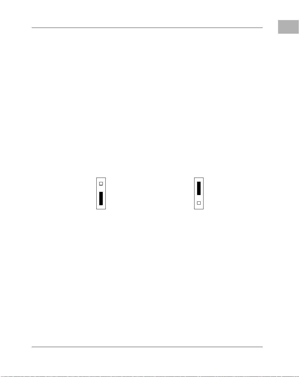
Flash Bank Selection (J7)
The MCPN750A baseboard has provision for 1MB of 16-bit Flash
memory and 4MB of linear Flash memory.
The Flash memory is organized in two banks, Bank A is 64 bits wide and
Bank B is 16 bits wide. Bank B contains the onboard debugger, PPCBug.
To enable Flash Bank A, place a j umper acr oss he ader J 7 pins 1 and 2. T o
enable Fla sh Bank B (1MB of firmware located in sockets on the
baseboard), place a jumper across header J7 pins 2 and 3.
Preparation
1
J7J7
3
2
1
Flash Bank A Enabled (4MB Soldered)
Flash Bank B Enabled (1MB, Sockets)
3
2
1
(Factory Configuratio n)
Note Placing a ju mper on Fl ash pr ogramming header J9 has no aff ect.
The Flash programming for Bank A is permanently ena bled with
onboard resistors.
http://www.motorola.com/computer/literature 1-7
Page 28

1
Hardware Preparation and Installation
Stand-Alone Operating Mode (J8)
The MCPN750A has a stand-alone operating mode that allows the
MCPN750A to function withou t t he clock from the sys tem sl ot con tr oll er
board. Installi ng a jumper across p ins 1 and 2 of J8 enab les the stan d-alone
mode. The J8 jumper must be removed for normal operation.
J8J8
2
1
Enables Stand-Alone mode
Remove jumper for normal operation
2
1
(Factory Configuratio n)
Note An MCPN750A configured for stand-alone mode should not be
installed in a chassis with a system slot con troller board. T his will
result in unpredictable system operation. See the section on
System Considerations for additional information.
1-8 Computer Group Literature Center Web Site
Page 29
Preparation
1
21
3
1
1516
J7
12
J6
PCI MEZZANINE CARD 2
PCI MEZZANINE CARD 1
J8
U2
XU1 XU2
U7
U6
U14
U13
U12
U20
U15
U1
U5
U9
U8
U16
U23
3
1
J9
2
1
63
1
63
1
63
1
2
1
J21
64
2
J23
64
2
J11
64
2
J13
J5 J4 J3 J2 J1
J22
64
63
2
1
J24
64
63
2
1
J12
64
63
2
1
J14
10/100 BASE T
BFL
COM 1
CPU
ABT/RST
63
J18 J19
DS2
DS1
S1
DS3
U35
L2
U31
64
63
Q3 Q4
64
2703 0002
Figure 1-2. MCPN750A Switches, Headers, Connectors, Fuses, LEDs
http://www.motorola.com/computer/literature 1-9
Page 30

1
Hardware Preparation and Installation
System Considerations
The MCPN750A is designed to operat e as a CompactPCI no n-system sl ot
board. Consequently, the MCPN750A must be installed in the subrack
system slot marked with the circle symbol.
The MCPN750A can operate properly, with or without a system slot
controller board. In the standard operating mode (with a system slot
board), the system slot board is used to provide clock and arbitration
signals to the MCPN750A. In t he sta nd-alo ne mode, a j umper mu st be se t
on the MCPN750A, in order to obtain clock signals from other on-board
devices.
Installing a jumper on J8 ro utes an onboard PCI clock to the 21554 pri mary
side clock input. This allows the MCPN750A to operate in a chassis
without a system sl ot c ont roller board instal led. The chassis must pr ovi de
+5V, +3.3V, +12V, -12V and VIO to the MCPN750A, and the BD_SEL
pin (P1-D15) in the chassis must be grounded. In addition, in the standalone mode, the MCPN750A cannot communicate over the CompactPCI
backplane.
On the MCPN750A baseboard, the standard serial console port (
COM1)
serves as the PPCBug debugg er console port. The fir mware console should
be set up as follows:
❏ Eight bits per character
❏ One stop bit per character
❏ Parity disabled (no parity)
❏ Baud rate of 9600 baud
9600 baud is the power-up defaul t for serial p orts o n MCP N750A board s.
After power-up you can reconfigure the baud rate if you wish, using the
PPCBug PF (Port Format) command via the command line interface.
Whatever the baud rate, some type of hardware handshaking — either
XON/OFF or via the RTS/CTS line — is desirable if the system supports
it.
1-10 Computer Group Literature Center Web Site
Page 31

TMCPN710 Transition Module Preparation
The TMCPN710 transition module (Figure 1-3) is used in conjunction
with all models of the MCPN750A baseboard:
The features of the TMCPN710 include:
❏ Two EIA-232-D asynchrono us serial port s (ide ntif ied as COM1 and
COM2
on the transition module panel)
❏ Two USB Series A connectors for USB interface
❏ One 10/100BaseT connector for ethernet connections (requires
MCPN750A Transition module/ethernet option)
❏ Two 68-pin .08 Series Subminiature D connectors for PMC I/O
❏ Two 50-pin on-board connectors for EIDE interface to one or two
Compact Flash plug-in modules
Preparation
1
http://www.motorola.com/computer/literature 1-11
Page 32

1
Hardware Preparation and Installation
2286 9806
82
71
J13
10/100 BASE T
41
J12
41
J10
82
71
J11 J14
13
J7
J3 J5J4
J16
(Slave)
(Master)
J15
J8
82
71
J6
J2J1
USB 1
USB 0
COM 2
COM 1 PMC2 I/O
PMC1 I/O
Figure 1-3. TMCPN710 Connector and Header Locations
1-12 Computer Group Literature Center Web Site
Page 33

Serial Ports 1 and 2
On the TMCPN710, the asynchronous serial ports (Serial Ports 1 and 2)
are configured permanently as data circuit-terminating (Figure 1-4)
equipment (DTE). The COM1 p ort i s a ls o r outed to a RJ-45 connec to r o n
the front panel of the processor board. A terminal for COM1 may be
connected to either the processor board or the transition module, but not
both.
Jumper J7 on the transition module must be configured to enable COM1
on either the transition module or the processor board. To enable the
COM1 port on the transition module, connect pins 2-3 of J7. To enable
COM1 on the processor board, connect pins 1-2 of J7.
Preparation
1
J7
123
Enable COM1 on TMCPN710 Enable COM1 on MCPN750A
J7
1
Serial Port 1 jumper settings
23
(factory configuration)
Note If the J7 jumper is not present on the TMCPN710, the board
automatically enables COM1 on the MCPN750A.
http://www.motorola.com/computer/literature 1-13
Page 34

1
Hardware Preparation and Installation
MCPN750A
RJ45
1
8
7
COM1
(front pa nel)
2
5
4
3
6
16C550
SOUT
16C550
SOUT
SIN
RTS
CTS
DTR
DCD
DSR
DSR
DCD
DTR
CTS
RTS
SIN
TMCPN710
J7
COM1
(rear panel)
4
5
2
7
8
1
J3
RI
IO
MUX
RI
IO
MUX
3
6
COM2
(rear panel)
1
8
7
2
5
4
3
6
2362 9808
Figure 1-4. MCPN750A/TMCPN710 Serial Ports 1 and 2
1-14 Computer Group Literature Center Web Site
Page 35

COM3 and COM4 Asynchronous Serial Ports
The signals for COM3 and COM4 s erial port s are r outed to headers on the
TMCPN710 Transition Module. These headers are intended for debug
purposes only. Figure 1-5 depicts this configuration.
Preparation
1
16C550
SOUT
16C550
SOUT
SIN
RTS
CTS
DTR
DCD
DSR
DSR
DCD
DTR
CTS
RTS
SIN
RI
RI
MCPN750A
IO
MUX
TMCPN710
J11
3
5
7
9
Com3
Header
14
15
J3
IO
MUX
11
18
13
J14
18
11
15
Com4
Header
14
9
7
5
3
13
2363 9808
Figure 1-5. TMCPN710 Serial Ports 3 and 4
http://www.motorola.com/computer/literature 1-15
Page 36

1
Hardware Preparation and Installation
TM-PIMC-0001 Transition Module Preparation
The TM-PIMC-0001 transiti on module (Figure 1-6) is used i n conjunction
with all models of the MCPN750A baseboard. The features of this
transition module include:
❏ Connections for two single wide, or one double wide PIM card.
❏ Two asynchronous serial ports using RJ-45 connectors labeled as
COM1 and COM2.
❏ Two asynchronous serial ports using 10-pin headers labeled as
COM3 and COM4.
❏ One ethernet port using an RJ-45 connector
❏ One IDE Flash connector using a standard 50-pin CompactFlash
socket.
1-16 Computer Group Literature Center Web Site
Page 37

Preparation
1
2694 0001
J16
8
1
J20
63
1
J24
63
1
J10
J3 J5J4
63
1
1
2
64
2
64
2
64
2
J14
63
64
J13
1
9
2
1
9
J12
2
J1
82
71
J7
10/100 BASE T PMC I/O MODULE 1 PMC I/O MODULE 2
82
J11
3
3
J2
71
J8
1
1
82
71
J9
COM 2
COM 1
Figure 1-6. TM-PIMC-0001 Connector and Header Locations
http://www.motorola.com/computer/literature 1-17
Page 38

1
Hardware Preparation and Installation
COM1 and COM2 Asynchronous Serial Ports
On the TM-PIMC-0001, the asynchronous serial ports (COM1 and
COM2) are configured permanently as data circuit-terminating
(Figure 1-7) equipment (DTE). The COM1 port is also routed to an RJ45
connector on the front panel of the proce ssor board. A terminal for COM1
may be connected to either the processor board or the transition module,
but not both.
Jumper J11 on the transit ion module must be con figur ed to ena ble COM1
on the processor board. If J11 is not configured, COM1 is automatically
routed to PIM 1 on the transition module. Jumper J2 on the transition
module must be configured in the same way for the COM2 port.
J11
123
Enable COM1 for PIM1 Enable COM1 on MCPN750A
of TM-PIMC-0001
J2
123
Enable COM2 for PIM2 Enable COM2 on MCPN750A
of TM-PIMC-0001
J11
1
J2
1
Serial Port 1 jumper settings
23
Serial Port 2 jumper settings
23
1-18 Computer Group Literature Center Web Site
Page 39

Preparation
1
COM1
(front panel)
RJ45
1
8
7
2
5
4
3
6
16C550
16C550
SOUT
SIN
RTS
CTS
DTR
DCD
DSR
DSR
DCD
DTR
CTS
RTS
SIN
SOUT
MCPN750
RI
RI
IO
MUX
TM-PIMC-0001
PIM 1
J11
COM1
(rear panel)
4
5
IO
MUX
J3
IO
MUX
IO
MUX
J2
2
7
8
1
3
6
COM2
(rear panel)
1
8
7
2
5
4
3
6
PIM 2
2362 0001
Figure 1-7. MCPN750A/TM-PIMC-0001 Serial Ports 1 and 2
http://www.motorola.com/computer/literature 1-19
Page 40

1
Hardware Preparation and Installation
COM3 and COM4 Asynchronous Serial Ports
The signals for COM3 and COM4 serial por ts are routed to 10-pin he aders
on the TM-PIMC-0001 Transition Module (J12 and J13). These headers
function as I/O connectors for the MCPN750A and are permanently
configured as DTE. Figure 1-8 depicts this configuration.
16C550
SOUT
16C550
SOUT
SIN
RTS
CTS
DTR
DCD
DSR
RI
RI
DSR
DCD
DTR
CTS
RTS
SIN
MCPN750A
IO
MUX
TM-PIMC-0001
J12
5
3
4
6
Com3
Header
7
1
J3
IO
MUX
2
8
9
J13
8
2
1
Com4
Header
7
6
4
3
5
9
2363 0001
Figure 1-8. TM-PIMC-0001 Serial Ports 3 and 4
1-20 Computer Group Literature Center Web Site
Page 41

Hardware Installation
The following section s discuss the placement of PMC mez zanine cards on
the MCPN750A baseboard and the installation of the complete
MCPN750A assembly into a CompactPCI chassis. Before installing the
MCPN750A, ensure that all header jumpers are configured as desired.
In most cases, PMC modules ordered with the baseboard are installed on
the MCPN750A at the facto ry and the order is shipped as a si ngle unit. The
user-configured jumpe rs on the PM Cs are a ccess ibl e with the mez zanin es
installed.
If it is necessary to install mezzanines on the baseboard, refer to the
following sections for a brief description of the installation procedure.
Note: the procedure assumes the MCPN750A has already be en installed in
the chassis. If not, begin with Step 4.
Avoid touching areas of integrated circuitry; static discharge can damage
!
Caution
these circuits.
Hardware Installation
1
Installing PMC Modules on the MCPN750A SBC
One dual wide, one single wide or two singl e wide PCI mezzan ine (PMC)
modules can be mounted on top of the MCPN750A baseboard. The
MCPN750A is designed to accept only +5V or Universal PMCs. Due to
pin current limitations, the MCPN750A can supply up to 4.5 amps to a
single PMC on each of the +3.3V and +5V supplies. The MCPN750A can
supply a maximum of 500mA at +12V and -12V t o each PMC. Refer to the
table on page 1-31 for the total current available to PMC’s and transition
modules. To install a PMC module, refer to Figure 1-9 PMC Carrier Board
Placement on MCPN750A, and proceed as follows:
1. Attach an ESD strap to your wri st. Att ach the o ther en d of the ESD
strap to the chassis as a ground. The ESD strap must be secured to
your wrist and to ground throughout the procedure.
2. Perform an operating system shutdown. Turn the AC or DC power
off and remove the AC cord or DC power lines from the system.
http://www.motorola.com/computer/literature 1-21
Page 42

1
Hardware Preparation and Installation
3. Remove chassis or system cover(s) as necessary for access to the
CompactPCI.
2288 9806
Figure 1-9. PMC Module Placement on MCPN750A
Inserting or removing modules in a non-hot swap chassis with power
!
Caution
!
Warning
1-22 Computer Group Literature Center Web Site
applied may result in damage to modul e component s. The MCPN750A is
a hot swappable board and may be inserted in a hot swap chassis, such as
a CPX2000 or a CPX8000 series chassis with power applied.
Dangerous voltages, capable of causing death, are present in
this equipment. Use extreme caution when handling, testing,
and adjusting.
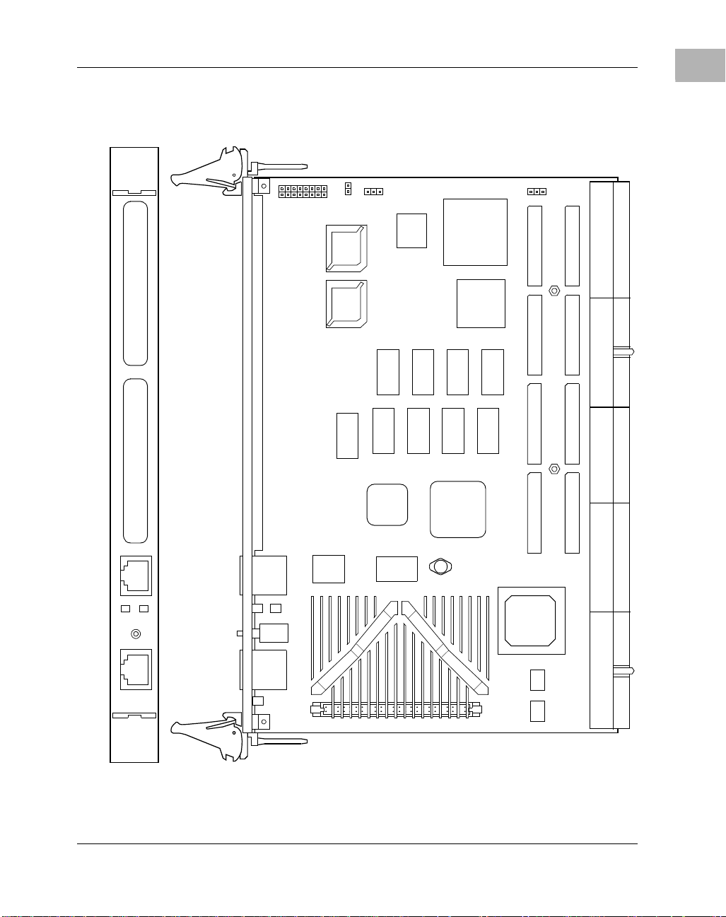
4. Carefully remove the MCPN750A from its CompactPCI card slot
and lay it flat, with connectors J1 through J5 facing you.
Page 43

!
Caution
Hardware Installation
1
Avoid touching areas of integrated circuitry; static discharge can damage
these circuits.
5. Remove the PMC filler from the front panel of the MCPN750A.
6. Slide the edge connector of the PMC module into the front panel
opening from behind and place the PMC module on top of the
baseboard. The four connectors on the underside of the PMC
module should then connect smoothly with the corresponding
connectors (J11/12/13/14) on the MCPN750A.
7. Insert the four short Phillips screws, provided with the PMC,
through the holes on the bottom side of the MCPN750A into the
PMC front bezel and rear standoffs. Tighten the screws.
8. Reinstall the MCPN750A assembly in its proper card slot. Be sure
the module is well seated in the backplane connectors. Do not
damage or bend connector pins.
9. Replace the chassis or syst em cover( s), reco nnect the sys tem to the
AC or DC power source, and turn the equipment power on.
Note If the PMC provides rear I/O, refer to Chapter 7, Connector Pin
Assignments for the pin assignments. Connectors on the
TMCPN710 and TM-PIMC-0001 provide rear panel access to
these signals.
http://www.motorola.com/computer/literature 1-23
Page 44

1
Hardware Preparation and Installation
Installing the MCPN750A Baseboard
With mezzanine board(s) installed (if applicable) and headers properly
configured, proceed as follows to install the MCPN750A in the
CompactPCI chassis:
1. Attach an ESD strap to your wri st. Att ach the o ther en d of the ESD
strap to the chassis as a ground. The ESD strap must be secured to
your wrist and to ground throughout the procedure.
2. In a non-hot swap system, perform an operating system shutdown.
Turn the AC or DC power off and remove the AC cord or DC power
lines from the system. Remove chassis or system cover(s) as
necessary for access to the CompactPCI modules.
Inserting or removing modules in a non-hot swap chassis with power
!
Caution
applied may result in damage to modul e component s. The MCPN750A is
a hot swappable board and may be inse rted in a h ot swap c hassis such as a
CPX2000, or a CPX8000 series chassis with power applied.
Dangerous voltages, capable of causing death, are present in
this equipment. Use extreme caution when handling, testing,
and adjusting.
3. Remove the filler panel from the appropriate non-system card slot.
4. Set the VIO on the backplane to either +3.3V or +5V (the
MCPN750A is a Universal board), depending upon your cPCI
system signaling requirements and ensure the backplane does not
bus J3, or J5 signals.
5. Slide the MCPN750A into the appropriate non-system slot.
Grasping the top and bottom inject or handles, be sure the module is
well seated in the P1 through P5 connectors on the backplane. Do
not damage or bend connector pins.
1-24 Computer Group Literature Center Web Site
Page 45

!
Caution
Hardware Installation
1
Avoid touching areas of integrated circuitry; static discharge can damage
these circuits
6. Secure the MCPN750A in the chassis with the screws provided,
making good contact wi th the transverse mou nting rails to minimize
RF emissions.
7. Replace the chassis or system cover(s), making sure no cables are
pinched. Cable the peripherals to the panel connectors, reconnect
the system to the AC or DC power source, and turn the equipment
power on.
http://www.motorola.com/computer/literature 1-25
Page 46

1
Hardware Preparation and Installation
Installing a TMCPN710 or TM-PIMC-0001 Transition Module
The TMCPN710 or TM-PIMC-0001 Transition Module may be required
to complete the configu ration of your particular MCPN750A system. If so,
perform the foll owi ng in stall steps to instal l th is board. For more detail ed
information on the TMCPN710 or TM-PIMC-0001 Transition Module
refer to the corresponding use rs guide, i.e., TMCPN710 Transition Mod ule
Installation and Use (TMCPN710A/ IH) or TM-PIMC-0001 Transition
Module Installation and Use (TMPIMCA/IH) manual.
Installing PIMs on the TM-PIMC-0001 Transition Module
If PIMs have already been installed on the TM-PIMC-0001, or you are
installing a transition module as it has been shipped from the factory,
disregard this section, and proceed to the main installation section titled
“Installing the Transition Module in the Chassis.” For PIM installation
perform the following steps:
1. Attach an ESD strap to your wri st. Att ach the o ther en d of the ESD
strap to the chassis as a ground. The ESD strap must be secured to
your wrist and to ground throughout the procedure.
2. Perform an operating system shutdown. Turn the AC or DC power
off and remove the AC cord or DC power lines from the system.
3. Remove chassis or system cover(s) as necessary for access to the
CompactPCI.
1-26 Computer Group Literature Center Web Site
Page 47

Hardware Installation
1
2695 0001
Figure 1-10. Installing a PIM on the TM-PIMC-0001 Transition Module
Inserting or removing modules in a non-hot swap chassis with the power
!
Caution
http://www.motorola.com/computer/literature 1-27
applied may result in damage to the module components. The TM-PIMC0001 is not a hot swap board, but it may be in stal led in a hot swap cha ssis
with power applied, if the corresponding MCPN750A is removed before
the TM-PIMC-0001 board is installed.
Page 48

1
Hardware Preparation and Installation
Dangerous voltages, capable of causing death, are present in
!
Warning
this equipment. Use extreme caution when handling, testing,
and adjusting.
4. Carefully remove the TM-PIM C -0001 from its CompactPCI card
slot and lay it flat on a stable surface.
5. Remove the PIM filler from the front panel of the TM-PIMC-0001
transition module.
6. Slide the face plate (front bezel) of the PIM module into the front
panel opening from be hind and p lace the PI M modul e on t op of the
transition module, aligned with the appropriate two PIM
connectors. The two connec tors on the underside of the PIM module
should then connect smoothly with the corresponding connectors
(J10/J14 or J20/J24) on the TM-PIMC-0001.
7. Insert the four short Phillips screws, provided with the PIM, through
the holes on t he bottom side of the TM-PIMC-000 into the PIM
front bezel and rear standoffs. Tighten the screws.
8. Reinstall the TM-PIMC-0001 assembly in its proper card slot. Be
sure the module is well seated in the backplane connectors. Do not
damage or bend connector pins.
9. Replace the chassis or syst em cover( s), reco nnect t he syste m to the
AC or DC power source, and turn the equip ment power on, or if hot
swapping, you may now install the MCPN750A.
Installing the Transition Module in the Chassis
1. Attach an ESD strap to your wri st. At tach t he oth er end of the st rap
to the chassis as a ground. The ESD strap must be secured to your
wrist and to ground throughout the procedure.
2. Perform an operating syst em shut down. Tur n the AC or DC power
off and remove the AC cord or DC power lines from the system.
Remove chassis or system cover(s) as necessary for access to the
chassis backplane.
1-28 Computer Group Literature Center Web Site
Page 49

!
Warning
!
Caution
Hardware Installation
1
Dangerous voltages, capable of causing death, are present in
this equipment. Use extreme caution when handling, testing,
and adjusting.
Avoid touching areas of integrated circuitry; static discharge can damage
these circuits.
3. With the TMCPN710 or TM-PIMC-0001 in the correct vertical
position that matches the pin positioning of the corresponding
MCPN750A board carefully slide the transition module into the
appropriate slot and sea t ti ghtl y into the backpla ne. Ref er to Figure
1-11. TMCPN710 or TM-PIMC-0001/MCPN750A Mating
Configuration for the correct board/connector orientation.
4. Secure in place with the sc rews provided, making good con tact with
the transverse mounting rails to minimize RF emissions.
5. Replace the chassis or system cover(s), making sure no cables are
pinched. Cable the peripherals to the panel connectors, reconnect
the system to the AC or DC power source, and turn the equipment
power on.
http://www.motorola.com/computer/literature 1-29
Page 50

1
Hardware Preparation and Installation
MCPN750A
P5
P4
P3
P2
P1
P5
P4
P3
TMCPN710
or
TM-PIMC-0001
Figure 1-11. TMCPN710 or TM-PIMC-0001/MCPN750A Mating Configuration
1-30 Computer Group Literature Center Web Site
Page 51

MCPN750A Module Power Requirements
MCPN750A Module Power Requirements
The MCPN750A board draws +5V, +3.3V and VIO power from the J1
connector. The +12V and - 12V voltages are moni tored by the MCPN750A
hot swap controller and provided for use by the PMCs and transition
modules. The MCPN750A contains an elect ronic circuit breaker that limits
the total +5V, +3.3V, +12V and -12V current drawn by the MCPN750A.
Refer to the table below for the electrical current available to the PMCs and
transition modules and Appendix A for other specs.
Voltage Current Available to PMCs & Transition Modules
+5.0V 6 Amps
+3.3V 6 Amps
+12.0V 1 Amp
-12.0V 0.4 Amp
1
http://www.motorola.com/computer/literature 1-31
Page 52

1
Hardware Preparation and Installation
1-32 Computer Group Literature Center Web Site
Page 53

2Startup and Operation
Introduction
This chapter supplies information for use of the MCPN750A family of
Single Board Computers in a s ystem configur ation. Here you will fi nd the
power-up procedure and descriptions of the switches and LEDs, memory
maps, and software initialization.
Applying Power
After you have verified that all necessary hardware preparation has been
done, that all connections have been made correctly, and that the
installation is complete, you can power up the system. The MPU,
hardware, and firmware initialization process is performed by the
PowerPC™ PPCBug power-up or system reset. The firmware initializes
the devices on the SBC module in preparation for booting the operating
system.
2
The firmware is shipped from the factory with an appropriate set of
defaults. In most cases the re is no need to modify the firmware
configuration before you boot the operating system.
The following flowchart shows the basic initialization process that takes
place during PowerPC system startup.
For further information on PPCBug, refer to Chapters 3 and 4 in this
manual, or to the PPCBug Firmware Package User’s Manual.
2-1
Page 54

Startup and Operation
2
STARTUP
SYSTEM
INITIALIZATION
CONSOLE
DETECTION
RUN SELFTESTS
(IF ENABLED)
AUTOBOOT
(IF ENABLED)
OPERATING
SYSTEM
1173 4. 00 9702
Figure 2-1. PPCBug System Startup
The MCPN750A front panel has one
(light-emitti ng diode) status indi cators (
ABORT/RESET switch and three LED
BFL, CPU, and HOT SWAP STATUS).
For more information on front panel operation refer to Chapter 6,
Functional Description.
2-2 Computer Group Literature Center Web Site
Page 55

Memory Maps
Memory Maps
There are three points of view for memory maps:
❏ The mapping of all resou rces as vi ewed by t he proce ssor (MPU bus
memory map)
❏ The mapping of onboard resources as viewed by PCI local bus
masters (PCI bus memory map)
❏ The mapping of onboard resources as viewed by the CompactPCI
bus.
The following sections give a general description of the MCPN750A
memory organization from the above three points of view. Detailed
memory maps can be found in t he MCPN750A CompactPCI Single Board
Computer Programmer’s Reference Guide (MCPN750A/PG).
Processor Memory Map
The processor memory map configuration is under the control of the
Raven bridge control ler ASI C and the Fal con me mory c ont roll er chip set.
The Raven and Falcon devices adjust system mapping to suit a given
application via pro grammable map de coder register s. At system powe r-up
or reset, a default processor memory map takes over.
2
Default Processor Memory Map
The default processor memory map that is valid at power-up or reset
remains in effect until rep rogrammed for specific applications. Table 2-1
defines the entire default memory map ($00000000 to $FFFFFFFF).
Table 2-1. Processor Default View of the Memory Map
Processor Address
Start End
00000000 7FFFFFFF 2GB Not Mapped
80000000 8001FFFF 128KB PCI/ISA I/O Space 1
80020000 FEF7FFFF 2GB-16MB-640KB Not Mapped
FEF80000 FEF8FFFF 64KB Falcon Registers
http://www.motorola.com/computer/literature 2-3
Size Definition Notes
Page 56

Startup and Operation
2
Table 2-1. Processor Default View of the Memory Map (Continued)
Processor Address
Start End
FEF90000 FEFEFFFF 384KB Not Mapped
FEFF0000 FEFFFFFF 64KB Raven Registers
FF000000 FFEFFFFF 15MB Not Mapped
FFF00000 FFFFFFFF 1MB ROM/Flash Bank A or Bank B 2
Notes 1. Default map for PCI/ISA I/O space. Allows software to
determine whether the system is MPC105-based or
Falcon/Raven-based by examining either the PHB Device ID
or the CPU Type register.
2. The first 1MB of ROM/Flash Bank A (soldered 4MB Flash)
appears in this range after a reset if the rom_b_rv control bit in
the Falcon’s ROM B Base/Size register is cleared. If the
rom_b_rv control bit is set, this address range maps to
ROM/Flash Bank B (socketed 1MB ROM/Flash).
For detailed processor memory maps, including suggested PREPcompatible memory maps, re fer to the MCPN750A CompactPCI Single
Board Computer Programmer’s Reference Guide (part number
MCPN750A/PG).
Size Definition Notes
PCI Local Bus Memory Map
The local PCI m emory map is the P C I memory map as viewed by the
MCPN750A base board. This is also the secondary bus side of the 21554
on the MCPN750A. This map is controlled by the Raven ASIC and the
21554 PCI-to-PCI bridge. The Raven and the 21554 PCI-to-PCI bridge
have flexible programmable map decoder registers to customize the
system for a wide range of applications.
After a reset, the Raven AS IC map decoders are in their default state.
Software must program the appropriate map decoders for a specific
environment. The 21554 bridge map decoders default state is determined
by the SROM values loaded.
2-4 Computer Group Literature Center Web Site
Page 57

Memory Maps
For detailed PCI memory maps, including suggested PREP-compatible
memory maps, refer to the MCPN750A CompactPCI Single Board
Computer Programmer’s Reference Guide (MCPN750A/PG).
CompactPCI Memo ry Map
The MCPN750A uses the 21554 non-transparent PCI-to-PCI bridge to
interface between the local PCI bus and the CompactPCI bus. The 21554
is different from traditional PCI-to-P CI bridges in that it uses address
translation instead of a flat address map between primary and secondary
PCI buses. In the MCPN750A configuration, the primary bus is the
CompactPCI bus and the secondary bus is the MCPN750A local bus.
Downstream transacti ons are those that are initiated on the primary bu s
and are forwarded to the secondary bus. Upstream transactions are those
initiated on the secondary bus and forwarded to the primary bus.
Address Decoding with the 21554
The 21554 implements multi ple base addre ss registers o n both the p rimary
and secondary interfaces that denote separate address ranges for both
downstream and upstream t ransactions. It als o has base registers f or access
to its Control and Status Register (CSR) space. Consequently, on the
primary interface (CompactPCI bus) the 21554 responds only to those
transactions which are in the address range defined by one of the base
address ranges. All other addresses are ignored. The same is true for
transactions on the secondary interface (local PCI bus).
2
The address ranges defined by the primar y base a ddress re gisters reside i n
the primary or system address map. The address ranges defined by the
secondary base address registers reside in the secondary or local address
map. Each of these a ddress maps i s independ ent of ea ch oth er. The 2155 4
provide address translation between these two address maps when
forwarding transactions upstream or downstream.
Recommendations for CompactPCI mapping, including suggested PREPcompatible memory maps, can be found in the MCPN750A CompactPCI
Single Board Computer Programmer’s Reference Guide
(MCPN750A/PG).
http://www.motorola.com/computer/literature 2-5
Page 58

Startup and Operation
2
L2 Cache
The MCPN750A SBC uses a backside L2 cache structure via the MPC750
processor chip. The MPC750 L2 cache is implemented with an onchip 2way set-associative t ag memor y and exte rnal direct-mapped synch rono us
SRAMs for data storage. The external SRAMs are accessed through a
dedicated 72-bit wide (64 bits of data and 8 bits of parity) L2 cache port.
The MPC750 will support 256KB, 512KB or 1MB of L2 cache SRAMs.
The L2 cache can operate in copyback or writethru modes and supports
system cache coherenc y through snooping. Parity generation an d checking
may be disabled by programming the MPC750 accordingly. Refer to the
MPC750 Data Sheet and the MCPN750A CompactPCI Single Board
Computer Programmer’s Reference Guide (MCPN750A/PG) for
additional information.
System Clock Generator
The system clocks f or the processor, Ra ven/Falcon chipset (66 MHz) and
each of the onboard PCI devices (33 MHz) are generated by a 66 MHz
oscillator and dist ributed by the MPC949 clock buffe r. Separate oscillators
are provided as follows: 14.31818 MHz for the PBC internal timer; 20
MHz for the ethernet MAC interface; 25 MHz for the ethernet PHY
device; 48 MHz for the USB interface; 1.843 MHz for the serial ports.
PPC Bus Arbitration
The arbitration control for the PPC bus is provided by a Programmable
Logic Device (PLD). There ar e only two potential PPC masters, Ra ven and
MPC750, with Raven having the highest priority. See the following
section titled “PCI Arbitration” for a description of arbitration control of
onboard PCI devices.
PCI Host Bridge
The Raven ASIC provides the bridge function between the PPC60X bus
and the onboard PCI Local Bus. Raven is a PCI 2.1 compliant 64-bit PCI
implementation for 32/64-bit data transfers. Dual Address Cycle is not
2-6 Computer Group Literature Center Web Site
Page 59

Memory Maps
supported. The Raven supports PowerPC processor external bus
frequencies up to 66 MHz and PCI fre quenci es up to 33 MHz. The Ra ven
is connected to the proces sor data parity si gnals to provide pro ces sor data
bus parity generation and checking.
There are four programmable map decoders for each direction to provide
flexible address mappings between the PPC/DRAM and the PCI Local
Bus. Refer to the MCPN750A CompactPCI Single Board Computer
Programmer’s Reference Guide (MCPN750A/PG) for additional
information and programming details.
2
http://www.motorola.com/computer/literature 2-7
Page 60

Startup and Operation
2
PCI Arbitration
The MCPN750A has six potential local PCI bus masters:
❏ the Raven ASIC,
❏ the PBC de vice (VT82C586B),
❏ the Ethernet device (21143),
❏ the PCI-to-PCI bridge device (21554),
❏ and each of the two PMCs.
The local PCI arbiter is implemented in an onboard PLD. This arbiter
implements a rotat ing priority sc heme with equal priorities. Sin ce the PBC
device does not support bus parking, the arbiter will park on the Raven
when the bus is idle.
Interrupt Handling
The Raven ASIC provides a Multi -Processo r Int errupt Contro ller (MPIC)
to handle various interrupt sources. This MPIC supports up to two
processors and 16 external interrupt sources. There are also six other
interrupt sourc es inside the MPIC: Two cross-processor i nterrupts and four
timer interrupts. All ISA interrupts go through the 8259 pair in the
Peripheral Bus Contr oller (PBC). The outp ut of the PBC then go es through
the MPIC in Raven.
Since the MCPN750A board is designed to support processor data bus
parity, the Raven us es some of the pins nor mally used a s external interrupt
inputs as parity pins. Therefore, an Interrupt Multiplexer device,
implemented in a PLD, is used to scan the external MPIC interrupts into
Raven as a serial bit s tream usi ng the Raven SISTA and SIDAT pi ns. This
operation is a ut omatic and transpare nt to the softwa re . A maximum delay
of 240 nanoseconds should be expected from the time that the external
interrupt is generated and when it is presented to the MPIC. Sources of
interrupts may be any of the following:
❏ The Raven ASIC itself (four MPIC t imer interr upts or tra nsfer error
interrupts)
2-8 Computer Group Literature Center Web Site
Page 61

Memory Maps
❏ The Processor 0 (processor self-interrupts)
❏ Transfer Error Interrupt (from the Raven ASIC)
❏ The Falcon chip set (memo ry error interr upts)
❏ The PCI bus (interrupts from PCI devices)
❏ The CPCI bus (interrupts from CPCI devices)
❏ Power monitor interrupts
❏ Watchdog timer interrupt
❏ The ISA bus (interrupts from ISA devices)
The ISA interrupts are handled as a single 8259 interrupt from the
VT82C586B PBC device.
For details on interrupt handling, refer to the MCPN750A CompactPCI
Single Board Computer Programmer’s Reference Guide
(MCPN750A/PG).
ISA DMA Channels
The PBC supports seven 8237 compatible DM A channels. ISA compat ible
type A, B and F timing is supported. These DMA channels are not used
since there are no ISA DMA devices.
2
Sources of Reset
The MCPN750A SBC provides reset control from various sources and
identifies the source of the reset in a software readable register. Hard or
soft resets may be generated. A hard reset is defined as a reset of all
onboard circuitry including the PowerPC hard reset and reset of all
onboard peripheral devices. A soft reset is defined as a reset of the
PowerPC. The MCPN750A SBC has seven potential sources of reset:
1. Power-on/Undervoltage Rese t.
2. Front Panel
depressed).
http://www.motorola.com/computer/literature 2-9
RESET switch (wil l generate a hard reset when
Page 62

Startup and Operation
2
backplane.
4. Watchdog timer Reset function controlled by the SGS-Thomson
MK48T559 Watchdog Timer or the Raven Watchdog Timer.
5. Software Hard Reset (PBC Port 92 Register)
6. 21554 PCI-to-PCI bridge Secondary Reset Bit
7. 21554 PCI-to-PCI bridge Chip Reset Bit.
The following table shows which de vices are a ffected by the various types
of resets. For details on using reset s, refer to the MCPN750A CompactPCI
Single Board Computer Programmer’s Reference Guide (part number
MCPN750A/PG).
Table 2-2. Classes of Reset and Effectiveness
3. CompactPCI Push Button Reset (RST#) from the CompactPCI
Device Affected
Reset Source
Power-On/undervoltage
Front Panel Reset switch
CompactPCI PRST#
Processor
√√√√√ √
√√√√√ √
√√√√√ √
Raven
ASIC
Falcon
Chip Set
21554
Bridge
ISA
Devices
Other PCI
Devices
Watchdog Timer reset
S/W Hard Reset (PBC
Port 92 Register)
CompactPCI Reset*
(21554 Secondary Bi t)
CompactPCI Reset**
(21554 Chip Reset Bit)
√√√√√ √
√√√ √ √
√√√#√ √
√√√√√ √
# 21554 Secondary Reset Bit does not reset the 21554 register state but
does reset the 21554 data buffers.
* A configuration write is required to clear the Secondary Reset Bit after
it has been written so this bit must not be set by the local MCPN750A
processor or else the board will lock up.
2-10 Computer Group Literature Center Web Site
Page 63

Memory Maps
** If the Chip Reset Bit is set to a 1, the bit w ill clear itself after the chip
reset is complete.
Power-On Reset
The MCPN750A SBC generates a hard reset at power-on. During power
up, reset is maintain ed for 140 to 5 60 mill iseconds a fter the vol tages have
reached the minimum threshold.
Undervoltage Reset
The MCPN750A SBC generates a hard reset when the Hot Swap power
control chip (LTC1643) detects a supply voltage +5V, +3.3V, +12V or 12V fall below mini mum thresholds of +4.75V, +3.135 V, +10.8 and -10. 8
volts respectivel y. The reset is maintained for 140 to 560 milliseconds after
the voltages have returned to the minimum threshold. For undervoltage,
the Vcc threshold to reset delay is typically 10 microseconds.
Front Panel Push Button Reset
The front panel RESET switch generates a hard reset when depressed for
more than three (3) seconds. The reset is maintained as long as the switch
is depressed.
2
CompactPCI Reset (RST#)
The CompactPCI reset s ignal RST# is mon itored by the 21 554 PCI-to-PCI
bridge chip as the primary bus reset input. The bridge will generate a
secondary bus reset that is used to generate a bo ard hard reset.
Watchdog Timer Re set
Both the Raven ASIC Watchdog Timer 2 and the M48T559 watchdog
timer may generate a hard reset when the associated timer expires, if this
function is enabled.
http://www.motorola.com/computer/literature 2-11
Page 64

Startup and Operation
2
Software Resets
The software is able to generate a 200 millisecond hard reset by
programming the PBC Port92 register or a soft reset by writing to the
Processor Init Registe r of the Raven MPIC. Note that the Por t 92 reset will
reset every device o n the bo ard exc ept t he 21554 b ridge chip. Ref er t o the
MCPN750A CompactPCI Single Board Computer Programmer’s
Reference Guide (MCPN750A/PG) fo r register d etails. A board har d reset
may also be generated by writing to the 21554 Bridge Control register
from the PCI address space. This allows t he System Slot processo r to do a
software controll ed reset of the MCPN750A SBC. Refer t o the Intel 21554
Data Sheet for details .
Reset Source Identification
The source of any hard reset can be identified following the reset by
reading the Reset Source register. Refer to the MCPN750A CompactPCI
Single Board Computer Programmer’s Reference Guide
(MCPN750A/PG) for bi t assignmen ts.
Endian Issues
The MCPN750A supports b oth lit tle-endian and big- endian s oftware. The
PowerPC is inherently big-endian, while the PCI bus is inh erently littl eendian. The following sections summarize how the MCPN750A handles
software and hardware differences in big- and little-endian operations. For
further details on endian considerations, refer to the MCPN750A
CompactPCI Single Board Computer Programmer’s Reference Guide
(MCPN750A/PG).
Processor/Memory Domain
The MPC750 processor can operate in both big-endian and little-endian
mode. However, it always treat s the external processor/ memory bus as bigendian by performing address rearrangement and reordering when
running in little-endian mode. The PPC registers in the Raven PCI bus
bridge controller ASIC an d the Falcon memory cont roller chip set , as well
as DRAM, ROM/Flash, and system regist ers, always appear as big-endian.
2-12 Computer Group Literature Center Web Site
Page 65

Memory Maps
PCI Domain
Role of the Raven ASIC
2
Because the PCI bus is litt le-endian, the Raven performs byte swap ping in
both directions (from PCI to memory and from the processor to PCI) to
maintain address invariance while programmed to operate in big-endian
mode with the processor and the memory subsystem.
In little-endian mode, the Raven reverse-rearranges the address for PCIbound accesses and rearranges the address for memory-bound accesses
(from PCI). In this case, no byte swapping is done.
The PCI bus is inherently little-endian. All devices connected directly to
the PCI bus operate in little-endian mode, regardless of the mode of
operation in the processor’s domain.
PCI and Ethernet
Ethernet is also byte-stream-oriented; the byte having the lowest address
in memory is t he firs t one to b e t ransf erre d rega rd less of th e endian mode.
Since the Raven maintains add ress invariance in bot h little-endian an d bigendian mode, no endian issues should arise for Ethernet data. Big-endian
software must still take the byte-swapping effect into account when
accessing the registers of the PCI/Ethernet device, however.
http://www.motorola.com/computer/literature 2-13
Page 66

Startup and Operation
2
2-14 Computer Group Literature Center Web Site
Page 67

PPCBug Overview
The PPCBug firmware is the layer of software just above the h ardware.
The firmware provides the proper initialization for the devices on the
MCPN750A motherboard upon power-up or reset.
This chapter describes the basics of PPCBug and its architecture. It also
describes the monitor (interactive command portion of the firmware) in
detail, and gives information on act ual ly us ing the PPCBug debugger and
the special commands. A complete list of PPCBug commands appears at
the end of the chapter.
Chapter 6 contains information about the CNFG and ENV commands,
system calls, and other advanced user topics.
For full user information about PPCbug, refer to the PPCBug Firmware
Package User’s Manual and the PPCBug Diagnostics Manual, listed in
the Related Documentation appendix.
3PPCBug
3
PPCBug Basics
The PowerPC debug firmware, PPCBug, is a powerful evaluation and
debugging tool for systems built around the Motorola PowerPC
microcomputers. Facilities are available for loading and executing user
programs under complete operator control for system evaluation.
PPCBug provides a high degree of functionality, user friendliness,
portability, and ease of maintenance.
It is portable and easy to understand because it was written entirely in the
C programming language, except where necessary to use assembler
functions.
PPCBug includes commands for:
❏ Display and modification of memory
3-1
Page 68

PPCBug
❏ Breakpoint and tracing capabilities
❏ A powerful assembler and disassembler useful for patching
programs
3
❏ A self-test at power-up feature which verifies the integrity of the
system
PPCBug consists of three parts:
❏ A command-driven, user-interactive software debugger, described
in the PPCBug Firmware Package User’s Manual. It is hereafter
referred to as “the debugger” or “PPCBug”.
❏ A command-driven diagnostics package for the MCPN750A
hardware, hereafter referred to as “the diagnostics.” The diagn ostics
package is described in the PPCBug Diagnostics Manual.
❏ A user interface or debug/diagnostics monitor that accepts
commands from the system console terminal.
When using PPCBug, you operate out of e it her the debugger directory or
the diagnostic directory.
❏ If you are in the debugger directory, the debugger prompt PPC1-
Bug> is displayed and you have all of the debugger commands at
your disposal.
❏ If you are in the diagnostic directory, the diagnostic prompt PPC1-
Diag>
is displayed a nd you have all of the diagn ostic comma nds a t
your disposal as well as all of the debugger commands.
Use the SD command to switch back and forth between these directories.
Because PPCBug is command-driv en, it performs it s various operatio ns in
response to user commands entered at the keyboard. When you enter a
command, PPCBug executes the command and the prompt reappears.
However, if you enter a command that causes executi on of user target code
(e.g., GO), then control may or may not return to PPCBug, de pend ing on
the outcome of the user program.
3-2 Computer Group Literature Center Web Site
Page 69

Memory Requirements
PPCBug requires a maximum of 768KB of read/write memory (i.e.,
DRAM). The debugger allocates this space from the top of memory. For
example, a system containing 64MB ($04000000) of read/write memory
will place the PPCBug memory page at locations $03F80000 to
$03FFFFFF.
PPCBug Implementation
PPCBug is written largely in the C programming language, providing
benefits of portability and maintainability. Where necessary, assembly
language has been used in the form of separately compiled program
modules containing only as sembler code. No mixed-lang uage modules are
used.
Physically, PPCBug is contained in two socketed 32-pin PLCC Flash
devices that together provide 1MB of storage. The executable code is
checksummed at every power-on or reset firmware entry, and the result
(which includes a preca lculated checks um contained in the Fla sh devices),
is verified against the expected checksum.
MPU, Hardware, and Firmware Initialization
3
MPU, Hardware, and Firmware Initialization
The debugger performs the MPU, hardware, and firmware initialization
process. This process occu rs each time the MCPN750A is reset or power ed
up. The steps below are a high-level outline; not all of the detailed steps
are listed.
1. Sets MPU.MSR to known value.
2. Invalidates the MPU’s data/instruction caches.
3. Clears all segment registers of the MPU.
4. Clears all block address translation registers of the MPU.
5. Initializes the MPU-bus-to-PCI-bus bridge device.
6. Initializes the PCI-bus-to-ISA-bus bridge device.
http://www.motorola.com/computer/literature 3-3
Page 70

PPCBug
7. Calculate the external bus clock speed of the MPU.
8. Delays for 750 milliseconds.
3
9. Determines the CPU board type.
10. Sizes the local read/write memory (i.e., DRAM).
11. Initializes the read/write memory contr oller.
12. Sets base address of memory to $00000000.
13. Retrieve s the speed of read/write memory .
14. Initializes the read/write memory contr oller with the spe ed of
read/write memory .
15. Retrie ves the speed of read only memory (i.e., Flash) from
NVRAM.
16. Initializes the read only memory controller with the speed of read
only memory .
17. Enables the MPU’s instruction cache.
18. Copies the MPU’s exception vector table from $FFF00000 to
$00000000.
19. Verifies MPU type.
20. Enable the super-scalar feature of the MPU (boards with MPC750
type chips only).
21. Determines the debugger’s console/host ports, and initializes the
appropriate devices (PC16550/GD54xx/Z85C230).
22. Displays the debugger’s copyright message.
23. Displays any hardware i nitialization e rrors that may ha ve occurred.
24. Checksums the debugger obj ect, and di splays a war ning messag e if
the checksum failed to verify.
25. Displays the amount of local read/write memory found.
3-4 Computer Group Literature Center Web Site
Page 71

Using PPCBug
26. Verifies the configuration data that is resident in NVRAM, and
displays a warning message if the verification failed.
27. Calculates and displ ays the MPU clock spee d, verifies that the MPU
clock speed matches the configura tion data , and displ ays a warni ng
message if the verificatio n fails.
28. Displays the BUS clock speed, verifies that the BUS clock speed
matches the configuration data, and displays a warning message if
the verification fails.
29. Probes PCI bus for supported network devices.
30. Probes PCI bus for supported mass storage devices.
31. Initializes the memory/IO addresses for the supported PCI bus
devices.
32. Executes Self-Test, if so configured. (Default is no Self-Test.)
33. Extinguishes the boa rd fai l LED, if there are no se lf -test failures or
initialization/configuration errors.
3
34. Executes the configured boot routine, either ROMboot, Autoboot,
or Network Autoboot.
35. Executes the user interface (i.e., displays the
PPC1-Diag>
prompt).
PPC1-Bug> or
Using PPCBug
PPCBug is command-driven; it pe rforms its various operatio ns in response
to commands that you enter at the keyboard. When the
appears on the screen, the debugger is ready to accept debugger
commands. When the
debugger is ready to accept diagnostic commands. To switch from one
mode to the other, enter SD.
http://www.motorola.com/computer/literature 3-5
PPC1-Diag prompt appears on the screen, the
PPC1-Bug prompt
Page 72

PPCBug
What you key in is stored in an internal buff er. Execution begi ns only after
you press the Return or Ent er key . This al lows you t o co rrect ent ry err ors,
if necessary, with the control characters described in the PPCBug
3
Firmware Package User’s Manual, Chapter 2.
After the debugger executes the command, the prompt reappears.
However, if the command causes execution of user target code (for
example GO) then control may or may not return to the debugger,
depending on what the user progra m does. For example, if a breakpoint has
been specified, t hen control retu rns to the debugger when the breakp oint is
encountered during execution of the user program. Alternately, the user
program could return to the deb ugger by means of the System Call Handler
routine RETURN (described in the PPCBug Firmware Package User’s
Manual, Chapter 5). For mo re about this , refer to the GD, GO, and GT
command descriptions in the PPCBug Firmware Packa ge User’s Manual ,
Chapter 3.
A debugger command is made up of the following parts:
❏ The command name, either uppercase or lowercase (e.g., MD or
md).
❏ Any required arguments, as specified by command.
❏ At least one space before the first argument. Precede all other
arguments with either a space or comma.
❏ One or more options. Precede an option or a string of options with
a semicolon (;). If no option is entered, the command’s default
option conditions are used.
Debugger Commands
The individual debugger commands are listed in the following table. The
commands are described in detail in the PPCBug Firmware Package
User’s Manual, Chapter 2
Note You can list all the available debugger commands by entering the
Help (
HE) command alone. You can view the syntax (description)
for a particular command by entering HE followed by a space,
3-6 Computer Group Literature Center Web Site
.
Page 73

Using PPCBug
followed by the particular command mnemonic
followed by a carriage return. Keep in mind that help is now
available on both the BUG and DIAG side. In addition, issuing help
on a DIAG test category will give more informa tion about the tests
in that category. The later is accomplished by entering HE,
followed by a space, followed by the test category description (e.g.,
UART), followed by a carriage return.
Table 3-1. Debugger Commands
Command Description
AS One Line Assembler
BC Block of Memory Compare
BF Block of Memory Fill
BI Blo c k of Memory Initialize
BM Block of Memory Move
BR Breakpoint Insert
NOBR Brea kpoint Delete
BS Block of Memory Search
BV Block of Memory Verify
CACHE Disable/Enable Cache
CM Concurrent Mode
NOCM No Concurrent Mode
CNFG Configure Board Information Block
CS Checksum
CSAR PCI Configuration Space READ Access
CSAW PCI Configuration Space WRITE Access
DC Data Conversion
DMA Block of Memory Move
DS One Line Disassembler
DU Dump S-Records
ECHO Echo String
ENV Set Environment
FORK Fork Idle MPU at Address
, as listed below,
3
http://www.motorola.com/computer/literature 3-7
Page 74

PPCBug
Table 3-1. Debugger Commands (Continued)
Command Description
3
FORKWR Fork Idle MPU with Registers
GD Go Direct (Ignore Breakpoints)
GEVBOOT Global Environment Variable Boot
GEVDEL Global Environment Variable Delete
GEVDUMP Global Environment Variable(s) Dump
GEVEDIT Global Environm ent Variable Edit
GEVINIT Global Environment Variable Initialization
GEVSHOW Global Environment Variable(s) Display
GN Go to Next Instruction
GO Go Execute User Program
GT Go to Temporary Breakpoint
HE Help
IDLE Idle Master MPU
IOC I/O Control for Disk
IOI I/O Inquiry
IOP I/O Physical (Direct Disk Access)
IOT I/O Teach for Configuring Disk Controller
IRD Idle MPU Register Display
IRM Idle MPU Register Modify
IRS Idle MPU Register Set
LO Load S-Records from Host
MA Macro Define/Display
NOMA Macro Delete
MAE Macro Edit
MAL Enable Macro Listing
NOMAL Disable Macro Listing
MAR Load Macros
MAW Save Macros
MD, MDS Memory Display
3-8 Computer Group Literature Center Web Site
Page 75

Table 3-1. Debugger Commands (Continued)
Command Description
MENU System Menu
MM Memory Modify
MMD Memory Map Diagnostic
MS Memory Set
MW Memory Write
NAB Automatic Network Boot
NAP N ap MPU
NBH Network Boot Operating System, Halt
NBO Network Boot Operating System
NIOC Network I/O Control
NIOP Network I/O Physical
NIOT Network I/O Teach (Configuration)
NPING Network Ping
OF Offset Registers Display/Modify
PA Printer Attach
NOPA Printer Detach
PBOOT Bootstrap Operating System
PF Port Format
NOPF Port Detach
PFLASH Program FLASH Memory
PS Put RTC into Power Save Mode
RB ROMboot Enable
NORB ROMboot Disable
RD Register Display
REMOTE Remote
RESET Cold/Warm Reset
RL Read Loop
RM Register Modify
RS Register Set
Using PPCBug
3
http://www.motorola.com/computer/literature 3-9
Page 76

PPCBug
Table 3-1. Debugger Commands (Continued)
Command Description
3
RUN MPU Execution/Status
SD Switch Directories
SET Set Time and Date
SROM SROM Examine /Modify
SYM Symbol Table Attach
NOSYM Symbol Table Detach
SYMS Symbol Table Display/Search
T Trace
TA Terminal Attach
TIME Display Time and Date
TM Transparent Mode
TT Trace to Temporary Breakpoint
VE Verify S-Records Against Memory
VER Revision/Vers ion Display
WL Write Loop
Although a command to allow the erasing and reprogramming of Flash
!
Caution
memory is available t o you, kee p in mind that reprogr amming any po rtion
of the MCPN750A baseboard’s Flash memory (Bank B) will erase
everything currently contained in the baseboard Flash, including the
PPCBug debugger.
Diagnostic Tests
The PPCBug hardware diagnostics are intended for testing and
troubleshooting the MCPN750A module.
In order to use the diagno stics, you must switch to the di agnostic directory.
You may switch betw een dire ctories b y using the SD (Switch Dir ectories)
command. You may view a list of the commands in the di recto ry that you
are currently in by using the HE (Help) command.
3-10 Computer Group Literature Center Web Site
Page 77

Using PPCBug
If you are in the debugger directory, the debugger prompt PPC1-Bug>
displays, and all of the debugger commands are available. Diagnostics
commands cannot be entered at the
PPC1-Bug> prompt.
If you are in the diagnostic directory, the diagnostic prompt
PPC1-Diag>
displays, and all of the debugger and diagnostic commands are available.
Note that not all tests are valid for the MCPN750A. Usin g the HE
command, you can list the diagnost ic routine s available in each t est group.
Refer to the PPCBug Diagnostics Manual for complete descriptions of the
diagnostic routines and instructions on how to invoke them.
Table 3-2. Diagnostic Test Groups
Test Set Description
CL1283 Parallel Interface (CL1283)
DEC DECchip 21x4x EIDE Tests
ISABRDGE PCI/ISA Bridge Tests
KBD8730x PC8730x Keyboard/Mouse Tests*
L2CACHE Level 2 Cache Tests
NCR NCR 53C8xx SCSI-2 I/O Processor Tests*
PAR8730x PC8730x Parallel Port Test*
PCIBUS Generic PCI/PMC Slot Test
RAM Random Access Memory Tests
RTC MK48Txx Real-Time Clock Tests
SCC Serial Communications Controller Tests
UART Serial Input/Output UART Tests
VGA543x Video Graphics Tests*
Z8536 Zilog Z8536 Counter/Timer Tests*
3
http://www.motorola.com/computer/literature 3-11
Page 78

PPCBug
Notes You may enter command names in either uppercase or
lowercase.
Some diagnostics depend on restart defaults that are set up
3
only in a particular rest art mode. Refer to the documentation
on a particular diagnostic for the correct mode.
Test Sets marked with an asterisk (*) are not available on the
MCPN750A, unless SCSI or Video PMCs are installed.
3-12 Computer Group Literature Center Web Site
Page 79

4CNFG and ENV Commands
Overview
You can use the factory-installed debug monitor, PPCBug, to modify
certain parameters contained in the PowerPC board’s Non-Volatile RAM
(NVRAM), also known as Battery Backed-up RAM (BBRAM).
The CNFG and ENV commands are both described in the PPCBug
Firmware Package User’s Manual (part number PPCBUGA1/UM). Refer
to that manual for general information about their use and capabilities.
The following para graphs present additi onal information abou t CNFG and
ENV that is specific to the PPCBug debugger, along with the parameters
that can be configured with the ENV command.
4
❏ The Board Information Block in NVRAM contains various
elements concerning operati ng parame ters of the ha rdware. Use the
PPCBug command CNFG to change those parameters.
❏ Use the PPCBug command ENV to change configured PPCBug
parameters in NVRAM.
4-1
Page 80

CNFG and ENV Commands
CNFG - Configure Board Information Block
Use this command to displa y and config ure the Board I nformat ion Bloc k,
which is stored in the NVRAM. The Board Inf ormation Block lists details
of your specific board, such as the Board Serial Number, the Board
Identifier, the Bus Clock Speed, and other operational or ID
4
characteristics. The example below displays a typical Board Information
Block:
Board (PWA) Serial Number = “2717994 ”
Board Identifier = “MCPN750-60X-
0XX
Artwork (PWA) Identifier = “01-w3611F01B ”
MPU Clock Speed = “233 ”
Bus Clock Speed = “067 ”
Ethernet Address = $0001AFxxxxx
Local SCSI Identifier* = “07”
System Serial Number = “1234567 ”
”
System Identifier = “Motorola MCPN750603-
001a”
License Identifier = “12345678 “
The value or identifier to the right of the equal sign is displayed as leftjustified character (ASCII) strings padded with space characters, and
quotes (“) are displayed to indicate the size of the string. Values that are
not in quotes are considered data strings, and data strings are rightjustified. The data strings are padded with zeroes if the length is not met.
*Note: the MCPN750A has no local SCSI bus controlle r, hence, the Local
SCSI Identifier parameter is ignored by the PPCBug.
The Board Information Block is factory-configured before shipment.
There is no need to modify block parameters unless the NVRAM is
corrupted. Refer to the MCPN750A Compac tPCI Single Board Computer
Programmer’s Reference Guide (MCPN750A/PG) for the actua l locat ion
and other information about the Board Information Block. Refer to the
PPCBug Firmware Package User's Manual (PPCBUGA1/UM) for a
description of CNFG and examples.
4-2 Computer Group Literature Center Web Site
Page 81

ENV - Set Environment
Use the ENV command to vi ew and/or confi gure interactiv ely all PPCBug
operational parameters that are kept in Non-Volatile RAM (NVRAM).
Refer to the PPCBug Firmware Package User’s Manual
(PPCBUGA1/UM) for a description of the use of ENV.
Listed and described below are the parameters that you can configure
using ENV. The default values shown were those in effect when this
publication went to print.
Configuring the PPCBug Parameters
The parameters that can be configured using ENV are:
Bug or System environment [B/S] = B?
ENV - Set Environment
4
B
S
Field Service Menu Enable [Y/N] = N?
Y
N
Probe System for Supported I/O Controllers [Y/N] = Y?
Y
N
Bug is the mode where no system type of support is
displayed. However, system-related items are still
available. (Default)
System is the standard mode of operation, and is the
default mode if NVRAM should fail. System mode is
defined in the PPCBug Firmware Package User’s
Manual.
Display the field service menu.
Do not display the field service menu. (Default)
Accesses will be made to the appropriate system
buses (e.g., VMEbus, local MPU bus) to determine
the presence of supported controllers. (Default)
Accesses will not be made to the VMEbus to
determine the presence of supported controllers.
http://www.motorola.com/computer/literature 4-3
Page 82

CNFG and ENV Commands
Auto-Initialize of NVRAM Header Enable [Y/N] = Y?
Y
NVRAM (PReP partition) header space will be
initialized automatically during board initialization,
but only if the PReP partition fails a sanity check.
(Default)
4
Network PReP-Boot Mode Enable [Y/N] = N?
N
Y
NVRAM header space will not be initialized
automatically during board initialization.
Enable PReP-style network booting (same boot image
from a network interface as from a mass storage
device).
N
SCSI Bus Reset on Debugger Startup [Y/N] = N?
Y
N
Primary SCSI Bus Negotiations Type [A/S/N] = A?
A
S
Do not enable PReP-style network booting. (Default)
SCSI bus is reset on debugger setup.
SCSI bus is not reset on debugger setup. (Default)
Asynchronous SCSI bus negotiation. (Default)
Synchronous SCSI bus negotiation.
N
Primary SCSI Data Bus Width [W/N] = N?
W
N
Secondary SCSI Identifier = “07”?
None.
Wide SCSI (16-bit bus).
Narrow SCSI (8-bit bus). (Default)
If the board has a s econdary SCSI contro ller, th is number i s the se condary
SCSI ID or address. For the MCPN750A, all PCI add-on SCSI
controllers/adapters supported by PPCBug are set to the SCSI ID value
entered here.
4-4 Computer Group Literature Center Web Site
Page 83

ENV - Set Environment
NVRAM Bootlist (GEV.fw-boot-path) Boot Enable [Y/N] = N?
Y
Give boot priority to devices defined in the fw-bootpath globa l environment va riable (GEV).
N
Do not give boot priority to devices listed in the fwboot-path GEV. (D efault)
Note When enabled, the GEV (Global Environment Variable) boot
takes priority over all other boots, including Autoboot and
Network Boot.
NVRAM Bootlist (GEV.fw-boot-path) Boot at power-up only [Y/N] = N?
Y
Give boot priority to devices defined in the fw-bootpath GEV at power-up reset only.
N
Give power-up boot priority to devices list e d in the
fw-boot-path GEV at any reset. (Default)
NVRAM Bootlist (GEV.fw-boot-path) Boot Abort Delay = 5?
The time in seconds that a boot fr om the NVRAM boot list wi ll del ay
before starting the boot . The pu rpose for the delay is to a llo w you t he
option of stopping the boot by use of the
BREAK key. The time value
is from 0-255 seconds. (Default = 5 seconds)
Auto Boot Enable [Y/N] = N?
4
Y
N
Auto Boot at power-up only [Y/N] = N?
Y
N
The Autoboot function is enabled.
The Autoboot function is disabled. (Default)
Autoboot is attempted at power-up reset only.
Autoboot is attempted at any reset. (Default)
http://www.motorola.com/computer/literature 4-5
Page 84

CNFG and ENV Commands
Auto Boot Scan Enable [Y/N] = Y?
Y
N
4
Auto Boot Scan Device Type List = FDISK/CDROM/TAPE/HDISK?
If Autoboot is enabled, th e Autoboot process attem pts
to boot from devices specified in the scan list (e.g.,
FDISK/CDROM/TAPE/HDISK). (Default)
If Autoboot is enabled, the Autoboot process uses the
Controller LUN and Device LUN to boot.
This is the listing of boot devices displayed if the Autoboot Scan
option is enabled. If you modify the list, follow the format shown
above (uppercase letters, using forward slash as separator).
Auto Boot Controller LUN = 00?
Refer to the PPCBug Firmware Package User’s Manual for a listing
of disk/tape controller modules currently supported by PPCBug.
(Default = $00)
Auto Boot Device LUN = 00?
Refer to the PPCBug Firmware Package User’s Manual for a listing
of disk/tape devices currently supported by PPCBug.
(Default = $00)
Auto Boot Partition Number = 00?
Which disk “partition” is to be booted, as specified in the PowerPC
Reference Platform (PRP) specification. If set to zero, the firmware
will search the partitions in order (1, 2, 3, 4) until it finds the first
“bootable” partition. That is then the partition that will be booted.
Other acceptable values are 1, 2, 3, or 4. In these four cases, the
partition specified will be booted without searching.
Auto Boot Abort Delay = 7?
The time in seconds that the Autoboot sequence will delay before
starting the boot. The pu rpo se f or the delay is to allow you the option
of stopping the boot by use of the
BREAK key. The time valu e is from
0-255 seconds. (Default = 7 seconds)
Auto Boot Default String [NULL for an empty string] =?
4-6 Computer Group Literature Center Web Site
Page 85

ENV - Set Environment
You may specify a string (filename) which is passed on to the code
being booted. The maximum length of this string is 16 characters.
(Default = null string)
ROM Boot Enable [Y/N] = N?
Y
N
ROM Boot at power-up only [Y/N] = Y?
Y
N
ROM Boot Abort Delay = 5?
The ROMboot function is enabled.
The ROMboot function is disabled. (Default)
ROMboot is attempted at power-up only. (Default)
ROMboot is attempted at any reset.
The time in seconds that the ROMboot sequence will delay before
starting the boot. The pu rpo se f or t he de la y is to allow you the option
of stopping the boot by use of the
BREAK key. The time valu e is from
0-255 seconds. (Default = 5 seconds)
ROM Boot Direct Starting Address = FFF00000?
The first location tested when PPCBug searches for a ROMboot
module. (Default = $FFF00000)
ROM Boot Direct Ending Address = FFFFFFFC?
The last location tested when PPCBug searches for a ROMboot
module. (Default = $FFFFFFFC)
4
Network Auto Boot Enable [Y/N] = N?
Y
The Network Auto Boot (NETboot) function is
enabled.
N
Network Auto Boot at power-up only [Y/N] = N?
Y
N
The NETboot function is disabled. (Default)
NETboot is attempted at power-up reset only.
NETboot is attempted at any reset. (Default)
http://www.motorola.com/computer/literature 4-7
Page 86

CNFG and ENV Commands
Network Auto Boot Controller LUN = 00?
Refer to the PPCBug Firmware Package User’s Manual for a listing
of network controller modules currently supported by PPCBug.
(Default = $00)
Network Auto Boot Device LUN = 00?
4
Refer to the PPCBug Firmware Package User’s Manual for a listing
of network controller modules currently supported by PPCBug.
(Default = $00)
Network Auto Boot Abort Delay = 5?
The time in seconds that the NETboot sequence will delay before
starting the boot. The pu rpo se f or the delay is to allow you the option
of stopping the boot by use of the
BREAK key. The time valu e is from
0-255 seconds. (Default = 5 seconds)
Network Auto Boot Configuration Parameters Offset (NVRAM) =
00001000?
The address where the net work interf ace configur ation parameters are
to be saved/retained in NVRAM; these parameters are the necessary
parameters to perform an unattended network boot. A typical offset
might be $1000, but this value is application-specific. (Default =
$00001000)
If you use the NIOT debugger command, thes e parameters need
!
Caution
to be saved somewhere in the offset range $00001000 through
$000016F7. The NIOT parameters do not exceed 128 bytes in
size. The setting of this ENV pointer determines their location.
If you have used the same space for your own program
information or commands, they will be overwritten and lost.
You can relocate the network interface configuration parameters
in this space b y using the ENV command to change the Network
Auto Boot Configuration Parameters Offset from its default of
$00001000 to the value you need to be clear of your data within
NVRAM.
4-8 Computer Group Literature Center Web Site
Page 87

Memory Size Enable [Y/N] = Y?
ENV - Set Environment
Y
N
Memory Size Starting Address = 00000000?
Memory will be sized for Self Test diagnostics.
(Default)
Memory will not be sized for Self Test diagnostics.
The default Starting Address is $00000000.
Memory Size Ending Address = 02000000?
The default Ending Address is the calculated size of loc al memor y. If
the memory start is cha nged from $00000000, this value will also need
to be adjusted.
DRAM Speed in NANO Seconds = 60?
The default setting fo r this parameter will vary depending on the speed
of the DRAM memory parts installed on the board. The default is set
to the slowest speed found on the available banks of DRAM memory.
ROM First Access Length (0 - 31) = 10?
This is the value programmed into the MPC105 “ROMFAL” field
(Memory Control Configurat ion Register 8: bits 23-27 ) to indicate the
number of clock cycles used in accessing the ROM. The lowest
allowable ROMFAL setting is $00; the highest allowable is $1F. The
value to enter depends on processor speed; refer to your specific
processor and memory mezzanine module user’s manual for
appropriate values. The de fau lt val ues va ry according to the system’s
bus clock speed.
4
Note ROM First Access Len gth is not applicable t o the MCPN750.
The configured value is ignored by PPCBug.
ROM Next Access Length (0 - 15) = 0?
The value programmed into the MPC105 “ROMNAL” field (Memory
Control Configuration Register 8: bits 28-31) to represent wait states
in access time for nibble (or burst) mode ROM accesses. The lowest
http://www.motorola.com/computer/literature 4-9
Page 88

CNFG and ENV Commands
allowable ROMNAL setting is $0; the highest allowable is $F. The
value to enter depends on processor speed; refer to your
Processor/ Memory Mezzan ine Module User’s Manual for appropriate
values. The default value varies according to the system’s bus clock
speed.
4
Note ROM Next Access Length is not applicable to the MCPN750.
The configured value is ignored by PPCBug.
DRAM Parity Enable [On-Detection/Always/Never - O/A/N] = O?
O
A
N
Note This parameter (above) also applies to enabling ECC for DRAM.
L2 Cache Parity Enable [On-Detection/Always/Never - O/A/N] = O?
O
A
N
PCI Interrupts Route Control Registers (PIRQ0/1/2/3) = 0A050900?
DRAM parity is enabled upon detection. (Default)
DRAM parity is always enabled.
DRAM parity is never enabled
L2 Cache parity is enabled upon detection. (Default)
L2 Cache parity is always enabled.
L2 Cache parity is never enabled
Initializes the PIRQx (PCI Interrupts) route con trol registers in the
IBC (PCI/ISA bus bridge controller). The ENV parameter is a 32-bit
value that is divi ded by 4 to yield t he values for rout e control registers
PIRQ0/1/2/3. The defaul t is deter mined by sy stem type. For details o n
PCI/ISA interrupt assignments and for suggested values to enter for
this parameter, refer to the 8259 Interrupts sec tion of Chapter 4 in t he
MCPN750A CompactPCI Single Board Computer Programmer’s
Reference Guide.
Serial Startup Code Master Enable [Y/N]=N?
4-10 Computer Group Literature Center Web Site
Page 89

ENV - Set Environment
The Serial Startup Codes can be displayed at key points in the
initialization of the hardware devices. Should the debugger fail to
come up to a prompt, the last code di splaye d will i ndica te how fa r the
initialization sequence had progressed before stalling. The codes are
enabled by an ENV parameter.
Serial Startup Code LF Enable [Y/N]= N?
A line feed can be inserted after each code is displayed to prevent it
from being overwritten by the next code. This is also enabled by an
ENV parameter.
A list of LED/serial codes is included in the section on MPU,
Hardware, and Firmware Initializa tion in Chapter 1 of the PPCBug
Firmware Package User’s Manual, Part 1.
A means to execute user selectable Bug commands upon Bug startup has
been added to the ENV parameters. The usage is as follows:
Firmware Command Buffer Enable [Y/N] = N?
Y - Enables the Firmware Command Buffer execution
4
N - Disables the Firmware Command Buff er execution (Default)
Firmware Command Buffer Delay = 5?
Defines the number of seconds to wait before firmware begins
executing the startup commands in the startup command buffer.
During this delay, you may press any key to prevent the execution of
the startup command buffer.
The default value of this parameter causes a startup delay of 5
seconds.
http://www.motorola.com/computer/literature 4-11
Page 90

CNFG and ENV Commands
Firmware Command Buffer
[‘NULL’ terminates entry]?
The Firmware Command Buffer content s contain the BUG commands
which are executed upon firmware startup. BUG commands you will
place into the command buffer should be typed just as you enter the
commands from the comma nd l ine . The st ri ng ‘NULL’ on a new line
4
terminates the command line entries. All BUG commands except for
the following may be used within the command buffer: DU, ECHO,
LO, TA, VE.
Note Interactive editing of the startup command buffer is not
supported. If changes are needed to an existing set of startup
commands, a new set of commands with changes must be
reentered.
4-12 Computer Group Literature Center Web Site
Page 91

5Remote Start Via the PCI Bus
Introduction
This chapter describes the remote interface provided by the firmware to the
host CPU via the cPCI bus. This interface facili tates the host obtaining
information about th e board, downloading code and/or data, and execution
of the downloaded program.
Note Application s may also be downloaded to the MCPN750A via one
of the PCI bus windows provid ed by the PCI-to -PCI bridge. Thi s
method is faster than us ing the PPCBug remote interfac e and may
be preferable to use for large downloads.
Overview
PPCBug uses one of the scratch pad registers of the 2155x PCI-to-PCI
bridge as the command/response channel. This scratch pad register is
logically divided into 5 sections:
5
❏ An ownership flag. When set, indicates that the host ‘owns’ the
register and is fr ee to write a new c ommand int o it. I t al so indi cate s
that the previous command, if any, has been completed and the
results, if any, have been returned to the register. When the host
writes a new command to the register, it must clear the ownership
flag to indicate the register contains a command to be processed.
❏ A ‘command opcode’. This fi eld is a numeric field whi ch s pecifies
the command the host desires to be performed.
❏ An error flag which is used to provide command completion status
to the host CPU.
❏ A ‘command options’ fie ld. This field furth er qualifies the sp ecifics
of the command to be performed. The meaning of th e option field is
specific to each command opcode.
5-1
Page 92

Remote Start Via the PCI Bus
❏ A command data and result f ield. This field provides the da ta, if any,
needed by the command and provides the response from PPCBug
upon command completi on. The meaning of the bi ts in th is field are
specific to each command opcode.
Additionally, certain commands require more information than can be
contained within the data and result fields of the scratch pad register. To
provide this inf ormation, the inte rface provides four ‘virtual’ registers . The
contents of these r egisters a re used i n certai n commands. The conte nts of
5
the registers can be accessed via commands issued through the scratch
register. These registers are designated by the monikers VR0, VR1, VR2
and VR3.
During reset startup, the command/response register is written with a
specific reset pattern. This indicates that the local CPU has been reset and
is ready to accept commands through the command/response register.
PPCBug uses certain areas of memory and I/O devices for it’s own
operation. This interface allows the host CPU to write and read any
location on the local CPU bus including t hose in use by the f irmware. Host
CPUs should interrogate the fi rmware via the memory size query
command (described in the following paragraph) and avoid overwriting
memory which is in-use by firmware - otherwise, erratic behavior may
result.
5-2 Computer Group Literature Center Web Site
Page 93

Command/response Register Description
The 2155x SCRATCH7 register is used as th e command/response r egister.
In this register description and the following command descriptions,
references to the upper half of the register refer to bits 0 through 15, and
references to the lower half of the register refer to bits 16 through 31.
Format of command/response register (2155x SCRATCH7):
Introduction
0123456789
O
Command opcode E
W
N
1011121314151617181920212223242526272829303
Command Options Command Data/Result
R
R
At reset, hardware clears this register. After reset, firm ware writes this
register with the value 0x8 0525354. This value i ndicates that a res et event
has occurred and the interface is ready to accept commands.
Bit 0 The ownership flag (OWN). A value of 1 ind ica te s th e ‘host’
owns the register. A value of 0 indicates that the local cpu
owns the register.
Bits 1 to 7 7 bit command opcode field. Each command is described in
more detail in the following sections.
Bit 8 Global error status flag (ERR). If the command completed
successfully , then this bit will be written with the val ue 0 upon
command completion. If t he command fail s, it will be written
with the value 1. Additional command specific error status
may be returned in other fields of the register.
(register description continues...)
1
5
http://www.motorola.com/computer/literature 5-3
Page 94

Remote Start Via the PCI Bus
Bits 9 to 15 7 bit command option field. Each command specifies the
particular meaning of each of the command option bits.
Option bits which are unused are considered reserved and
should be written to 0 to ensure compatibility with future
implementations of this interface.
Note For most commands, bit 9 is used to specify verbose/non-
verbose mode target command processing. In verbose
5
Bits 16 to 31 16 bit data/resu lt fiel d. The meaning of thi s field is speci fic to
mode, command related information is printed on the target
console as the ho st command is processed. Verbose mode is
selected when bit 9 = 0, non-verbose mode is set when bit 9
= 1.
each command opcode. Refer to Table 5-1 on page 5-8 for
error codes.
5-4 Computer Group Literature Center Web Site
Page 95

Opcode 0x01: Write/Read V irtual Register
This command allows the host to access the contents of any of the four
virtual registers. The specific operation and register to be accessed are
determined by the command options field.
Write data is contained in the Command data field. Read data is returned
in the result field.
Command option bits affect the operation as follows:
❏ Bit 15 indicates read (0) or write (1) operation
❏ Bit 14 indicates whether to acces s either the lower hal f (0) or upper
half (1) of the virtual register.
❏ Bit 11 & 12 speci fy whic h vir tual regis ter is t o be a ccesse d (0b0 0 =
VR0, 0b01 = VR1, 0b10 = VR2, 0b11 = VR3).
This command cannot fail and will never set the ERR flag in the
command/response register
Introduction
5
Opcode 0x02: Initialize Memory
This command allows the host to initialize areas of local RAM to a specific
value without in curring the ov erhead of wri ting each location vi a the write
memory command.
The command options field is unused and must contain 0.
The lower 8 bits of the data field contain the byte pattern to be written.
Memory starting at the address contained in VR0 and the byte count
contained in VR1 is initialized wit h the value contain ed in the lower 8 bits
of the Data field.
Note This command does not guarant ee that the memory is init iali zed
using any particular ordering or alignment. Do not use it to
initialize any area of memory that has alignment or ordering
requirements (e.g., device registers).
http://www.motorola.com/computer/literature 5-5
Page 96

Remote Start Via the PCI Bus
Opcode 0x03: Write/Read Memory
This command allows the host to Read or Write individual address
locations on the local address bus. Data sizes of 8, 16 and 32 bits are
supported. The specific ope ration and size are determined by th e command
options field. Note: Verbose mode target command processing is not
available with this command; command register bit 9 is ignored.
❏ The data to be written is specified in the data field. If the op tions
5
specifies 32 bit writes, t hen the uppe r half of VR1 sources the upper
16 bits of the data (i.e. the data field can only provide the lower 16
bits). On reads, the read data is 0 extend ed to 32 bits a nd is stored i n
VR1. The lo wer 16 bits of VR1 are returned in the result field.
❏ The address to be used for the access is taken from VR0.
Command option bits affect the operation as follows:
❏ Bit 15 indicates read (0) or write (1) operation
❏ Bit 14 indicates whether to auto-increment VR0 after the access is
performed. If 0, the cont ents of VR0 is unaffected by this command.
If 1, the contents of VR0 is incremented by 1,2 or 4 depending on
the size of the access.
The autoincrement feature may be used during downloads of
sequential data to avoi d the overhe ad of issui ng an addit ion al write
virtual register command after each datum is written.
❏ Bit 12 & 13 specify the size of the access. 00 indicates an 8 bit, 01
indicates a 16 bit and 10 indicates 32 bits
Opcode 0x04: Checksum Memory
This command calculate s the 16 bit checks um (spe cifi ed at the en d of t his
chapter in the section titled Reference Function: srom_crc.c) and returns
the result in the result field. This is useful for determining whether a
download image is intact without incurring the overhead of reading each
location in the image using the memory read command.
5-6 Computer Group Literature Center Web Site
Page 97

❏ VR0 specifies the begi nni ng address of the area to checksum. VR1
specifies the number of bytes to checksum. Neither register is
affected by the operation.
Opcode 0x05: Memory Size Query
This command al lows the host to d etermine the size of local memory
present and availab le on the card. T he result is stor ed in VR1 and may the n
be read using the read virtual register command.
The options field spec ifies specifics of the command as follows:
❏ Bit 15 specifies whether to return information about the actual (0)
or available (1) local RAM. Information about the actual loca l RAM
does not take into account the areas of RAM that the firmware is
using. Information a bout the available RAM will r eturn information
which accounts for areas of RAM which the firmware is using.
❏ Bit 14 specifies whether to return the beginning (0) or ending
address (1) of the RAM.
Introduction
5
Opcode 0x06: Debugger Query
This command allows the host to determine the revision of the firmware
present on the board. The options field is unused and must contain 0.
❏ Upon completion of this command, bits 16 to 23 of the result field
contains the major releas e number of the firmware. Bits 24 to 31
contain the minor release number.
Opcode 0x07: Execute Code
This command allows the host to cause the local CPU to transfer control
to a specific execution address on the card.
❏ VR0 contains the address to begin execution at. VR2 contains the
value that is loaded into CPU register R3 when control is transferred
to the execution address.
http://www.motorola.com/computer/literature 5-7
Page 98

Remote Start Via the PCI Bus
❏ The state of CPU registers R0 through R2, and R4 throu gh R31 are
indeterminate when control is passed to the address.
❏ Note: this comma nd does not return. The OWN fla g b it remains
clear.
Command/Response Channel Error Codes
These are the 16 bit values that the target board returns in the Data/Result
5
field of the Command/Response register when the target boa rd de te cts an
error in the processi ng of a host command. These error codes are vali d only
if the ERR bit was set in the Command/Response register.
Table 5-1. Command/Respond Error Codes
Error
Code
0x0001 0x03:Write/Read
0x0002 n/a unsupported command opcode req ues te d
Associated
Opcode:Command
memory
Definition of the Error Code
illegal access size requested
5-8 Computer Group Literature Center Web Site
Page 99

Demonstration of the Host Interface
The following example demonstrates the use of PPCBug’s Remote Start
capability in a CPCI system. In this example, a simple program is loaded
into the local memory of a (non-sy stem) target board, the MCPN750A.
The CPCI system host board (an MCP750) then uses the PCI Remote Start
interface to initiate execution of the program by the target board.
A simple program is loade d into the local memo ry of the target boar d. This
program performs the following steps:
1. prints a string to the target console,
2. sets the OWN bit in the Command/Response channel register
(relinquishes target ownership of the command channel), and
3. properly returns to the PPC1Bug prompt.
In this example, user interaction takes place on both the host and target
consoles. The console di splay examples are ide ntified as “MCP750 (host)
Console,” and “MCPN750A (target) Console,” respectively. Note that
reads and writes to the PCI Remote Start Command/Response channel
look a little unusual because the display is of the little endian
representation of the data, i.e., Command Channel data entered on the
PPC1Bug command line as $02800075 is stored in PCI memory (DEC
2155x registers) as $75008002.
Introduction
5
Make a string in memory to be displayed on the target console:
MCPN750A (target) Console
PPC1-Bug>bf 4000:10000 0<cr>
Effective address: 00004000
Effective count : &262144
PPC1-Bug>md 40100:8<cr>
00040100 00000000 00000000 00000000 00000000 ................
00040110 00000000 00000000 00000000 00000000 ................
PPC1-Bug>ms 40100 ’XYOU_DA_MAN!’<cr>
PPC1-Bug>md 40100:8<cr>
00040100 58594F55 5F44415F 4D414E21 00000000 XYOU_DA_MAN!....
00040110 00000000 00000000 00000000 00000000 ................
PPC1-Bug>m 40100;b<cr>
00040100 58? b=<cr>
http://www.motorola.com/computer/literature 5-9
Page 100

Remote Start Via the PCI Bus
00040100 0B? .<cr>
PPC1-Bug>
Enter the pro gram to be executed by the ta rget MPU in the target board’s
local memory.
MCPN750A (target) Console
PPC1-Bug>m 40200;di<cr>
00040200 39400026 syscall .pcrlf<cr>
00040208 39400024 syscall .writeln<cr>
5
00040210 39400026 syscall .pcrlf<cr>
00040218 3C609000 addis r3,r0,$9000<cr>
0004021C 3863FEC4 addi r3,r3,$fffffec4<cr>
00040220 80830000 lwz r4,$0(r3) ($8ffffec4)<cr>
00040224 60840080 ori r4,r4,$80<cr>
00040228 90830000 stw r4,$0(r3) ($ffffec4)<cr>
0004022C 39400063 syscall .return .<cr>
PPC1-Bug>
Note In the program shown above, you must manually adjust the
operands of the instruction s at memory lo cat ions 40218 and
4021C to produce a pointer to the Command/Response
register (the 21 55x Sc ra tch 7 register) that is appropriate fo r
the particular target board you are using.
On the host console, the PCI Remote Start “Write/Read virtual
register command” can be used to initialize VR0 and VR2. VR0
points at the target program. VR2 will initialize target MPU R3
to point at the string to be displayed by the program.
MCP750 (host) Console
PPC1-Bug>m 8000EFC4<cr>
8000EFC4 54535280? 04000301=<cr>
8000EFC4 04000301? 00020101<cr>
8000EFC4 00020101? 04001301<cr>
8000EFC4 04001301? 00011101<cr>
8000EFC4 00011101? .<cr>
PPC1-Bug>
Start the program from the host console:
MCP750 (host) Console
5-10 Computer Group Literature Center Web Site
 Loading...