

查询MCM69R736A供应商
MOTOROLA
SEMICONDUCTOR TECHNICAL DATA
Advance Information
4M Late Write HSTL
The MCM69R736A/818A is a 4 megabit synchronous late write fast static RAM
designed to provide high performance in secondary cache and ATM switch,
Telecom, and other high speed memory applications. The MCM69R818A
organized as 256K words by 18 bits, and the MCM69R736A organized as 128K
words by 36 bits wide are fabricated in Motorola’s high performance silicon gate
BiCMOS technology .
The differential CK clock inputs control the timing of read/write operations of
the RAM. At the rising edge of the CK clock all addresses, write enables, and
synchronous selects are registered. An internal buffer and special logic enable
the memory to accept write data on the rising edge of the CK clock a cycle after
address and control signals. Read data is driven on the rising edge of the CK
clock also.
The RAM uses HSTL inputs and outputs. The adjustable input trip – point (V
and output voltage (V
optimizing system performance.
The synchronous write and byte enables allow writing to individual bytes or the
entire word.
The impedance of the output buffers is programmable allowing the outputs to
match the impedance of the circuit traces which reduces signal reflections.
• Byte Write Control
• Single 3.3 V +10%, – 5% Operation
• HSTL – I/O (JEDEC Standard JESD8–6 Class I Compatible)
• HSTL – User Selectable Input Trip–Point
• HSTL – Compatible Programmable Impedance Output Drivers
• Register to Register Synchronous Operation
• Asynchronous Output Enable
• Boundary Scan (JTAG) IEEE 1149.1 Compatible
• Differential Clock Inputs
• Optional x 18 or x 36 organization
• MCM69R736A/818A–5 = 5 ns
MCM69R736A/818A–6 = 6 ns
MCM69R736A/818A–7 = 7 ns
MCM69R736A/818A–8 = 8 ns
• Sleep Mode Operation (ZZ Pin)
• 1 19 Bump, 50 mil (1.27 mm) Pitch, 14 mm x 22 mm Plastic Ball Grid Array
(PBGA) Package
) gives the system designer greater flexibility in
DDQ
ref
Order this document
by MCM69R736A/D
MCM69R736A
MCM69R818A
ZP PACKAGE
PBGA
CASE 999–01
)
This document contains information on a new product. Specifications and information herein are subject to change without notice.
REV 1
8/20/97
Motorola, Inc. 1997
MOTOROLA FAST SRAM
MCM69R736A•MCM69R818A
1
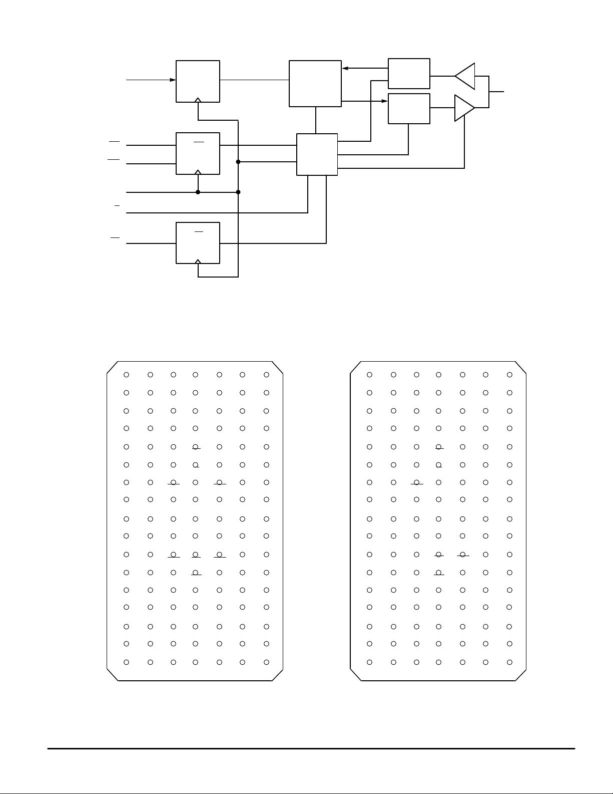
FUNCTIONAL BLOCK DIAGRAM
SA
SW
SBx
CK
SS
ADDRESS
REGISTERS
SW
REGISTERS
G
SS
REGISTERS
MEMORY
ARRAY
CONTROL
LOGIC
DATA IN
REGISTER
DQ
DATA OUT
REGISTER
PIN ASSIGNMENTS
TOP VIEW
MCM69R736A
6543217
MCM69R818A
6543217
A
V
SA SA SA SA
DDQ
B
NC NC SA NC
C
D
E
F
G
H
J
K
L
M
N
P
R
T
U
SA SA SA SA
NC
DQc DQc V
DQc
DQc
V
DQc V
DDQ
DQcDQc
DQc
DQc VSSNC DQb
V
V
V
V
DD
DDQ
DQd DQd VSSCK V
DQd V
DDQ
DQdDQd
DQd DQd VSSSA
SA SA
NC
NC
NC SA SA NC
DDQ
NC
V
DD
ZQ DQb
SS
SS
G
SS
V
V
DD
ref
CK
SBdDQdDQd
SW
SS
SS
V
V
DD
SS
SA
TDITMS
TCK
SA
V
SS
V
SS
V
SS
SBb
V
SS
V
ref
SS
V
SS
V
SS
V
SS
V
DD
TDO
NC
DQbSSV
DQb
DQbNCSBc
V
DD
DQa
DQaSBa
DQa
DQaSAV
DQa
NC
V
V
V
V
V
DDQ
NC
NC
DQb
DQb
DDQ
DQb
DQb
DDQ
DQa
DQa
DDQ
DQa
DQa
NC
ZZ
DDQ
A
B
C
D
E
F
G
H
J
K
L
M
N
P
R
T
U
SA SA SA SA
V
DDQ
NC NC SA NC
SA SA SA SA
NC
DQb NC VSSZQ DQa
DQbNC
V
NC V
DDQ
DQbNC
DQb
NC VSSNC DQa
V
V
V
V
DD
DDQ
NC DQb VSSCK V
NCDQb
DQb V
DDQ
NCDQb
NC DQb VSSSA
SA SA
NC
SA SA SA SA
NC
DDQ
NC
NC
SA
V
DD
V
SS
V
NCSSV
G
V
DD
CK
SW
V
DD
NC
TCK
SS
V
SS
V
SS
V
SS
V
ref
SS
V
SS
V
SS
V
SS
V
DD
TDO
DQa
NCNCSBb
V
NC
DQaSBa
NC
DQaSAV
NC
NC
SS
SS
V
ref
V
SS
SS
SS
V
SS
TDITMS
DD
V
V
V
V
V
DDQ
NC
NC
NC
DQa
DDQ
DQa
NC
DDQ
DQa
NC
DDQ
NC
DQa
NC
ZZ
DDQ
MCM69R736A•MCM69R818A
2
MOTOROLA FAST SRAM
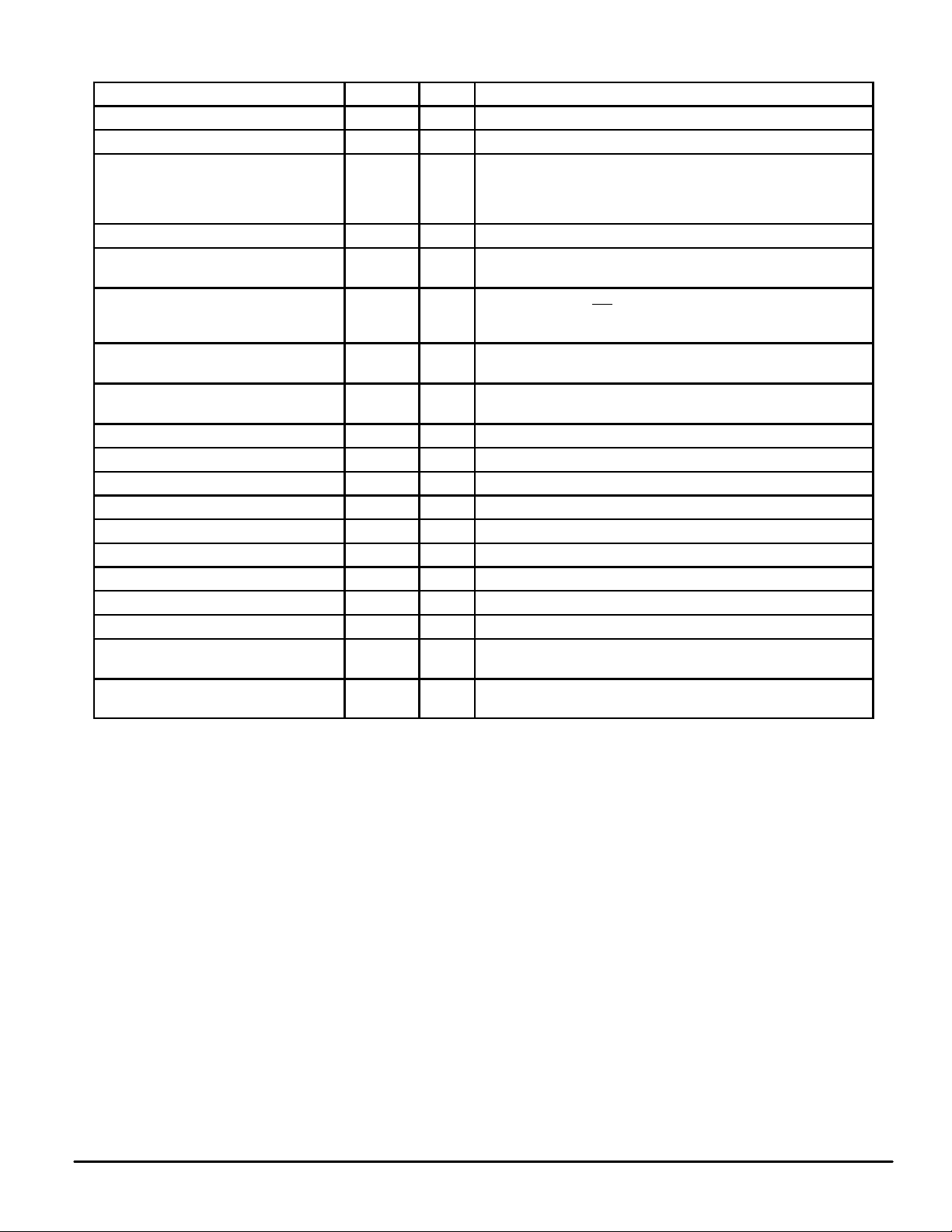
MCM69R736A PIN DESCRIPTIONS
PBGA Pin Locations Symbol
4K CK Input Address, data in and control input register clock. Active high.
4L CK Input Address, data in and control input register clock. Active low.
(a) 6K, 7K, 6L, 7L, 6M, 6N, 7N, 6P, 7P
(b) 6D, 7D, 6E, 7E, 6F, 6G, 7G, 6H, 7H
(c) 1D, 2D, 1E, 2E, 2F, 1G, 2G, 1H, 2H
(d) 1K, 2K, 1L, 2L, 2M, 1N, 2N, 1P, 2P
4F G Input Output Enable: Asynchronous pin, active low.
2A, 3A, 5A, 6A, 3B, 5B, 2C, 3C,
5C, 6C, 4N, 4P, 2R, 6R, 3T, 4T, 5T
5L, 5G, 3G, 3L
(a), (b), (c), (d)
4E SS Input Synchronous Chip Enable: Registered on the rising clock edge, active
4M SW Input Synchronous Write: Registered on the rising clock edge, active low.
4U TCK Input Test Clock (JTAG).
3U TDI Input Test Data In (JT AG).
5U TDO Output Test Data Out (JTAG).
2U TMS Input T est Mode Select (JTAG).
4D ZQ Input Programmable Output Impedance: Programming pin.
7T ZZ Input Enables sleep mode, active high.
4C, 2J, 4J, 6J, 4R, 5R V
1A, 7A, 1F, 7F, 1J, 7J, 1M, 7M, 1U, 7U V
3J, 5J V
3D, 5D, 3E, 5E, 3F, 5F, 3H, 5H,
3K, 5K, 3M, 5M, 3N, 5N, 3P, 5P, 3R
4A, 1B, 2B, 4B, 6B, 7B, 1C, 7C,
4G, 4H, 1R, 7R, 1T, 2T, 6T, 6U
Type Description
DQx I/O Synchronous Data I/O.
SA Input Synchronous Address Inputs: Registered on the rising clock edge.
SBx Input Synchronous Byte Write Enable: Enables writes to byte x in
DD
DDQ
ref
V
SS
NC — No Connection: There is no connection to the chip.
Supply Core Power Supply.
Supply Output Power Supply: provides operating power for output buffers.
Supply Input Reference: provides reference voltage for input buffers.
Supply Ground.
conjunction with the SW
low.
low.
Writes all enabled bytes.
input. Has no effect on read cycles, active
MOTOROLA FAST SRAM
MCM69R736A•MCM69R818A
3
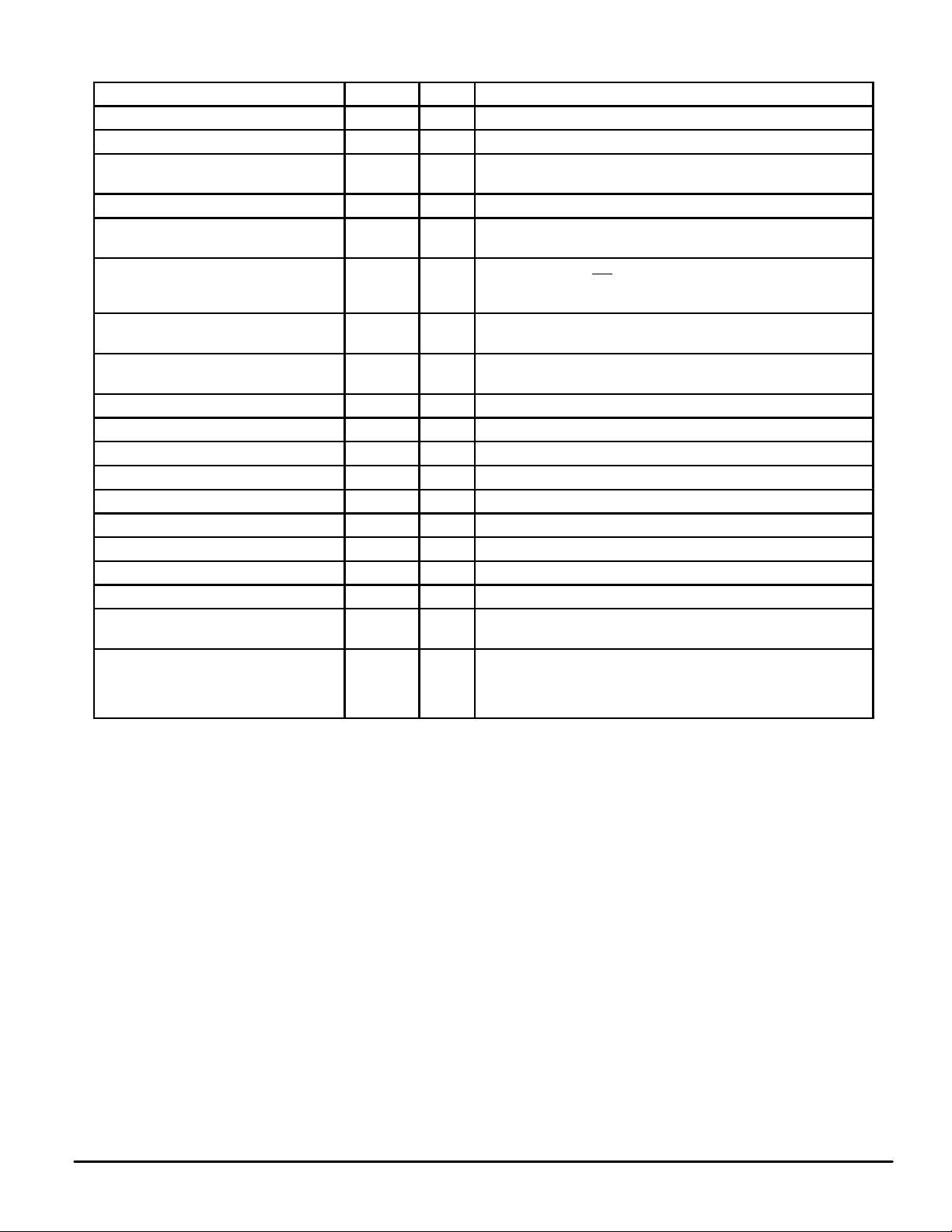
MCM69R818A PIN DESCRIPTIONS
PBGA Pin Locations Symbol
4K CK Input Address, data in and control input register clock. Active high.
4L CK Input Address, data in and control input register clock. Active low.
(a) 6D, 7E, 6F, 7G, 6H, 7K, 6L, 6N, 7P
(b) 1D, 2E, 2G, 1H, 2K, 1L, 2M, 1N, 2P
4F G Input Output Enable: Asynchronous pin, active low.
2A, 3A, 5A, 6A, 3B, 5B, 2C, 3C, 5C,
6C, 4N, 4P, 2R, 6R, 2T, 3T, 5T, 6T
5L, 3G
(a), (b)
4E SS Input Synchronous Chip Enable: Registered on the rising clock edge, active
4M SW Input Synchronous Write: Registered on the rising clock edge, active low.
4U TCK Input Test Clock (JTAG).
3U TDI Input Test Data In (JT AG).
5U TDO Output Test Data Out (JTAG).
2U TMS Input T est Mode Select (JTAG).
4D ZQ Input Programmable Output Impedance: Programming pin.
7T ZZ Input Enables sleep mode, active high.
4C, 2J, 4J, 6J, 4R, 5R V
1A, 7A, 1F, 7F, 1J, 7J, 1M, 7M, 1U, 7U V
3J, 5J V
3D, 5D, 3E, 5E, 3F, 5F, 5G, 3H, 5H,
3K, 5K, 3L, 3M, 5M, 3N, 5N, 3P, 5P, 3R
4A, 1B, 2B, 4B, 6B, 7B, 1C, 7C,
2D, 7D, 1E, 6E, 2F, 1G, 4G, 6G,
2H, 4H, 7H, 1K, 6K, 2L, 7L, 6M, 2N,
7N, 1P, 6P, 1R, 7R, 1T, 4T, 6U
Type Description
DQx I/O Synchronous Data I/O.
SA Input Synchronous Address Inputs: Registered on the rising clock edge.
SBx Input Synchronous Byte Write Enable: Enables writes to byte x in
DD
DDQ
ref
V
SS
NC — No Connection: There is no connection to the chip.
Supply Core Power Supply.
Supply Output Power Supply: provides operating power for output buffers.
Supply Input Reference: provides reference voltage for input buffers.
Supply Ground.
conjunction with the SW
low.
low.
Writes all enabled bytes.
input. Has no effect on read cycles, active
MCM69R736A•MCM69R818A
4
MOTOROLA FAST SRAM
ABSOLUTE MAXIMUM RATINGS (Voltages Referenced to V
Rating
Core Supply Voltage V
Output Supply Voltage V
Voltage On Any Pin V
Input Current (per I/O) I
Output Current (per I/O) I
Power Dissipation (See Note 2) P
Operating Temperature T
Temperature Under Bias T
Storage Temperature T
NOTES:
1. Permanent device damage may occur if ABSOLUTE MAXIMUM RATINGS are
exceeded. Functional operation should be restricted to RECOMMENDED OPERATING CONDITIONS. Exposure to higher than recommended voltages for extended
periods of time could affect device reliability.
2. Power dissipation capability will be dependent upon package characteristics and use
environment. See enclosed thermal impedance data.
Symbol Value Unit
DD
DDQ
bias
– 0.5 to VDD +
– 0.5 to VDD + 0.5 V
in
in
out
D
A
stg
, See Note 1)
SS
– 0.5 to + 4.6 V
0.5
± 50 mA
± 70 mA
— W
0 to + 70 °C
–10 to + 85 °C
– 55 to + 125 °C
This device contains circuitry to protect the
inputs against damage due to high static voltages or electric fields; however, it is advised
V
that normal precautions be taken to avoid
application of any voltage higher than maximum rated voltages to this high–impedance
circuit.
This BiCMOS memory circuit has been
designed to meet the dc and ac specifications
shown in the tables, after thermal equilibrium
has been established.
This device contains circuitry that will ensure
the output devices are in High–Z at power up.
PBGA PACKAGE THERMAL CHARACTERISTICS
Rating Symbol Max Unit Notes
Junction to Ambient (Still Air) R
Junction to Ambient (@200 ft/min) Single Layer Board R
Junction to Ambient (@200 ft/min) Four Layer Board R
Junction to Board (Bottom) R
Junction to Case (Top) R
NOTES:
1. Junction temperature is a function of on–chip power dissipation, package thermal resistance, mounting site (board) temperature, ambient
temperature, air flow, power dissipation of other components on the board, and board thermal resistance.
2. Per SEMI G38–87.
3. Indicates the average thermal resistance between the die and the printed circuit board.
4. Indicates the average thermal resistance between the die and the case top surfac e as measured by the cold plate method (MIL SPEC–883
Method 1012.1).
θJA
θJA
θJA
θJB
θJC
53 °C/W 1, 2
38 °C/W 1, 2
22 °C/W
14 °C/W 3
5 °C/W 4
CLOCK TRUTH TABLE
K ZZ SS SW SBa SBb SBc SBd DQ (n) DQ (n+1) Mode
L – H L L H X X X X X D
L – H L L L L H H H High–Z Din 0–8 Write Cycle 1st Byte
L – H L L L H L H H High–Z Din 9–17 Write Cycle 2nd Byte
L – H L L L H H L H High–Z Din 18–26 Write Cycle 3rd Byte
L – H L L L H H H L High–Z Din 27–35 Write Cycle 4th Byte
L – H L L L L L L L High–Z Din 0–35 Write Cycle All Bytes
L – H L L L H H H H High–Z High–Z Abort Write Cycle
L – H L H H X X X X X High–Z Deselect Cycle
L – H L H L X X X X High–Z High–Z Deselect Cycle
X H X X X X X X High–Z High–Z Sleep Mode
MOTOROLA FAST SRAM
0–35 Read Cycle All Bytes
out
MCM69R736A•MCM69R818A
5
DC OPERA TING CONDITIONS AND CHARACTERISTICS
(0°C ≤ TA ≤ 70°C, Unless Otherwise Noted)
RECOMMENDED OPERATING CONDITIONS
Parameter
Input Reference DC Voltage V
Core Power Supply Voltage V
Output Driver Supply Voltage V
Active Power Supply Current (x18)
Quiescent Active Power Supply Current I
Active Standby Power Supply Current I
Quiescent Standby Power Supply Current I
Sleep Mode Power Supply Current I
NOTES:
1. All data sheet parameters specified to full range of VDD unless otherwise noted. All voltages are referenced to voltage applied to VSS bumps.
2. Supply voltage applied to VDD connections.
3. Supply voltage applied to V
4. All power supply currents measured with outputs open or deselected.
5. VDD = VDD (max), t
6. VDD = VDD (max), t
7. VDD = VDD (max), t
8. VDD = VDD (max), t
9. VDD = VDD (Max), t
10. 200 mV ≥ Vin ≥ V
11. Although considerable latitude in the selection of the nominal dc value (i.e., rms value) of V
superimposed on V
DDQ
DDQ
= t
KHKH
= dc, SS
KHKH
= t
KHKH
= dc, SS
KHKH
= dc, SS
KHKH
– 200 mV.
may not exceed 5% of the dc component of V
ref
(x36)
connections.
(min), SS
KHKH
registered active.
(min), SS
KHKH
registered inactive, ZZ low.
registered inactive, ZZ high.
(See Notes 1 through 4)
Typical–5Typical–6Typical–7Typical
Symbol Min
(dc) 0.6 — — — — 1.1 V 11
ref
DD
DDQ
I
DD1
DD2
SB1
SB2
SB3
registered active, 50% read cycles.
registered inactive.
3.15 — — — — 3.6 V
1.4 — — — — 1.6 V
—
—
— 190 190 190 190 250 mA 6, 10
— 160 160 160 160 250 mA 7
— 140 140 140 140 230 mA 8, 10
— TBD TBD TBD TBD TBD mA 9, 10
ref
350
460
.
330
430
300
390
is supported, the peak to peak ac component
ref
–8
290
370
Max Unit Notes
450
560
mA 5
DC INPUT CHARACTERISTICS
Parameter Symbol Min Max Unit Notes
DC Input Logic High VIH (dc) V
DC Input Logic Low VIL (dc) – 0.3 V
Input Leakage Current I
Clock Input Signal Voltage Vin (dc) – 0.3 VDD + 0.3 V
Clock Input Differential V oltage V
Clock Input Common Mode Voltage Range (See Figure 2) VCM (dc) 0.68 1.1 V 4
Clock Input Crossing Point Voltage Range (See Figure 2) V
NOTES:
1. Inputs may undershoot to –0.5 V (peak) for up to 20% t
2. 0 V ≤ Vin ≤ V
3. Minimum instantaneous differential input voltage required for differential input clock operation.
4. Maximum rejectable common mode input voltage variation.
DDQ
for all pins.
(e.g., 2 ns at a clock cycle time of 10 ns). See Figure 2.
KHKH
lkg(1)
(dc) 0.2 VDD + 0.6 V 3
DIF
X
+ 0.1 VDD + 0.3 V
ref
– 0.1 V 1
ref
— ± 5 µA 2
0.68 1.1 V
MCM69R736A•MCM69R818A
6
MOTOROLA FAST SRAM

PROGRAMMABLE IMPEDANCE OUTPUT BUFFER OPERATION
Refer to Functional Operation section for more detailed explanation.
DC OUTPUT BUFFER CHARACTERISTICS – PROGRAMMABLE IMPEDANCE PUSH–PULL OUTPUT BUFFER MODE
(0°C ≤ TA ≤ 70°C, ZQ = IZQ (out) (RQ)) (See Notes 5 and 6)
Parameter
Output Logic Low V
Output Logic High V
Light Load Output Logic Low VOL1 V
Light Load Output Logic High VOH1 V
NOTES:
1. IOL = (V
2. | IOH | = (V
3. IOL ≤ 100 µA.
4. | IOH | ≤ 100 µA.
5. The impedance controlled mode is expected to be used in point–to–point applications, driving high impedance inputs.
6. The ZQ pin is connected through RQ to VSS for the controlled impedance mode.
/2)/(RQ/5) for values of RQ = 175 Ω ≤ RQ ≤ 350 Ω.
DDQ
/2)/(RQ/5) for values of RQ = 175 Ω ≤ RQ ≤ 350 Ω.
DDQ
Symbol Min Max Unit Notes
V
OL
OH
V
DDQ
DDQ
DDQ
/2 – 0.025 V
/2 – 0.025 V
SS
– 0.2 V
/2 + 0.025 V 1
DDQ
/2 + 0.025 V 2
DDQ
0.2 V 3
DDQ
V 4
DC OUTPUT BUFFER CHARACTERISTICS – MINIMUM IMPEDANCE PUSH–PULL OUTPUT BUFFER MODE
(0°C ≤ TA ≤ 70°C, ZQ = VDD) (See Notes 5 and 6)
Parameter
Output Logic Low VOL2 V
Output Logic High VOH2 V
Light Load Output Logic Low VOL3 V
Light Load Output Logic High VOH3 V
NOTES:
1. IOL ≤ 8 mA
2. | IOH |≤ 8 mA
3. IOL ≤ 100 µA
4. | IOH |≤ 100 µA
5. The push–pull output mode is expected to be used in bussed applications and may be series or parallel terminated. Conforms to the JEDEC
Standard JESD8–6 Class 1.
6. The ZQ pin is connected to VDD to enable the minimum impedance mode.
Symbol Min Max Unit Notes
SS
– 0.4 V
DDQ
SS
– 0.2 V
DDQ
0.4 V 1
DDQ
0.2 V 3
DDQ
V 2
V 4
CAPACITANCE (f = 1.0 MHz, dV = 3.0 V, 0°C ≤ T
Characteristic
Input Capacitance C
Input/Output Capacitance C
CK, CK Capacitance C
≤ 70°C, Periodically Sampled Rather Than 100% Tested)
A
Symbol Typ Max Unit
in
I/O
CK
4 5 pF
7 8 pF
4 5 pF
MOTOROLA FAST SRAM
MCM69R736A•MCM69R818A
7

AC OPERA TING CONDITIONS AND CHARACTERISTICS
(0°C ≤ TA ≤ 70°C, Unless Otherwise Noted)
Input Pulse Levels 0.25 to 1.25 V. . . . . . . . . . . . . . . . . . . . . . . . . . . . . .
Input Rise/Fall Time 1 V/ns (20% to 80%). . . . . . . . . . . . . . . . . . . . . .
Input Timing Measurement Reference Level 0.75 V. . . . . . . . . . . . . .
Output Timing Reference Level 0.75 V. . . . . . . . . . . . . . . . . . . . . . . . .
READ/WRITE CYCLE TIMING (See Note 1)
MCM69R736A–5
MCM69R818A–5
Parameter Symbol Min Max Min Max Min Max Min Max Unit Notes
Cycle Time t
Clock High Pulse Width t
Clock Low Pulse Width t
Clock High to Output Low–Z t
Clock High to Output Valid t
Clock High to Output Hold t
Clock High to Output High–Z t
Output Enable Low to Output
Low–Z
Output Enable Low to Output
Valid
Output Enable to Output Hold t
Output Enable High to Output
High–Z
Setup Times: Address
Hold Times: Address
NOTES:
1. In no case may control input signals (e.g., SS
(e.g., t
2. This parameter is sampled, and not 100% tested.
3. Measured at ± 200 mV from steady state.
KHKL
Data In
Chip Select
Write Enable
Data In
Chip Select
Write Enable
) or at frequencies that exceed the applied K clock frequency.
KHKH
KHKL
KLKH
KHQX1
KHQV
KHQX
KHQZ
t
GLQX
t
GLQV
GHQX
t
GHQZ
t
AVKH
t
DVKH
t
SVKH
t
WVKH
t
KHAX
t
KHDX
t
KHSX
t
KHWX
5 — 6 — 7 — 8 — ns
2 — 2.4 — 2.8 — 3.2 — ns
2 — 2.4 — 2.8 — 3.2 — ns
1 — 1 — 1 — 1 — ns
— 2.5 — 3 — 3.5 — 4 ns
0.5 — 0.5 — 0.5 — 0.5 — ns 2
— 2.5 — 3 — 3.5 — 4 ns 2, 3
0.5 — 0.5 — 0.5 — 0.5 — ns 2, 3
— 2.5 — 3 — 3.5 — 4 ns
0.5 — 0.5 — 0.5 — 0.5 — ns
— 2.5 — 3 — 3.5 — 4 ns 2, 3
0.5 — 0.5 — 0.5 — 0.5 — ns
1 — 1 — 1 — 1 — ns
) be operated with pulse widths less than the minimum clock input pulse width specifications
Clock Input Timing Reference Level Differential Cross–Point. . . . . .
ZQ for 50 Ω Impedance 250 Ω. . . . . . . . . . . . . . . . . . . . . . . . . . . . . . . .
R
Under Test TBD. . . . . . . . . . . . . . . . . . . . . . . . . . . . . . . . . . . . . . .
θJA
MCM69R736A–6
MCM69R818A–6
MCM69R736A–7
MCM69R818A–7
MCM69R736A–8
MCM69R818A–8
0.75 V
V
ref
DEVICE
UNDER
TEST
ZQ
50
250
Ω
Ω
MCM69R736A•MCM69R818A
8
V
DDQ
50
TIMING LIMITS
/2
Ω
Figure 1. T est Load
The table of timing values shows either a minimum or
a maximum limit for each parameter. Input requirements
are specified from the external system point of view.
Thus, address setup time is shown as a minimum since
the system must supply at least that much time. On the
other hand, responses from the memory are specified
from the device point of view. Thus, the access time is
shown as a maximum since the device never provides
data later than that time.
MOTOROLA FAST SRAM

AC INPUT CHARACTERISTICS
Parameter Symbol Min Max Note
AC Input Logic High (See Figure 4)
AC Input Logic Low (See Figures 2 and 4)
Input Reference Peak to Peak ac Voltage
Clock Input Differential V oltage
NOTES:
1. Inputs may undershoot to –0.5 V (peak) for up to 20% t
2. Although considerable latitude in the selection of the nominal dc value (i.e., rms value) of V
superimposed on V
3. Minimum instantaneous differential input voltage required for differential input clock operation.
may not exceed 5% of the dc component of V
ref
V
OH
V
SS
50%
100%
VIH (ac) V
VIL (ac) — V
V
(ac) — 5% V
ref
V
(ac) 400 mV V
dif
(e.g., 2 ns at a clock cycle time of 10 ns). See Figure 2.
KHKH
.
ref
+ 200 mV —
ref
20% t
KHKH
– 200 mV 1
ref
(dc) 2
ref
+ 600 mV 3
DDQ
is supported, the peak to peak ac component
ref
Figure 2. Undershoot Voltage
V
DDQ
V
TR
CROSSING POINT
V
DIF
V
CP
V
SS
*VCM, the Common Mode Input Voltage, equals VTR – ((VTR – VCP)/2).
Figure 3. Differential Inputs/Common Mode Input V oltage
V
DDQ
VIH(ac)
VCM*
V
VIL(ac)
V
MOTOROLA FAST SRAM
ref
SS
Figure 4. AC Input Conditions
MCM69R736A•MCM69R818A
9

REGISTER/REGISTER READ–WRITE–READ CYCLES
CK
SA
SS
SW
SBx
V
t
KHQZ
t
KHQX
t
KHKL
t
KLKH
A2 A3 A4
t
KHWX
t
KHQX1
t
KHQX
t
DVKH
t
KHDX
t
KHKH
t
AVKH
A0 A1
G
IL
t
SVKH
t
t
KHQV
KHAX
t
KHSX
t
WVKH
DQx
Q–1
Q0 Q1
D2 Q3
MCM69R736A•MCM69R818A
10
MOTOROLA FAST SRAM

REGISTER/REGISTER READ–WRITE–READ
Controlled)
(G
CK
SA
SS
V
SW
SBx
DQx
t
KHKH
t
AVKH
A0 A1
IL
G
t
KHAX
Q–1
t
GHQZ
Q0 Q1 D2 Q3
t
KHKL
t
KLKH
A2 A3 A4
t
GLQV
t
GLQX
t
GHQX
MOTOROLA FAST SRAM
MCM69R736A•MCM69R818A
11

FUNCTIONAL OPERATION
READ AND WRITE OPERATIONS
All control signals except G
edge of the CK clock. These signals must meet the setup
and hold times shown in the AC Characteristics table. On the
rising edge of the following clock, read data is clocked into
the output register and available at the outputs at t
ing this same cycle a new read address can be applied to the
address pins.
A deselect cycle (dead cycle) must occur prior to a write
cycle. Read cycles may follow write cycles immediately.
, SS, and SW control output drive. Chip deselect via a
G
high on SS at the rising edge of the CK clock has its effect on
the output drivers after the next rising edge of the CK clock.
low deselects the output drivers immediately (on the
SW
same cycle). Output drive is also controlled directly by output
enable, G
disable with G. G asynchronously enables the output drivers.
Output data will be valid the latter of t
Outputs will begin driving at t
vious data until t
WRITE AND BYTE WRITE FUNCTIONS
Note that in the following discussion the term “byte” refers
to nine bits of the RAM I/O bus. In all cases, the timing parameters described for synchronous write input (SW
to each of the byte write enable inputs (SBa, SBb, etc.).
Byte write enable inputs have no effect on read cycles.
This allows the system designer not interested in performing
byte writes to connect the byte enable inputs to active low
(VSS). Reads of all bytes proceed normally and write cycles,
activated via a low on SW
clock, write the entire RAM I/O width. This way the designer
is spared having to drive multiple write input buffer loads.
Byte writes are performed using the byte write enable inputs in conjunction with the synchronous write input (SW
is important to note that writing any one byte will inhibit a read
of all bytes at the current address. The RAM cannot simultaneously read one byte and write another at the same address. A write cycle initiated with none of the byte write
enable inputs active is neither a read or a write. No write will
occur, but the outputs will be deselected as in a normal write
cycle.
. No clock edges are required to generate output
or t
KHQX
are registered on the rising
. Dur-
KHQV
and t
GLQV
KHQX1
GHQX
, and the rising edge of the CK
. Outputs will hold pre-
.
KHQV
) apply
). It
LATE WRITE
The write address is sampled on the first rising edge of
clock and write data is sampled on the following rising edge.
The late write feature is implemented with single stage
write buffering. Write buffering is transparent to the user. A
comparator monitors the address bus and, when necessary,
routes buffer contents to the outputs to assure coherent operation. This occurs in all cases whether there is a byte write
or a full word is written.
PROGRAMMABLE IMPEDANCE OPERATION
The designer can program the RAMs output buffer impedance by terminating the ZQ
resistor (RQ). The value of RQ is five times the output impedance desired. For example, 250 Ω resistor will give an output
impedance of 50 Ω.
Impedance updates occur continuously and the frequency
of the update is based on the subdivided K clock. Note that if
the K clock stops so does the impedance update.
.
The actual change in the impedance occurs in small increments and is monotonic. There are no significant disturbances that occur on the output because of this smooth
update method.
The impedance update is not related to any particular type
of cycle because the impedance is updated continuously and
is based on the K clock. Updates occur regardless of whether the the device is performing a read, write or a deselect
cycle and does not depend on the state of G
At power up, the output impedance defaults to approximately 50 ohms. It will take 4,000 to 16,000 cycles for the impedance to be completely updated if the programmed
impedance is much higher or lower than 50 Ω.
The output buffers can also be programmed in a minimum
impedance configuration by connecting ZQ to VDD.
POWER UP AND INITIALIZATION
The following supply voltage application sequence is recommended: VSS, VDD, then V
solute Maximum Ratings table, V
0.5 V, whatever the instantaneous value of VDD. Once supplies have reached specification levels, a minimum dwell of
1.0 ms with C/K clock inputs cycling is required before beginning normal operations. At power up the output impedance
will be set at approximately 50 Ω as stated above.
pin to VSS through a precision
.
. Please note, per the Ab-
DDQ
is not to exceed VDD +
DDQ
MCM69R736A•MCM69R818A
12
MOTOROLA FAST SRAM

SERIAL BOUNDARY SCAN TEST ACCESS PORT OPERATION
OVERVIEW
1 149.1 compliant T APs. The TAP operates using conventional JEDEC Standard 8–1B Low Voltage (3.3 V) TTL / CMOS
The serial boundary scan test access port (TAP) on this
RAM is designed to operate in a manner consistent with
IEEE Standard 1149.1–1990 (commonly referred to as
JTAG), but does not implement all of the functions required
for 1149.1 compliance. Certain functions have been modified
or eliminated because their implementation places extra delays in the RAMs critical speed path. Nevertheless, the RAM
supports the standard TAP controller architecture. (The TAP
controller is the state machine that controls the TAPs operation) and can be expected to function in a manner that does
not conflict with the operation of devices with Standard
logic level signaling.
DISABLING THE TEST ACCESS PORT
It is possible to use this device without utilizing the TAP. To
disable the T AP Controller without interfering with normal operation of the device, TCK must be tied to VSS to preclude
mid level inputs. TDI and TMS are designed so an undriven
input will produce a response identical to the application of a
logic 1, and may be left unconnected. But they may also be
tied to VDD through a 1 k resistor. TDO should be left unconnected.
T AP DC OPERATING CHARACTERISTICS
(0°C ≤ TA ≤ 70°C, Unless Otherwise Noted)
Parameter
Logic Input Logic High VIH1 2.0 VDD + 0.3 V
Logic Input Logic Low VIL1 – 0.3 0.8 V
Logic Input Leakage Current I
CMOS Output Logic Low VOL1 — 0.2 V 2
CMOS Output Logic High VOH1 VDD – 0.2 — V 3
TTL Output Logic Low VOL2 — 0.4 V 4
TTL Output Logic High VOH2 2.4 — V 5
NOTES:
1. 0 V ≤ Vin ≤ V
2. IOL1 ≤ 100 µA @ VOL = 0.2 V. Sampled, not 100% tested.
3. |IOH1| ≤ 100 µA @ V
4. IOL2 ≤ 8 mA @ VOL = 0.4 V.
5. |IOH2| ≤ 8 mA @ VOH = 2.4 V.
for all logic input pins.
DDQ
– 0.2 V. Sampled, not 100% tested.
DDQ
Symbol Min Max Unit Note
lkg
— ± 5 µA 1
MOTOROLA FAST SRAM
MCM69R736A•MCM69R818A
13

T AP AC OPERATING CONDITIONS AND CHARACTERISTICS
(0°C ≤ TA ≤ 70°C, Unless Otherwise Noted)
Input Pulse Levels 0 to 3.0 V. . . . . . . . . . . . . . . . . . . . . . . . . . . . . . . . .
Input Rise/Fall Time 1 V/ns (20% to 80%). . . . . . . . . . . . . . . . . . . . . .
Input Timing Measurement Reference Level 1.5 V. . . . . . . . . . . . . . .
Output Timing Reference Level 1.5 V. . . . . . . . . . . . . . . . . . . . . . . . . .
TAP CONTROLLER TIMING
Parameter Symbol Min Max Unit Notes
Cycle Time t
Clock High Time t
Clock Low Time t
TMS Setup t
TMS Hold t
TDI Valid to TCK High t
TCK High to TDI Don’t Care t
Capture Setup t
Capture Hold t
TCK Low to TDO Unknown t
TCK Low to TDO Valid t
NOTES:
1. tCS + tCH defines the minimum pause in RAM I/O pad transitions to assure accurate pad data capture.
Output Test Load 50 Ω Parallel Terminated T–line with 20 pF. . . . . .
Test Load Termination Supply Voltage (VT) 1.5 V. . . . . . . . . . . . . . .
THTH
THTL
TLTH
MVTH
THMX
DVTH
THDX
CS
CH
TLQX
TLOV
100 — ns
40 — ns
40 — ns
10 — ns
10 — ns
10 — ns
10 — ns
10 — ns 1
10 — ns 1
0 — ns
— 20 ns
Receiver Input Capacitance
TEST CLOCK
(TCK)
TEST MODE SELECT
(TMS)
TEST DATA IN
(TDI)
TEST DATA OUT
(TDO)
t
THTL
AC TEST LOAD
DEVICE
UNDER
TEST
TAP CONTROLLER TIMING DIAGRAM
t
THTH
t
TLTH
t
MVTH
t
DVTH
50
t
THDX
Ω
t
THMX
1.5 V
t
TLQV
t
TLQX
50
Ω
20 pF
MCM69R736A•MCM69R818A
14
MOTOROLA FAST SRAM

TEST ACCESS PORT PINS
TCK – TEST CLOCK (INPUT)
Clocks all TAP events. All inputs are captured on the rising
edge of TCK and all outputs propagate from the falling edge
of TCK.
TMS – TEST MODE SELECT (INPUT)
The TMS input is sampled on the rising edge of TCK. This
is the command input for the TAP controller state machine.
An undriven TMS input will produce the same result as a logic one input level.
TDI – TEST DATA IN (INPUT)
The TDI input is sampled on the rising edge of TCK. This is
the input side of the serial registers placed between TDI and
TDO. The register placed between TDI and TDO is determined by the state of the TAP controller state machine and
the instruction that is currently loaded in the TAP instruction
register (refer to Figure 6 T AP Controller State Diagram). An
undriven TDI pin will produce the same result as a logic one
input level.
TDO – TEST DATA OUT (OUTPUT)
Output that is active depending on the state of the TAP
state machine (refer to Figure 6 TAP Controller State Diagram). Output changes in response to the falling edge of
TCK. This is the output side of the serial registers placed between TDI and TDO.
TRST – TAP RESET
This device does not have a TRST pin. TRST is optional in
IEEE 1149.1. The test–logic reset state is entered while TMS
is held high for five rising edges of TCK. Power on reset circuitry is included internally. This type of reset does not affect
the operation of the system logic. The reset affects test logic
only .
TEST ACCESS PORT REGISTERS
OVERVIEW
The various TAP registers are selected (one at a time) via
the sequences of ones and zeros input to the TMS pin as the
TCK is strobed. Each of the TAPs registers are serial shift
registers that capture serial input data on the rising edge of
TCK and push serial data out on subsequent falling edge of
TCK. When a register is selected it is “placed” between the
TDI and TDO pins.
INSTRUCTION REGISTER
The instruction register holds the instructions that are
executed by the T AP controller when it is moved into the run
test/idle or the various data register states. The instructions
are three bits long. The register can be loaded when it is
placed between the TDI and TDO pins. The instruction register is automatically preloaded with the IDCODE instruction at
power–up or whenever the controller is placed in test–logic–
reset state.
BYPASS REGISTER
The bypass register is a single bit register that can be
placed between TDI and TDO. It allows serial test data to be
passed through the RAMs T AP to another device in the scan
chain with as little delay as possible.
BOUNDARY SCAN REGISTER
The boundary scan register is identical in length to the
number of active input and I/O connections on the RAM (not
counting the T AP pins). This also includes a number of place
holder locations (always set to a logic 1) reserved for density
upgrade address pins. There are a total of 70 bits in the case
of the x36 device and 51 bits in the case of the x18 device.
The boundary scan register, under the control of the TAP
controller, is loaded with the contents of the RAMs I/O ring
when the controller is in capture–DR state and then is placed
between the TDI and TDO pins when the controller is moved
to shift–DR state. Several TAP instructions can be used to
activate the boundary scan register.
The Bump/Bit Scan Order tables describe which device
bump connects to each boundary scan register location. The
first column defines the bit’s position in the boundary scan
register. The shift register bit nearest TDO (i.e., first to be
shifted out) is defined as bit 1. The second column is the
name of the input or I/O at the bump and the third column is
the bump number.
IDENTIFICATION (ID) REGISTER
The ID Register is a 32 bit register that is loaded with a device and vendor specific 32 bit code when the controller is
put in capture–DR state with the IDCODE command loaded
in the instruction register. The code is loaded from a 32 bit
on–chip ROM. It describes various attributes of the RAM as
indicated below. The register is then placed between the TDI
and TDO pins when the controller is moved into shift–DR
state. Bit 0 in the register is the LSB and the first to reach
TDO when shifting begins.
ID Register Presence Indicator
Bit # 0
Value 1
Motorola JEDEC ID Code (Compressed Format, per
IEEE Standard 1149.1 – 1990
Bit # 11 10 9 8 7 6 5 4 3 2 1
Value 0 0 0 0 0 0 0 1 1 1 0
Reserved For Future Use
Bit # 17 16 15 14 13 12
Value x x x x x x
Device Width
Configuration Bit # 22 21 20 19 18
128Kx36 Value 0 0 1 0 0
256Kx18 Value 0 0 0 1 1
Device Depth
Configuration Bit # 27 26 25 24 23
128Kx36 Value 0 0 1 0 1
256Kx18 Value 0 0 1 1 0
Revision Number
Bit # 31 30 29 28
Value x x x x
Figure 5. ID Register Bit Meanings
MOTOROLA FAST SRAM
MCM69R736A•MCM69R818A
15

MCM69R736A Bump/Bit Scan Order
BIT#Signal
Bump
Bit#Signal
Bump
Bit#Signal
Bump
Bit#Signal
Bump
BIT Signal Bump Bit Signal Bump
Name
1 M2 5R 36 SA 3B
2 SA 4P 37 NC 2B
3 SA 4T 38 SA 3A
4 SA 6R 39 SA 3C
5 SA 5T 40 SA 2C
6 ZZ 7T 41 SA 2A
7 DQa 6P 42 DQc 2D
8 DQa 7P 43 DQc 1D
9 DQa 6N 44 DQc 2E
10 DQa 7N 45 DQc 1E
11 DQa 6M 46 DQc 2F
12 DQa 6L 47 DQc 2G
13 DQa 7L 48 DQc 1G
14 DQa 6K 49 DQc 2H
15 DQa 7K 50 DQc 1H
16 SBa 5L 51 SBc 3G
17 CK 4L 52 ZQ 4D
18 CK 4K 53 SS 4E
19 G 4F 54 NC 4G
20 SBb 5G 55 NC 4H
21 DQb 7H 56 SW 4M
22 DQb 6H 57 SBd 3L
23 DQb 7G 58 DQd 1K
24 DQb 6G 59 DQd 2K
25 DQb 6F 60 DQd 1L
26 DQb 7E 61 DQd 2L
27 DQb 6E 62 DQd 2M
28 DQb 7D 63 DQd 1N
29 DQb 6D 64 DQd 2N
30 SA 6A 65 DQd 1P
31 SA 6C 66 DQd 2P
32 SA 5C 67 SA 3T
33 SA 5A 68 SA 2R
34 NC 6B 69 SA 4N
35 SA 5B 70 M1 3R
NOTES:
1. The NC pads listed in this table are indeed no connects, but are represented in the boundary scan register by a “place holder” bit that is forced
to logic 1. These pads are reserved for use as address inputs on higher density RAMs that follow this pad out and scan order standard.
2. In scan mode, differential inputs CK and CK
3. ZQ, M1 and M2 are not ordinary inputs and may not respond to standard I/O logic levels. ZQ, M1 and M2 must be driven to within 100 mV
of a VDD or VSS supply rail to ensure consistent results.
4. ZZ must remain at VIL during boundary scan to ensure consistent results.
ID
Name
are referenced to each other and must be at opposite logic levels for reliable operation.
ID
MCM69R818A Bump/Bit Scan Order
Bit Signal Bump Bit Signal Bump
Name
1 M2 5R 36 SBb 3G
2 SA 6T 37 ZQ 4D
3 SA 4P 38 SS 4E
4 SA 6R 39 NC 4G
5 SA 5T 40 NC 4H
6 ZZ 7T 41 SW 4M
7 DQa 7P 42 DQb 2K
8 DQa 6N 43 DQb 1L
9 DQa 6L 44 DQb 2M
10 DQa 7K 45 DQb 1N
11 SBa 5L 46 DQb 2P
12 CK 4L 47 SA 3T
13 CK 4K 48 SA 2R
14 G 4F 49 SA 4N
15 DQa 6H 50 SA 2T
16 DQa 7G 51 M1 3R
17 DQa 6F
18 DQa 7E
19 DQa 6D
20 SA 6A
21 SA 6C
22 SA 5C
23 SA 5A
24 NC 6B
25 SA 5B
26 SA 3B
27 NC 2B
28 SA 3A
29 SA 3C
30 SA 2C
31 SA 2A
32 DQb 1D
33 DQb 2E
34 DQb 2G
35 DQb 1H
ID
Name
ID
MCM69R736A•MCM69R818A
16
MOTOROLA FAST SRAM

T AP CONTROLLER INSTRUCTION SET
OVERVIEW
There are two classes of instructions defined in the Standard 1149.1–1990; the standard (public) instructions, and device specific (private) instructions. Some public instructions,
are mandatory for 1149.1 compliance. Optional public
instructions must be implemented in prescribed ways.
Although the TAP controller in this device follows the
1 149.1 conventions, it is not 1194.1 compliant because some
of the mandatory instructions are not fully implemented. The
TAP on this device may be used to monitor all input and I/O
pads, but cannot be used to load address, data or control signals into the RAM or to preload the I/O buffers. In other
words, the device will not perform Standard 1 149.1 EXTEST,
INTEST or the preload portion of the SAMPLE / PRELOAD
command.
When the TAP controller is placed in capture–IR state the
two least significant bits of the instruction register are loaded
with 01. When the controller is moved to the shift–IR state
the instruction register is placed between TDI and TDO. In
this state the desired instruction is serially loaded through the
TDI input (while the previous contents are shifted out at
TDO). For all instructions, the TAP executes newly loaded
instructions only when the controller is moved to update–IR
state. The T AP instruction sets for this device are listed in the
following tables.
ST ANDARD (PUBLIC) INSTRUCTIONS
BYPASS
The BYPASS instruction is loaded in the instruction register when the bypass register is placed between TDI and
TDO. This occurs when the TAP controller is moved to the
shift–DR state. This allows the board level scan path to be
shortened to facilitate testing of other devices in the scan
path.
SAMPLE/PRELOAD
Sample/preload is a Standard 1149.1 mandatory public
instruction. When the sample / preload instruction is loaded
in the Instruction register, moving the TAP controller into the
capture–DR state loads the data in the RAMs input and I/O
buffers into the boundary scan register. Because the RAM
clock(s) are independent from the TAP clock (TCK) it is possible for the TAP to attempt to capture the I/O ring contents
while the input buffers are in transition (i.e. in a metastable
state). Although allowing the TAP to sample metastable inputs will not harm the device, repeatable results cannot be
expected. RAM input signals must be stabilized for long
enough to meet the T APs input data capture set–up plus hold
time (tCS plus tCH). The RAMs clock inputs need not be
paused for any other T AP operation except capturing the I/O
ring contents into the boundary scan register.
Moving the controller to shift–DR state then places the
boundary scan register between the TDI and TDO pins. Because the PRELOAD portion of the command is not implemented in this device, moving the controller to the
update–DR state with the SAMPLE / PRELOAD instruction
loaded in the instruction register has the same effect as the
pause–DR command. This functionality is not Standard
1 149.1 compliant.
EXTEST
EXTEST is an IEEE 1149.1 mandatory public instruction. It
is to be executed whenever the instruction register, whatever
length it may be in the device, is loaded with all logic 0s.
EXTEST is not implemented in this device. Therefore this
device is not 1149.1 compliant. Nevertheless, this RAMs TAP
does respond to an all zeros instruction, as follows. With the
EXTEST (000) instruction loaded in the instruction register
the RAM responds just as it does in response to the
SAMPLE / PRELOAD instruction described above, except
the RAM outputs are forced to high–Z any time the
instruction is loaded.
IDCODE
The IDCODE instruction causes the ID ROM to be loaded
into the ID register when the controller is in capture–DR
mode and places the ID register between the TDI and TDO
pins in shift–DR mode. The IDCODE instruction is the default
instruction loaded in at power up and any time the controller
is placed in the test–logic–reset state.
THE DEVICE SPECIFIC (PUBLIC) INSTRUCTION
SAMPLE–Z
If the SAMPLE–Z instruction is loaded in the instruction
register, all RAM outputs are forced to an inactive drive state
(high–Z) and the boundary scan register is connected between TDI and TDO when the T AP controller . is moved to the
shift–DR state.
THE DEVICE SPECIFIC (PRIV ATE) INSTRUCTION
NOOP
Do not use these instructions; they are reserved for future
use.
MOTOROLA FAST SRAM
MCM69R736A•MCM69R818A
17

STANDARD (PUBLIC) INSTRUCTION CODES
Instruction Code* Description
EXTEST 000 Captures I/O ring contents. Places the boundary scan register between TDI and TDO. Forces all
IDCODE 001** Preloads ID register and places it between TDI and TDO.
SAMPLE / PRELOAD 100 Captures I/O ring contents. Places the boundary scan register between TDI and TDO. Does not
BYPASS 111 Places bypass register between TDI and TDO.
SAMPLE–Z 010 Captures I/O ring contents. Places the boundary scan register between TDI and TDO. Forces all
*Instruction codes expressed in binary, MSB on left, LSB on right.
**Default instruction automatically loaded at power–up and in test–logic–reset state.
RAM outputs to High–Z state. *NOT 1149.1 COMPLIANT*
Does not affect RAM operation.
affect RAM operation.
Does not implement 1149.1 Preload function. * NOT 1149.1 COMPLIANT *
Does not affect RAM operation.
RAM output drivers to High–Z.
STANDARD (PRIVATE) INSTRUCTION CODES
Instruction Code* Description
NO OP 011 Do not use these instructions; they are reserved for future use.
NO OP 101 Do not use these instructions; they are reserved for future use.
NO OP 110 Do not use these instructions; they are reserved for future use.
*Instruction codes expressed in binary, MSB on left, LSB on right.
TEST–LOGIC
1
RUN–TEST/
0
RESET
0
IDLE
1
1
0
SELECT
DR–SCAN
0
CAPTURE–DR
0
SHIFT–DR
1
EXIT1–DR
0
PAUSE–DR
1
EXIT2–DR
1
UPDATE–DR
1
1
0
1
0
0
SELECT
IR–SCAN
CAPTURE–IR
SHIFT–IR
EXIT1–IR
PAUSE–IR
EXIT2–IR
UPDATE–IR
1
0
0
0
1
1
0
0
1
1
NOTE: The value adjacent to each state transition represents the signal present at TMS at the rising edge of TCK.
MCM69R736A•MCM69R818A
18
11
0
Figure 6. TAP Controller State Diagram
0
MOTOROLA FAST SRAM

Motorola Memory Prefix
Part Number
ORDERING INFORMATION
(Order by Full Part Number)
69R736A
MCM 69R818A XX X X
R = Tape and Reel, Blank = Tray
Speed (5 = 5 ns, 6 = 6 ns, 7 = 7 ns, 8 = 8 ns)
Package (ZP = PBGA)
Full Part Numbers — MCM69R736AZP5 MCM69R736AZP6 MCM69R736AZP7 MCM69R736AZP8
MCM69R818AZP5 MCM69R818AZP6 MCM69R818AZP7 MCM69R818AZP8
MCM69R736AZP5R MCM69R736AZP6R MCM69R736AZP7R MCM69R736AZP8R
MCM69R818AZP5R MCM69R818AZP6R MCM69R818AZP7R MCM69R818AZP8R
MOTOROLA FAST SRAM
MCM69R736A•MCM69R818A
19

P ACKAGE DIMENSIONS
ZP PACKAGE
7 X 17 BUMP PBGA
CASE 999–01
PIN 1A
IDENTIFIER
P
A
–W–
N
TOP VIEW
F
C
E
4X
–L–
K
0.20 (0.008)
B
SIDE VIEW
S
16X
0.35 (0.014) T
G
6X G
BOTTOM VIEW
7654321
R
A
B
C
D
E
F
G
H
J
K
L
M
N
P
R
T
U
119X
D
0.10 (0.004)ST
0.25 (0.010) T
0.15 (0.006) T
–T–
NOTES:
1. DIMENSIONING AND TOLERANCING PER ANSI
Y14.5M, 1982.
2. CONTROLLING DIMENSION: MILLIMETER.
MILLIMETERS
DIMAMIN MAX MIN MAX
14.00 BSC 0.551 BSC
B 22.00 BSC 0.866 BSC
C ––– 2.40 ––– 0.094
D 0.60 0.90 0.024 0.035
E 0.50 0.70 0.020 0.028
F 1.30 1.70 0.051 0.067
G 1.27 BSC 0.050 BSC
K 0.80 1.00 0.031 0.039
N 11.90 12.10 0.469 0.476
P 19.40 19.60 0.764 0.772
R 7.62 BSC 0.300 BSC
S 20.32 BSC 0.800 BSC
SS
L0.30 (0.012)STW
INCHES
Motorola reserves the right to make changes without further notice to any products herein. Motorola makes no warranty , representation or guarantee regarding
the suitability of its products for any particular purpose, nor does Motorola assume any liability arising out of the application or use of any product or circuit, and
specifically disclaims any and all liability, including without limitation consequential or incidental damages. “T ypical” parameters which may be provided in Motorola
data sheets and/or specifications can and do vary in different applications and actual performance may vary over time. All operating parameters, including “Typicals”
must be validated for each customer application by customer’s technical experts. Motorola does not convey any license under its patent rights nor the rights of
others. Motorola products are not designed, intended, or authorized for use as components in systems intended for surgical implant into the body, or other
applications intended to support or sustain life, or for any other application in which the failure of the Motorola product could create a situation where personal injury
or death may occur. Should Buyer purchase or use Motorola products for any such unintended or unauthorized application, Buyer shall indemnify and hold Motorola
and its officers, employees, subsidiaries, affiliates, and distributors harmless against all claims, costs, damages, and expenses, and reasonable attorney fees
arising out of, directly or indirectly, any claim of personal injury or death associated with such unintended or unauthorized use, even if such claim alleges that
Motorola was negligent regarding the design or manufacture of the part. Motorola and are registered trademarks of Motorola, Inc. Motorola, Inc. is an Equal
Opportunity/Affirmative Action Employer.
Mfax is a trademark of Motorola, Inc.
How to reach us:
USA/EUROPE /Locations Not Listed: Motorola Literature Distribution; JAPAN: Nippon Motorola Ltd.: SPD, Strategic Planning Office, 4–32–1,
P.O. Box 5405, Denver, Colorado 80217. 1–303–675–2140 or 1–800–441–2447 Nishi–Gotanda, Shinagawa–ku, Tokyo 141, Japan. 81–3–5487–8488
Customer Focus Center: 1–800–521–6274
Mfax: RMFAX0@email.sps.mot.com – TOUCHTONE 1–602–244–6609 ASIA/PACIFIC: Motorola Semiconductors H.K. Ltd.; 8B Tai Ping Industrial Park,
Moto rola Fax Back Syste m – US & Canada ONLY 1–800–774–1848 51 Ting Kok Road, Tai Po, N.T., Hong Kong. 852–26629298
– http://sps.motorola.com/mfax/
HOME PAGE: http://motorola.com/sps/
MCM69R736A•MCM69R818A
◊
MOTOROLA FAST SRAM
MCM69R736A/D
20
 Loading...