

Motorola MCC141800AZ Datasheet
3–277
MC141800AMOTOROLA
Product Preview
LCD Segment / Common Driver
CMOS
MC141800A is a CMOS LCD Driver which consists of 193 high voltage
LCD driving signals to drive 128 Segment and 65 Common display. It has
6800-series parallel, IIC serial interface and Serial Peripheral interface (SPI)
capability for operating with general MCU. Besides the general LCD driver
features, it has on chip LCD Smart Bias Divider circuit such that minimize
external component required in applications.
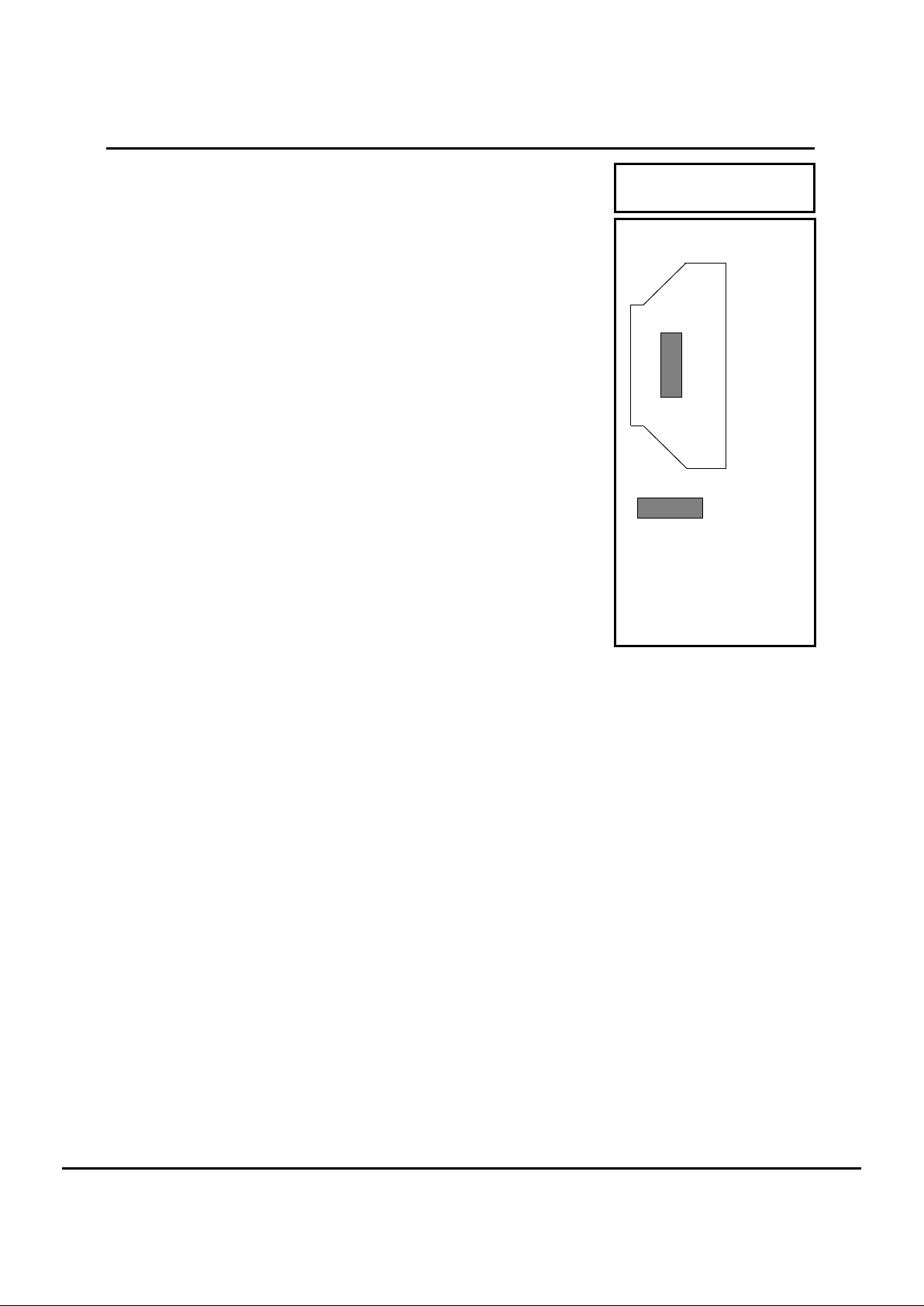
MC141800AT: TAB (Tape Automated Bonding)
MCC141800AZ: Gold Bump Die
• Single Supply Operation, 2.4 V - 3.5 V
• Maximum 16.5V LCD Driving Output Voltage
• Low Current Stand-by Mode (<1uA)
• On Chip Internal DC/DC Converter / External Power Supply
• Smart Bias Divider
• 4X / 5X DC-DC Converter
• 8 bit 6800-series Parallel Interface, 1 MHz IIC Serial Interface and
Serial Peripheral Interface (SPI)
• On chip Oscillator
• Graphic Mode Operation
• On Chip 128 x 65 Display Data RAM
• Master Clear RAM
• Low Power Icon Mode (128 icons, <25uA)
• Display Masks for Implementation of Blinking Effect
• 1 to 65 Selectable Multiplex Ratio
• 1:7 / 1:9 Bias Ratio
• Re-mapping of Row and Column Drivers
• 16 level Internal Contrast Control
• External Contrast Control
• Built-in Temperature Compensation Circuit
• Selectable Display Waveform: Type B or Type C Waveform
• 2V Icon Mode Display On
MC141800A
ORDERING INFORMATION
MC141800AT 70 mm TAB
MCC141800AZ Gold Bump Die
This document contains information on a product under development. Motorola reserves the right to change or discontinue this product without notice.
TAB
MC141800AT
MCC141800AZ
Gold bump die
MOTOROLA
SEMICONDUCTOR TECHNICAL DATA
REV O
2/97
MOTOROLA
3–278
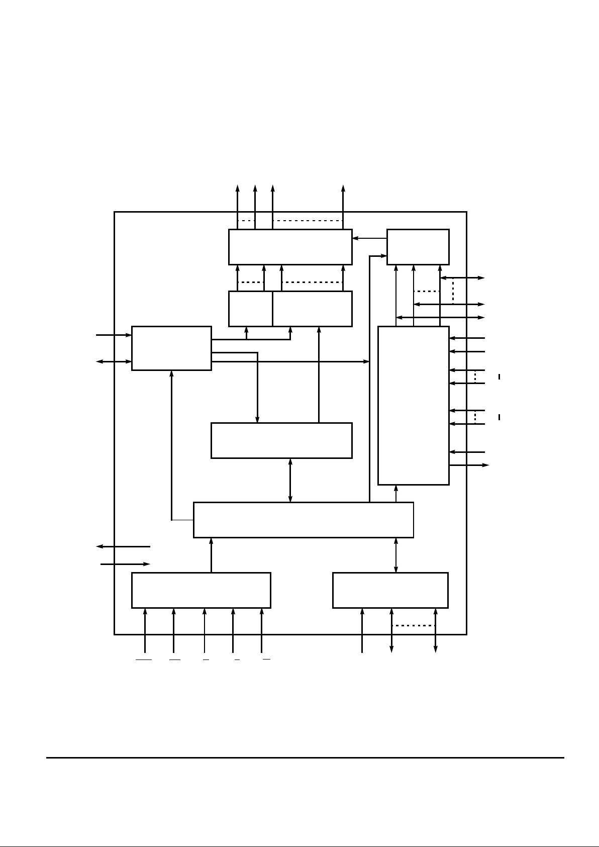
MC141800A
LCD Driving
Voltage Generator
4x and 5x
DC/DC Converter,
Voltage Regulator,
Smart Bias Divider,
Contrast Control,
Temperature
Compensation
Com0 to
Com64
Seg0~Seg127
OSC1
OSC2
DVSS
DVDD
RES
R/
W
D0~D7
VLL6
VLL2
VCC
VR
VF
C1P
C3P
C1N
C3N
AVDD
AVSS
GDDRAM
65 x 128Bits
Command Decoder
Parallel / Serial InterfaceCommand Interface
Display
Timing
Generator
128 Bit Latch
65 Bit
Latch
HV Buffer Cell Level Shifter
Level
Selector
CLK
D/
CCE S/P
Block Diagram
3–279
MC141800AMOTOROLA
MC141800AT PIN ASSIGNMENT
(COPPER VIEW)
1234567891011121314151617181920212223242526272829303132333435363738394041
42
DVDD
S/
P
RES
D/
C
R/
W
D7/IIC/
SPI
D6
D5
D4/Dout
D3/Din
D2/A2
D1/A1
D0/SDA
CLK
CEVFVR
C1P
C1N
C2P
C2N
C3P
C3N
NC
NC
VLL2
VLL3
NCNCNC
NC
VLL4
VLL5
VLL6
OSC1
DVSS
NC
NC
VCC
AVSS
OSC2
AVDD
COM31
COM30
COM29
COM28
COM27
COM2
COM1
COM0
COM64B
SEG127
SEG126
SEG125
SEG124
SEG123
SEG66
SEG65
SEG64
SEG63
SEG62
SEG61
SEG2
SEG1
SEG0
COM32
COM33
COM34
COM61
COM62
COM63
COM64A
DUMMY
DUMMY
DUMMY
DUMMY
236
235
234
233
232
207
206
205
204
203
202
201
200
199
142
141
140
139
138
137
7877767574
73
464544
43
Mirror Design TAB
DIE
ENCAPSULANT
COPPER
POLYIMIDE
MOTOROLA
3–280
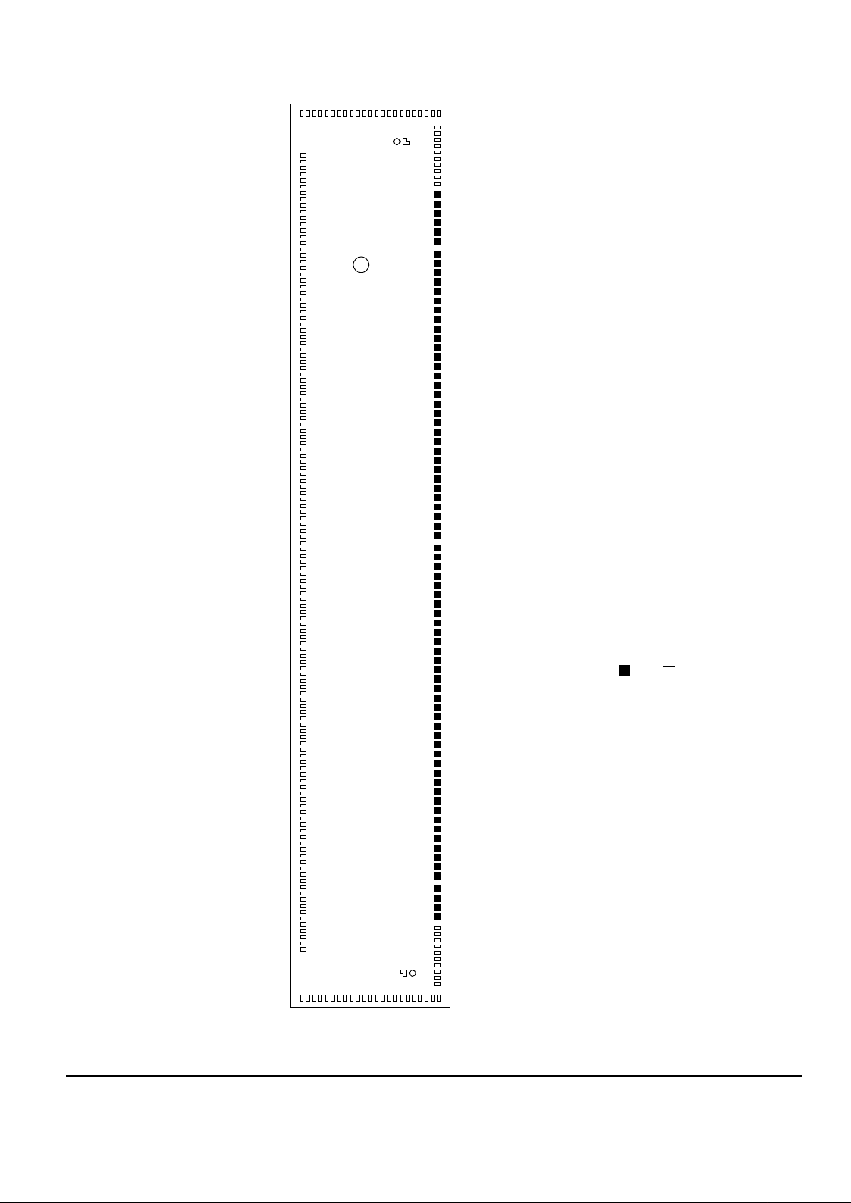
MC141800A
Input Pad, 65 x 65 (um)
Output Pad, 42 x 100 (um)
Die Pad Layout for MC141800A
COM55
COM56
.
.
COM63
COM64A
AVDD
OSC2
AVSS
VCC
VCC
DVSS
DVSS
OSC1
DVSS
VLL6
VLL6
VLL5
VLL5
VLL4
VLL4
VLL3
VLL3
VLL2
VLL2
C3N
C3P
C2N
C2P
C1N
C1P
VR
VF
AVSS
AVSS
AVDD
AVDD
COM31
.
.
.
.
.
COM22
COM32
COM33...........COM53
COM54
SEG0
SEG1
SEG2
.
.
.
.
.
.
.
.
.
.
.
.
.
.
.
.
.
.
.
.
.
.
.
.
.
.
.
.
.
.
.
.
.
.
.
.
.
.
.
.
.
.
.
.
.
.
.
.
.
.
.
.
.
.
.
.
.
.
.
.
.
.
.
.
.
.
.
.
.
.
.
.
.
.
.
.
.
SEG126
SEG127
COM64B
COM0
...........
COM20
COM21
Gold Bump Size :
MC141800A
DVSS
DVSS
DVSS
DVSS
DVSS
DVSS
D/C
RES
S/P
DVDD
DVSS
DVSS
DVDD
DVDD
CE
CLK
CLK
D0
D0
D1
D2
D3
D4
D5
D6
D7
R/W
DVSS
DVSS
DVSS
DVSS
DVSS
DVSS
DVSS
DVSS
DVSS
DVSS
DVSS
DVSS
DVSS
DVSS
DVSS
DVSS
DVSS
DVSS
DVSS
M
3–281
MC141800AMOTOROLA
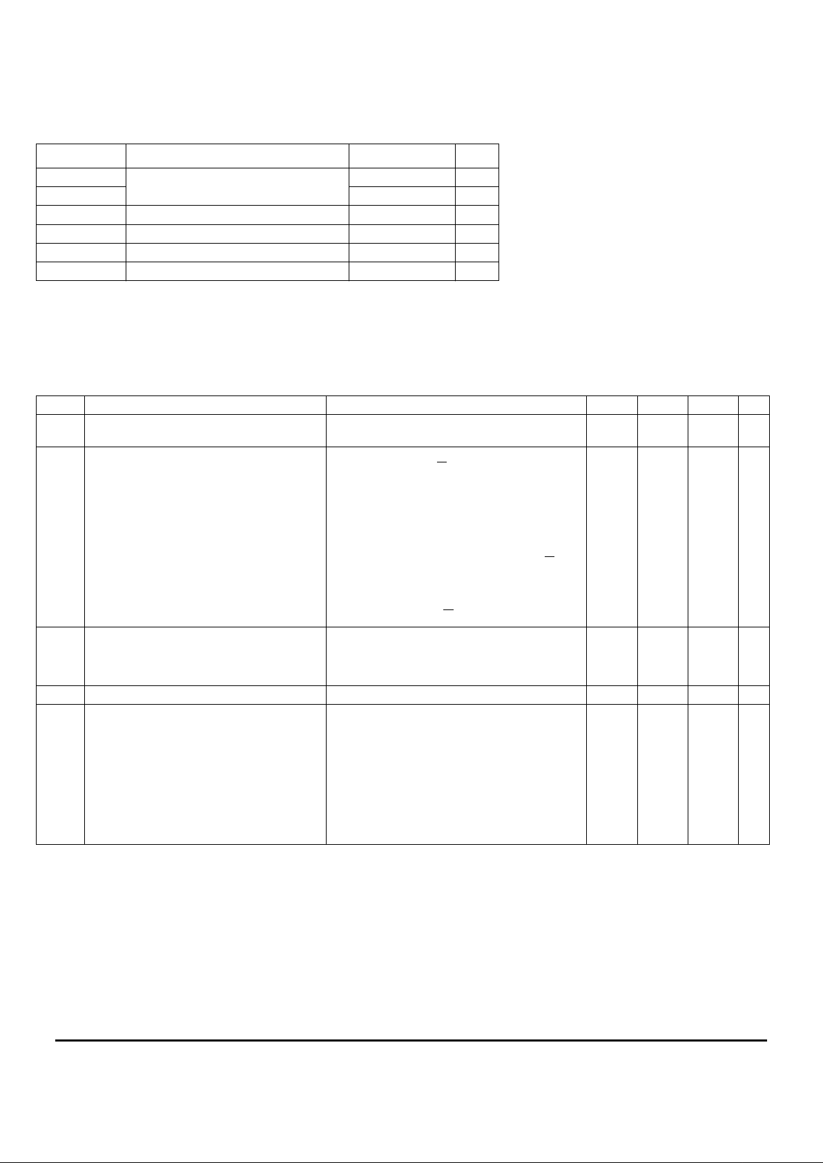
MAXIMUM RATINGS* (Voltages Referenced to V
SS
, TA=25˚C)
Symbol Parameter Value Unit
AV
DD
,DV
DD
Supply Voltage -0.3 to +4.0 V
V
CC
VSS-0.3 to VSS+16.5 V
V
in
Input Voltage VSS-0.3 to VDD+0.3 V
I Current Drain Per Pin Excluding VDD and V
SS
25 mA
T
A
Operating Temperature -30 to +85 ˚C
T
stg
Storage Temperature Range -65 to +150 ˚C
* Maximum Ratings are those values beyond which damage to the device may occur. Functional
operation should be restricted to the limits in the Electrical Characteristics tables or Pin Description section.
VSS = AVSS = DVSS (DVSS = VSS of Digital circuit, AVSS = VSS of Analogue Circuit)
VDD = AVDD = DVDD (DVDD = VDD of Digital circuit, AVDD = VDD of Analogue Circuit)
This device contains circuitry to protect the inputs
against damage due to high static voltages or electric fields; however, it is advised that normal precautions to be taken to avoid application of any voltage
higher than maximum rated voltages to this high
impedance circuit. For proper operation it is recommended that V
in
and V
out
be constrained to the
range VSS < or = (Vin or V
out
) < or = VDD. Reliability
of operation is enhanced if unused input are connected to an appropriate logic voltage level (e.g.,
either VSS or VDD). Unused outputs must be left
open. This device may be light sensitive. Caution
should be taken to avoid exposure of this device to
any light source during normal operation. This
device is not radiation protected.
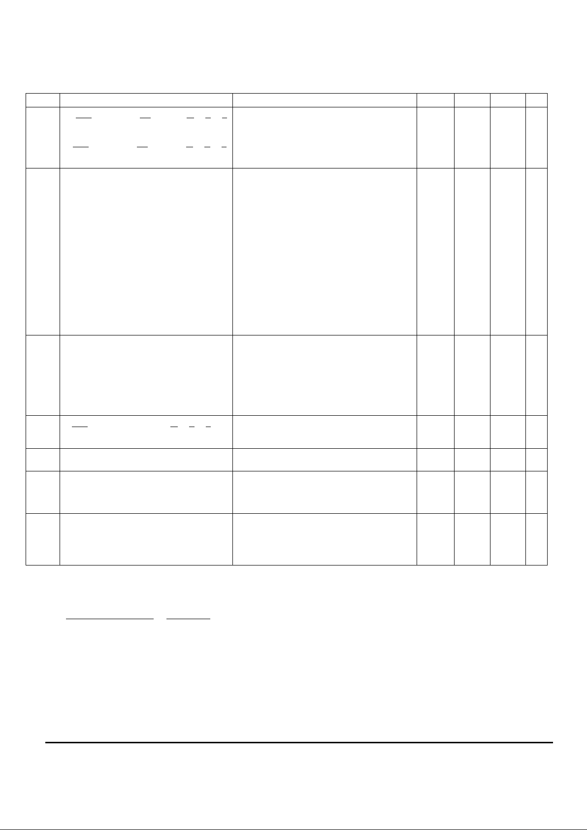
ELECTRICAL CHARACTERISTICS (Voltage Referenced to VSS, VDD=2.4 to 3.5V, TA=25˚C)
Symbol Parameter Test Condition Min Typ Max Unit
DV
DD
AV
DD
Logic Circuit Supply Voltage Range
Voltage Generator Circuit Supply Voltage Range
(Absolute value referenced to VSS) 2.4
2.4
3.0
-
3.5
3.5
V
V
I
AC
I
DP
I
SB
I
ICON
Access Mode Supply Current Drain
(AVDD + DVDD Pins)
Display Mode Supply Current Drain
(AVDD + DVDD Pins)
Standby Mode Supply Current Drain
(AVDD + DVDD Pins)
Icon Mode Supply Current Drain
(AVDD + DVDD Pins)
VDD=3.0V, Internal DC/DC Converter On, 5X DC/DC
Converter Enabled, R/W accessing, T
cyc
=1MHz,
Osc. Freq.=50KHz, Display On.
VDD=3.0V, Internal DC/DC Converter On, 5X Converter Enabled, R/W Halt, Osc. Freq.=50KHz, Display On.
VDD=3.0V, Display off, Oscillator Disabled, R/W halt.
VDD=3.0V, Internal Oscillator, Oscillator Enabled,
Display On, Icon On, R/W halt, Freq.=50KHz.
-
-
-
-
500
300
TBD
TBD
TBD
TBD
1
25
µA
µA
µA
µA
V
CC
V
LCD
LCD Driving Internal DC/DC Converter Output
(VCC Pin)
LCD Driving Voltage Input (VCC Pin)
Display On, DC/DC Converter Enabled, Osc. Freq.=
50KHz, Internal Regulator Enabled, Divider Enabled.
Internal DC/DC Converter Disabled.
7
7
15
15
16.5
16.5VV
V
ICON
Low Power Icon mode Voltage -2-V
V
OH1
V
OL1
V
R1
V
R2
Output High Voltage
(D0-D7, OSC2)
Output Low Voltage
(D0-D7, OSC2)
LCD Driving Voltage Source (VR Pin)
LCD Driving Voltage Source (VR Pin)
I
out
=100µA
I
out
=100µA
Internal Regulator Enabled (VR voltage depends on
Int/Ext Contrast Control)
Internal Regulator Disable.
0.9*V
DD
0
0
-
-
-
-
Floating
V
DD
0.1*V
DD
VCC-0.5
-
V
V
V
V
MOTOROLA
3–282
MC141800A
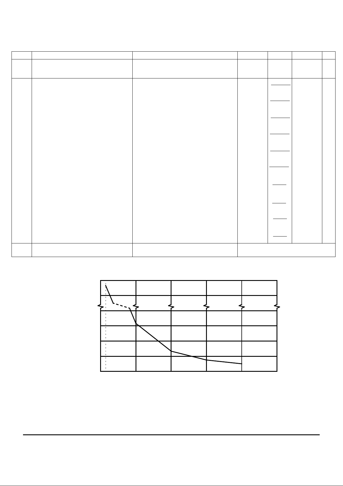
ELECTRICAL CHARACTERISTICS (Voltage Referenced to VSS, VDD=2.4 to 3.5V, TA=25˚C)
* The formula for the temperature coefficient is:
Symbol Parameter Test Condition Min Typ Max Unit
V
IH1
V
IL1
Input high voltage
(RES, OSC2, CLK, CE, D0-D7,R/W, D/C, S/P,
OSC1)
Input Low voltage
(RES, OSC2, CLK, CE, D0-D7, R/W, D/C, S/P,
OSC1)
0.8*V
DD
0
-
-
V
DD
0.2*V
DD
V
V
V
LL6
V
LL5
V
LL4
V
LL3
V
LL2
V
LL6
V
LL5
V
LL4
V
LL3
V
LL2
V
LL6
V
LL5
V
LL4
V
LL3
V
LL2
LCD Display Voltage Output
(V
LL6
, V
LL5
, V
LL4
, V
LL3
, V
LL2
Pins)
LCD Display Voltage Output
(V
LL6
, V
LL5
, V
LL4
, V
LL3
, V
LL2
Pins)
LCD Display Voltage Input
(V
LL6
, V
LL5
, V
LL4
, V
LL3
, V
LL2
Pins)
Smart Bias Divider Enabled, 1:9 bias ratio
Smart Bias Divider Enabled, 1:7 bias ratio
External Voltage Generator, Smart Bias Divider Disable
-
-
-
-
-
-
-
-
-
-
7
0
0
0
0
V
R
8/9*V
R
7/9*V
R
2/9*V
R
1/9*V
R
V
R
6/7*V
R
5/7*V
R
2/7*V
R
1/7*V
R
-
-
-
-
-
-
-
-
-
-
-
-
-
-
-
V
CC
V
LL6
V
LL5
V
LL4
V
LL3
V
V
V
V
V
V
V
V
V
V
V
V
V
V
V
I
OH
I
OL
I
OZ
Output High Current Source
(D0-D7, OSC2)
Output Low Current Drain
(D0-D7, OSC2)
Output Tri-state Current Drain Source
(D0-D7, OSC2)
V
out=VDD
-0.4V
V
out
=0.4V
50
-
-1
-
-
-
-
-50
1
µA
µA
µA
IIL/IIHInput Current
(RES, OSC2, CLK, D0-D7, R/W, D/C, S/P,
OSC1)
-1 - 1 µA
C
IN
Input Capacitance
(OSC1, OSC2, all logic pins)
- 5 7.5 pF
V
CN
Internal Contrast Control
(VR Output Voltage)
Internal Regulator Enabled, Internal Contrast control
Enabled. (16 Voltage Levels Controlled by Software.
Each level is typically 1.5% of the Internal Regulator
Output Voltage.)
- ± 12 - %
PTC0
PTC1
PTC2
PTC3
Temperature Coefficient Compensation
Flat Temperature Coefficient
Temperature Coefficient 1*
Temperature Coefficient 2*
Temperature Coefficient 3*
(TC1=0, TC2=0, Internal Regulator Disabled.)
(TC1=0, TC2=1, Internal Regulator Enabled.)
(TC1=1, TC2=0, Internal Regulator Enabled.)
(TC1=1, TC2=1, Internal Regulator Enabled.)
-
-
-
-
0.0
-0.18
-0.22
-0.35
-
-
-
-
%
%
%
%
TC(%)=
VR at 50˚C - VR at 0˚C
50˚C - 0˚C
X
1
VR at 25˚C
X100%
3–283
MC141800AMOTOROLA
Figure 1. Internal Oscillator Frequency Relationship with External Resistor Value
AC ELECTRICAL CHARACTERISTICS (TA=25˚C, Voltage referenced to VSS, AVDD=DVDD=3V)
Symbol Parameter Test Condition Min Typ Max Unit
F
OSC
Oscillation Frequency of Display timing generator 60Hz Frame Frequency
Either External Clock Input or Internal Oscillator
Enabled
45 60 55 KHz
F
FRM
Frame Frequency Graphic Display Mode, Normal Frequency Mode,
65 - 49 MUX
Graphic Display Mode, Half Frequency Mode,
65 - 49 MUX
Graphic Display Mode, Normal Frequency Mode,
48 - 33 MUX
Graphic Display Mode, Half Frequency Mode,
48 - 33 MUX
Graphic Display Mode, Normal Frequency Mode,
32 - 2 MUX
Graphic Display Mode, Half Frequency Mode,
32 -2 MUX
6-Phase Low Power Icon Mode, Normal Frequency
Mode
6-Phase Low Power Icon Mode, Half Frequency
Mode
4-Phase Low Power Icon Mode, Normal Frequency
Mode
4-Phase Low Power Icon Mode, Half Frequency
Mode
-
-
-
-
-
-
-
-
-
-
-
-
-
-
-
-
-
-
-
-
Hz
Hz
Hz
Hz
Hz
Hz
Hz
Hz
Hz
Hz
OSC Internal Oscillation Frequency with different value
of feedback resistor
Internal Oscillator Enabled, VDD within operation
range
See Figure 1 for the relationship
F
OSC
15 * MUX
F
OSC
960
F
OSC
1920
F
OSC
1024
F
OSC
2048
F
OSC
30 * MUX
F
OSC
23 * MUX
F
OSC
46 * MUX
F
OSC
30 * MUX
F
OSC
60 * MUX
100k 500k 1.0M 1.5M 2.0M
Resistor Value between OSC1 and OSC2 (Ω)
Oscillation
Frequency
(Hz)
260k
90k
70k
50k
30k
10k
280k

MOTOROLA
3–284
MC141800A
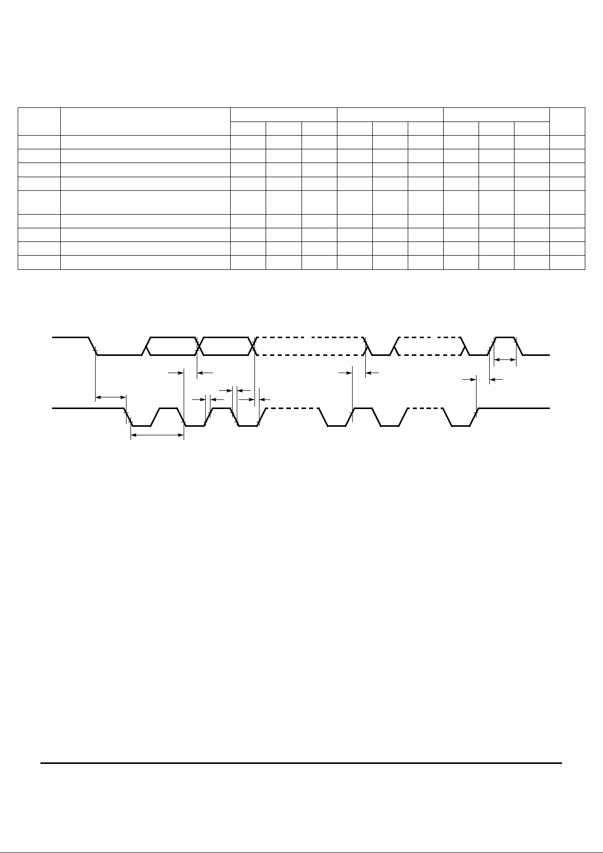
TABLE 3. Parallel Timing Characteristics (TA=-30 to 85˚C, DVDD=2.4 to 3.5V, VSS=0V)
Symbol Parameter Min Typ Max Unit
t
cycle
Clock Cycle Time 1000 - - ns
t
AS
Address Setup Time 90 - - ns
t
AH
Address Hold Time 60 - - ns
t
DSW
Write Data Setup Time 210 - - ns
t
DHW
Write Data Hold Time 75 - - ns
t
DSR
Read Data Setup Time 250 - - ns
t
DHR
Read Data Hold Time 75 - - ns
t
ACC
Access Time - - 250 ns
PW
EL
Enable Low Pulse Width 390 - - ns
PW
EH
Enable High Pulse Width 390 - - ns
t
R
Rise Time - - 45 ns
t
F
Fall Time - - 45 ns
Valid Data
t
cycle
t
DSW
t
AS
t
AH
t
DHR
t
ACC
CLK
D/
C
D0-D7
CE
Valid Data
D0-D7
(Write data to driver)
(Read data from driver)
t
DHW
PW
EH
PW
EL
t
R
t
F
t
DSR
R/W
Figure 2. Parallel 6800-series Interface Timing Characteristics
3–285
MC141800AMOTOROLA
TABLE 4. IIC Serial Timing Characteristics (TA=-30 to 85˚C, DVDD=2.4 to 3.5V, VSS=0V)
Symbol Parameter
100kHz 400kHz 1MHz
Unit
Min Typ Max Min Typ Max Min Typ Max
t
cycle
Clock Cycle Time 10 - - 2.5 - - 1 - - µs
t
HSTART
Start condition Hold Time 4.0 - - 0.6 - - 0.3 - - µs
t
HD
Data Hold Time 500 - - 300 - - 150 - - ns
t
SD
Data Setup Time 250 - - 100 - - 50 - - ns
t
SSTART
Start condition Setup Time (Only relevant for a
repeated Start condition)
4.7 - - 0.6 - - 0.3 - - µs
t
SSTOP
Stop condition Setup Time 4.0 - - 0.6 - - 0.3 - - µs
t
R
Rise Time for data and clock pin - - 1000 - - 300 - - 150 ns
t
F
Fall Time for data and clock pin - - 300 - - 300 - - 150 ns
t
IDLE
Idle Time before a new transmission can start 4.7 - - 1.3 - - 0.6 - - µs
Figure 3. IIC Serial Interface Timing Characteristics
CLK
SDA
t
cycle
t
HSTART
t
HD
t
IDLE
t
SSTOP
t
F
t
R
t
SSTART
()(
)
()(
)
t
SD
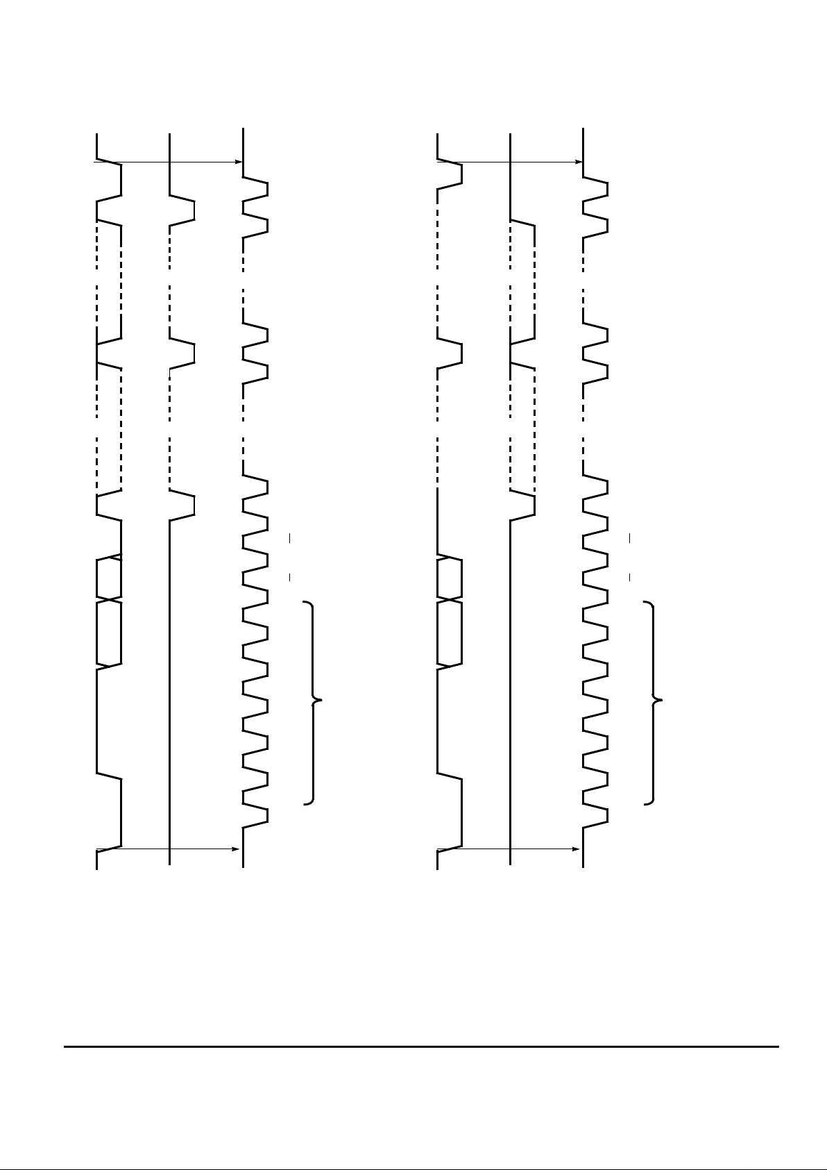
MOTOROLA
3–286
MC141800A
Figure 4. IIC Serial Interface Input Protocol (Write Data to Driver)
Figure 5. IIC Serial Interface Output Protocol (Read Data from Driver)
ADDRESS
D/
CR/W
ACK
STOP
CONDITION
DATA
ACK
ACK
1 - 8
9
P
(
)
(
)
(
)
(
)
(
)
(
)
1
CLK
SDA
START
CONDITION
S
(From controller)
SDA
(From Driver)
A1
A2
(
)
(
)
(
)
(
)
(
)
(
)
(A0)
23456789
ADDRESS
D/
CR/W
ACK
STOP
CONDITION
DATA
ACK
ACK
1 - 8
9
P
(
)
(
)
(
)
(
)
(
)
(
)
1
CLK
SDA
START
CONDITION
S
(From controller)
SDA
(From Driver)
A1
A2
(
)
(
)
(
)
(
)
(
)
(
)
(A0)
23456789
 Loading...