

Page 1

Integrated Information S ys tem s Group
8201 E. McDowell Road
Scottsdale, AZ 85252-1417
Exhibit 8 – Users Manual
Card Acceptance Device (CAD+)
Low Power Transceiver Module
FCC ID: ABZMCAD200
Model Nos. T6480A
(and variants)
8.0 Card Acceptance Device (CAD+) Use rs Manual
Exhibit 8
Page 1 of 113 FCC ID: ABZMCAD200
10/10/00
Page 2

MCAD 200
CARD ACCEPTANCE DEVICE (CAD+)
Models
T6479A (Parallel)
T6480A (Serial)
T6481A (Serial)
T6499A (Serial)
T6500A (Serial)
T6501A (Serial)
T6548A (Serial)
Instruction Manual
68P81131E43-O
*6881131e43*
Page 3

MOTOROLA READER WARRANTY
Warranty: Motorola, Inc. (Motorola") warrants its Motorola manufactured smartcard reader or terminal (Prod
uct") to the original purchaser (Buyer") as stated herein, except to the extent the terms herein may be modified by a
written SmartCard Systems Agreement between Motorola and Buyer. Smartcards are not covered by this warranty.
Motorola warrants the Product against material defects in material and workmanship under normal use and service
for a period of One (1) Year from the date of Product shipment. Motorola, at its option, will at no charge either repair
the Product (with new or reconditioned parts), replace it with the same or equivalent product (using new or recondi
tioned parts), or refund the purchase price of the Product during the warranty period provided Buyer notifies Moto
rola within the warranty period in accordance with the terms of this warranty. Repaired or replaced product is war
ranted for the balance of the original applicable warranty period. All replaced parts of the Product shall become the
property of Motorola.
Warranty Exclusions: This warranty does NOT cover:
1. Defects, damage or malfunctions of the Product resulting from:
(a) Use of the Product in other than its normal and customary manner.
(b) Misuse, accident, neglect, environmental or site conditions not conforming to the Product specifications.
(c) Alteration, modification, adjustment, repair or testing of the Product not approved by Motorola.
(d) Equipment not approved by Motorola for use with the Product.
(e) Excessive power conducted or radiated from equipment not approved by Motorola for use with the Prod
uct.
2. Product which has had the serial number removed or made illegible.
3. Normal and customary wear and tear.
4. Fraud, theft or loss resulting from unauthorized use of the Product.
5. Loss of value or data stored in the Product or in other equipment used with the Product.
6. Disclosure of personal or confidential information or data stored in or accessed by the Product.
7. Loss or damage from Product or system downtime.
8. Scratches or other cosmetic damage to Product surfaces that does not affect the operation of the Product.
9. That the software in the Product will meet the purchaser's requirements or that the operation of the software will
be uninterrupted or error-free.
General Provisions: This express warranty is extended by Motorola to the original Buyer purchasing the Product,
and is not assignable or transferable to any other party. This is the complete warranty for the Product. Motorola
assumes no obligations or liability for additions or modifications to this warranty unless made in writing and signed
by an officer of Motorola. Unless made in a separate written agreement(s) between Motorola and Buyer, Motorola
does not warrant the maintenance or service of the Products other than stated herein.
Motorola cannot be responsible in any way for any ancillary equipment not furnished by Motorola which is attached
to or used in connection with the Product, or for operation of the Product with any ancillary equipment, and all such
equipment is expressly excluded from this warranty. Because each system which may use the Product is unique,
Motorola disclaims liability for read range, transaction time, or operation of the system as a whole under this warran
ty other than stated above.
This warranty sets forth the full extent of Motorola's responsibilities regarding the Product. Replacement or refund
of the purchase price, at Motorola's option, is the exclusive remedy. THIS WARRANTY IS GIVEN IN LIEU OF ALL
OTHER EXPRESS WARRANTIES. MOTOROLA DISCLAIMS ALL OTHER WARRANTIES OR CONDITIONS, EX
PRESS OR IMPLIED, INCLUDING THE IMPLIED WARRANTIES OR CONDITIONS OF MERCHANTABILITY AND
FITNESS FOR A PARTICULAR PURPOSE. IN NO EVENT SHALL MOTOROLA BE LIABLE FOR DAMAGES IN EX
CESS OF THE PURCHASE PRICE OF THE PRODUCT, FOR ANY LOSS OF USE, LOSS OF TIME, INCONVE
NIENCE, COMMERCIAL LOSS, LOST PROFITS OR SAVINGS OR OTHER INCIDENTAL, SPECIAL, INDIRECT OR
CONSEQUENTIAL DAMAGES ARISING OUT OF THE USE OR INABILITY TO USE SUCH PRODUCT, TO THE FULL
EXTENT SUCH MAY BE DISCLAIMED BY LAW.
Page 4

Patent and Software Provisions: Motorola will defend, at its own expense, any suit brought against the Buyer to
the extent that it is based on a claim that the Product or its parts infringe a United States patent, and Motorola will pay
those costs and damages finally awarded against the Buyer in any such suit which are attributable to any such
claim, but such defense and payments are conditioned on the following:
(a) that Motorola will be notified promptly in writing by Buyer of any notice of such claim;
(b) that Motorola will have sole control of the defense of such suit and all negotiations for its settlement or compro
mise; and
(c) should the Product or its parts become, or in Motorola's opinion be likely to become, the subject of a claim of
infringement of a United States patent, that Buyer will permit Motorola, at its option and expense, either to
procure for Buyer the right to continue using the Product or its parts or to replace or modify the same so that it
becomes non-infringing or to grant Buyer a credit for the Product or its parts as depreciated and accept its
return. The depreciation will be an equal amount per year over the lifetime of the Product or its parts as estab
lished by Motorola.
Motorola will have no liability with respect to any claim of patent infringement which is based upon the combination
of the Product or its parts furnished hereunder with software, apparatus or devices not furnished by Motorola, nor
will Motorola have any liability for the use of ancillary equipment or software not furnished by Motorola which is
attached to or used in connection with the Product. The foregoing states the entire liability of Motorola with respect
to infringement of patents by the Product or any its parts thereof.
Laws in the United States and other countries preserve for Motorola certain exclusive rights for copyrighted Motoro
la software such as the exclusive rights to reproduce in copies and distribute copies of such Motorola software.
Motorola software may be used in only the Product in which the software was originally embodied and such soft
ware in such Product may not be replaced, copied, distributed, modified in any way, or used to produce any deriva
tive thereof. No other use including, without limitation, alteration, modification, reproduction, distribution, or re
verse engineering of such Motorola software or exercise of rights in such Motorola software is permitted. No license
is granted by implication, estoppel or otherwise under Motorola patent rights or copyrights.
Page 5

FCC Compliance Statement
This device complies with Part 15 of the FCC rules. Operation is subject to the following two conditions. (1) This
device may not cause harmful interference. And (2) this device must accept any interference received, including
interference that may cause undesired operation.
This equipment has been tested and found to comply with the radiated limits for a Class B digital device, pursuant to
Part 15 of the FCC Rules. These limits are designed to provide reasonable protection against harmful interference in
a residential installation. This equipment generates, uses and can radiate radio frequency energy and, if not
installed and used in accordance with the instructions, may cause harmful interference to radio communications.
However, there is no guarantee that interference will not occur in a particular installation. If this equipment does
cause harmful interference to radio or television reception, which can be determined by turning the equipment off
and on, the user is encouraged to try to correct the interference by one or more of the following measures:
-- Reorient or relocate the receiving antenna.
-- Increase the separation between the equipment and receiver.
-- Connect the equipment into an outlet on a circuit different from that to which the receiver is connected.
-- Consult the dealer or an experienced radio/TV technician for help.
This device complies with Part 15 of the FCC rules. Operation is subject to the following two conditions: (1) This
device may not cause harmful interference. And (2) this device must accept any interference received, including
interference that may cause undesired operation.
The CAD+ was submitted and a grant of authorization received from the FCC as a modular device under the inten
tional radiator requirements of Part 15, Subpart C.
The party that incorporates this device into their product is responsible for verification of the emissions produced by
the final product and must adhere to the limits specified in the Code of Federal Regulation 47, Part 15, Subpart B.
Furthermore, a label must be applied on the exterior of the final product referring to this enclosed module which
states, Contains FCC ID: ABZMCAD200" or Contains Transmitter Module FCC ID: ABZMCAD200".
Notice: When an AC source is used to supply power to the integrated equipment, the final equipment will also
have to verify compliance with the AC line conducted emissions according to FCC Part 15, Subpart B. If unsatisfac
tory emissions are measured at the fundamental frequency of the CAD+ then a Corcom 2VK1L power line filter may
be used to suppress the lineconducted emissions.
Caution: Any changes or modifications not approved by the party responsible for compliance could void the
user's authority to operate the equipment
CE Compliance Statement
The Motorola MCAD200 is in conformity with all essential requirements of the Radio & Telecommunications Termi
nal Equipment Directive (R&TTE 1999/5/EC). This product has been assessed to the following standards:
EN 300 330
ETSI EN 301 489-1
ETSI EN 301 489-3
EN 60950: 1992 Incl Amdt 1-4, 11
This product is marked with CE 0560 , which signifies conformity with Class II product requirements specified in
the R&TTE directive.
Page 6
MCAD 2000
CARD ACCEPTANCE DEVICE (CAD+)
Foreword iii. . . . . . . . . . . . . . . . . . . . . . . . . . . . . . . . . . . . . . . . . . . . . . . . . . . . . . . . . . . . . . . . . . . . . . . . .
Performance Specifications iv. . . . . . . . . . . . . . . . . . . . . . . . . . . . . . . . . . . . . . . . . . . . . . . . . . . . . . . . .
Description
Product Overview page 2. . . . . . . . . . . . . . . . . . . . . . . . . . . . . . . . . . . . . . . . . . . . . . . . . . . . . . . . . . . . . . . . . . . .
Simplified Block Diagram Theory page 8. . . . . . . . . . . . . . . . . . . . . . . . . . . . . . . . . . . . . . . . . . . . . . . . . . . . . .
Table of Contents
Models
T6479A (Parallel)
T6480A (Serial)
T6481A (Serial)
T6499A (Serial)
T6500A (Serial)
T6501A (Serial)
T6548A (Serial)
chapter
1
Installation
Unpacking and Inspection page 2. . . . . . . . . . . . . . . . . . . . . . . . . . . . . . . . . . . . . . . . . . . . . . . . . . . . . . . . . . . .
Verifying Proper Operation page 4. . . . . . . . . . . . . . . . . . . . . . . . . . . . . . . . . . . . . . . . . . . . . . . . . . . . . . . . . . . .
Tuning Procedure page 11. . . . . . . . . . . . . . . . . . . . . . . . . . . . . . . . . . . . . . . . . . . . . . . . . . . . . . . . . . . . . . . . . . .
Installing CAD into Terminal page 20. . . . . . . . . . . . . . . . . . . . . . . . . . . . . . . . . . . . . . . . . . . . . . . . . . . . . . . . .
Final Checkout Procedure page 22. . . . . . . . . . . . . . . . . . . . . . . . . . . . . . . . . . . . . . . . . . . . . . . . . . . . . . . . . . .
Troubleshooting
Fault Isolation Procedures page 2. . . . . . . . . . . . . . . . . . . . . . . . . . . . . . . . . . . . . . . . . . . . . . . . . . . . . . . . . . . .
Returning Faulty CADs to Motorola page 3. . . . . . . . . . . . . . . . . . . . . . . . . . . . . . . . . . . . . . . . . . . . . . . . . . . .
Functional Theory of Operation
Functional Theory of Operation page 2. . . . . . . . . . . . . . . . . . . . . . . . . . . . . . . . . . . . . . . . . . . . . . . . . . . . . . .
chapter
2
chapter
3
chapter
4
Motorola, Inc. 2000
All Rights Reserved
Printed in U.S.A.
Worldwide Smartcard
Solutions Division
1301 E. Algonquin Road, Schaumburg, IL 60196
68P81131E43-O
October 15, 2000-eDOC
Page 7

Table of Contents
chapter
CAD Protocols and Commands
TerminaltoCAD Command Protocol page 2. . . . . . . . . . . . . . . . . . . . . . . . . . . . . . . . . . . . . . . . . . . . . . . . . .
Answer to Reset (ATR) page 6. . . . . . . . . . . . . . . . . . . . . . . . . . . . . . . . . . . . . . . . . . . . . . . . . . . . . . . . . . . . . . .
CAD Management Commands page 8. . . . . . . . . . . . . . . . . . . . . . . . . . . . . . . . . . . . . . . . . . . . . . . . . . . . . . . .
Command Sequences page 28. . . . . . . . . . . . . . . . . . . . . . . . . . . . . . . . . . . . . . . . . . . . . . . . . . . . . . . . . . . . . . .
Appendix
Appendix A Performing FLASH Upgrades page A-1. . . . . . . . . . . . . . . . . . . . . . . . . . . . . . . . . . . .
Appendix B CAD Connector PinOuts page B-1. . . . . . . . . . . . . . . . . . . . . . . . . . . . . . . . . . . . . . .
Appendix C Dimensions and Clearances page C-1. . . . . . . . . . . . . . . . . . . . . . . . . . . . . . . . . . . .
Appendix D CAD+ Dip Switch Settings page D-1. . . . . . . . . . . . . . . . . . . . . . . . . . . . . . . . . . . . . .
and MOTOROLA are trademarks of Motorola, Inc.
IBM is a registered trademark of International Business Machines, Inc.
5
ii
October 15, 200068P81131E43-O
Page 8

Product Maintenance
Philosophy
Customer Support
Table of Contents
FOREWORD
Due to the high percentage of surfacemount components and multi
layer circuit board design, the maintenance philosophy for this product
is one of Field Replaceable Unit (FRU) substitution. Each Control
Board and Antenna Board matched set is considered a FRU, and when
determined to be faulty, may be quickly and easily replaced with a
known good set to bring the equipment back to normal operation. The
faulty CAD set must then be shipped to the Motorola Radio Support
Center in Rockford, Illinois for further troubleshooting and repair to the
component level.
Scope of Manual
For complete information on ordering FRU replacement modules, or
instructions on how to return faulty modules for repair, contact the
Motorola System Support Center as follows:
Motorola System Support Center
1311 E. Algonquin Road
Schaumburg, IL 60196
1-800-221-7144
FAX 847-576-2172
Int'l 847-576-7300
This manual is intended for use by experienced technicians familiar
with similar types of equipment. In keeping with the maintenance phi
losophy of Field Replaceable Units (FRU), this manual contains func
tional information sufficient to give service personnel an operational
understanding of all FRU modules, allowing faulty FRU modules to be
identified and replaced with known good FRU replacements.
The information in this manual is current as of the printing date.
Changes which occur after the printing date are incorporated by Stan
dard Manual Revisions (SMR). These SMRs are added to the manuals
as the engineering changes are incorporated into the equipment.
October 15, 2000 68P81131E43-O
iii
Page 9

Table of Contents
PERFORMANCE SPECIFICATIONS
Electrical
Required Supply Voltage 9.0 15.0 V dc; ripple less than 50 mV PP
Maximum 320 mA @ 12 V dc (230 mA typical)
Required Supply Current
Maximum Input Power Requirements 3.6 Watts
CAD PowerUp Time Less than 1 second after power applied
Environmental
Operating Temperature 30 C to +70 C (22 F to +158 F)
Storage Temperature 40 C to +85 C (40 F to +185 F)
Cold and Heat Shock 40 C to +85 C (40 F to +185 F) within 2 hour duration
Vibration
Shock
Bump
Electromagnetic Fields Compliant with ISO 105361, 4.2.8
NoteRatings assume recommended tuning with no metal within 10 cm of an
tenna board
Frequency Range:10 Hz to 500 Hz
Vibration Severity:3 gn
Severity: 60 gn
Duration: 11 msec
Severity: 40 gn
Duration: 6 msec
Number of bumps: 4000
Transmitter
Frequency 13.56 MHz .01%
ISO14443 Type A
Rise/Fall Time: 23 sec rise; <1.5 sec fall
ASK Percentage: 100%
Modulation
ISO14443 Type B
Rise/Fall Time: <2 sec rise and fall
ASK Percentage: 8% to 14%
Receiver
Carrier Frequency 13.56 MHz
Subcarrier Frequency 847.5 kHz
ISO14443 Type A
Modified Manchester
Subcarrier Data
ISO14443 Type B
NRZL BPSK
iv
October 15, 200068P81131E43-O
Page 10

Operational
Serial
CADtoTerminal Communication Protocols
CADtoTerminal Communication Rates
CADtoCard Communication Rate 105.9375 Kbps
CADtoCard Operating Radio Frequency 13.56 MHz
RS232, RS485, and CMOS (depending on model)
Parallel
ByteWide Parallel Transfer
Serial
9600 bps, 19.2 bps, 38.4 Kbps, 57.6 Kbps, and 115.2 Kbps
Parallel
25,000 bytes per second
Table of Contents
October 15, 2000 68P81131E43-O
v
Page 11

Table of Contents
Notes...
vi
October 15, 200068P81131E43-O
Page 12

Chapter 1 Description
chapter contents
Product Overview
Simplified Block Diagram Theory
2
8
Card Acceptance Device (CAD+)
Technical User's Guide
68P81131E43-O
October 15, 2000
Page 13

Card Acceptance Device (CAD+) Technical User's Guide
PRODUCT OVERVIEW
1
The Motorola Card Acceptance Device (CAD) is an electronic module capable of communicating with
ISO 14443 Type A and Type B compatible smart cards via a radio frequency (RF) interface. This
section provides general information about the application and physical properties of the CAD.
Physical Description
Overview
The CAD, which provides the communications interface between a
terminal and customer smart cards, consists of a Control Board and
an Antenna Board. These two boards are connected together by a
100 mm multiconductor interconnect cable. The CAD is connected
to the terminal via a 16pin connector (parallel models) or a 10pin
connector (serial models) located on the Control Board.
Control Board
The Control Board contains a microprocessor, nonvolatile memory,
and radio frequency transmitting and receiving circuitry. This board
communicates with smart cards via an RF link (provided by the
Antenna Board), and to the terminal via RS232, RS485, or CMOS
(serial models) or a bytewide, proprietary parallel (parallel models)
protocol. Note that serial rates range from 9600 bps to 115.2 kbps,
and parallel rates are up to 25 kbytes/sec.
Typical Application
Antenna Board
The Antenna Board consists of a printed circuit board with copper
traces forming the transmit and receive antenna. The Antenna
Board may be one of several types, varying in dimensions and
construction (some types are attached to a ferrite plate with a metal
back plate serving as a ground plane).
The CAD described in this manual is a device which allows
communications to contactless smart cards by a host or terminal. It
is suitable for applications such as automated fare collection,
access control, electronic purse, and vending machines.
1-2
68P81131E43-O
October 15, 2000
Page 14
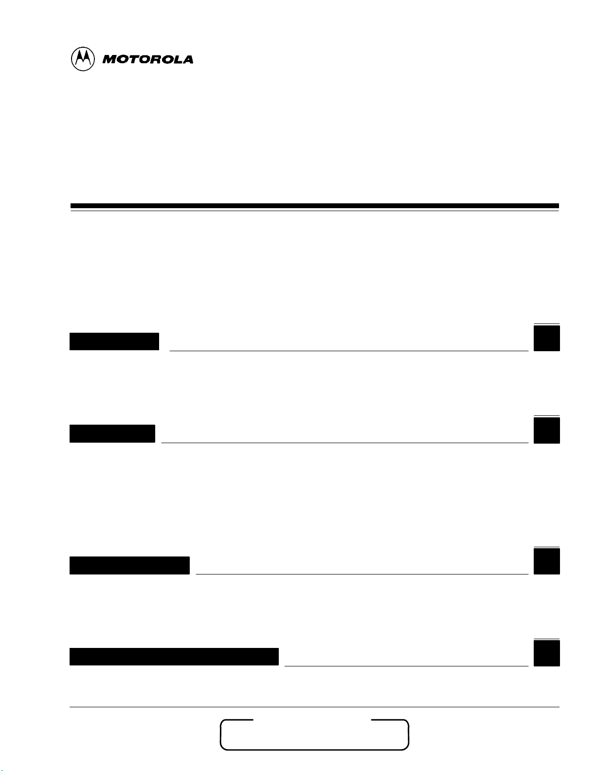
CAD Primary
Components
Chapter 1Description
CONTROL BOARD
ANTENNA BOARD
INTERCONNECT
CABLE
68P81131E43-O
October 15, 2000
1-3
Page 15
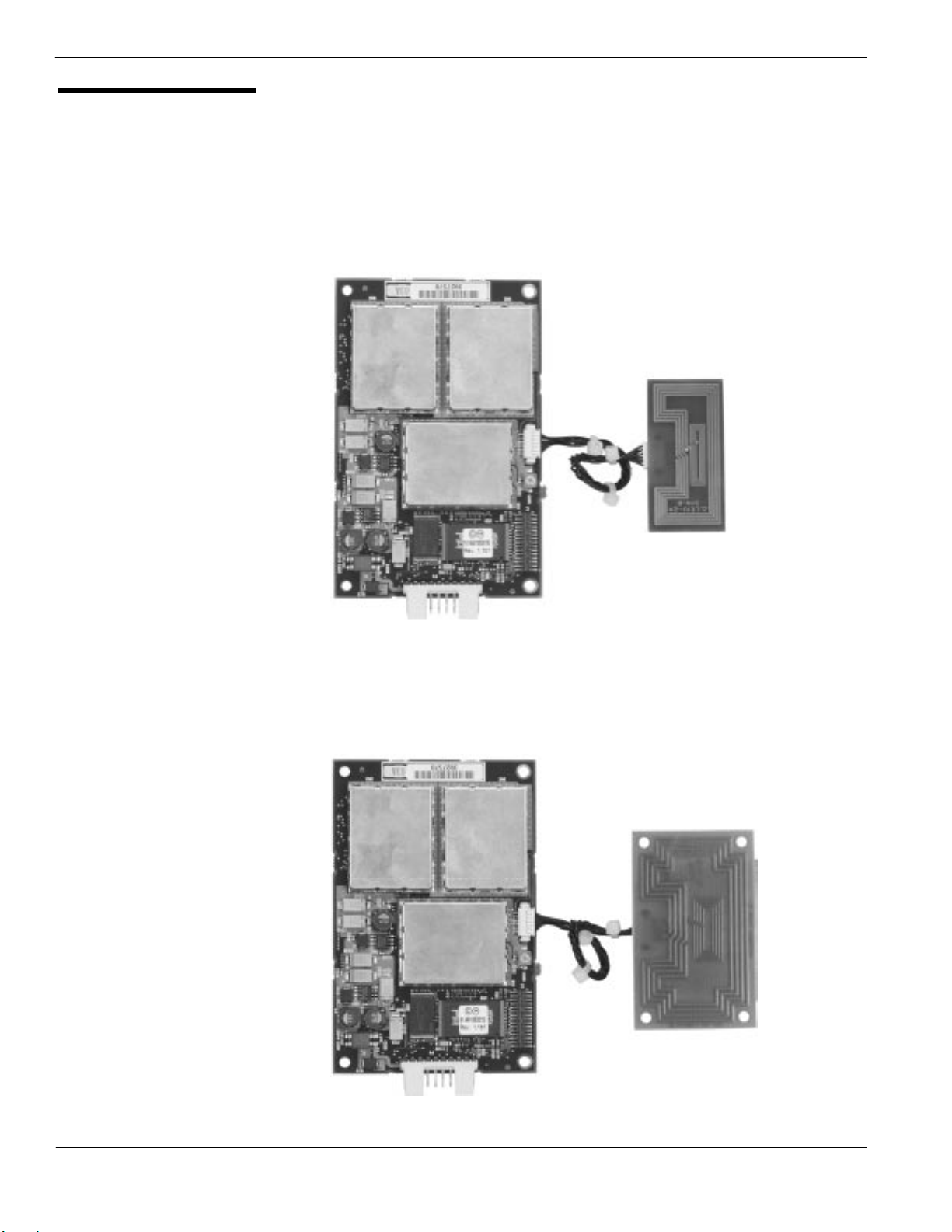
Card Acceptance Device (CAD+) Technical User's Guide
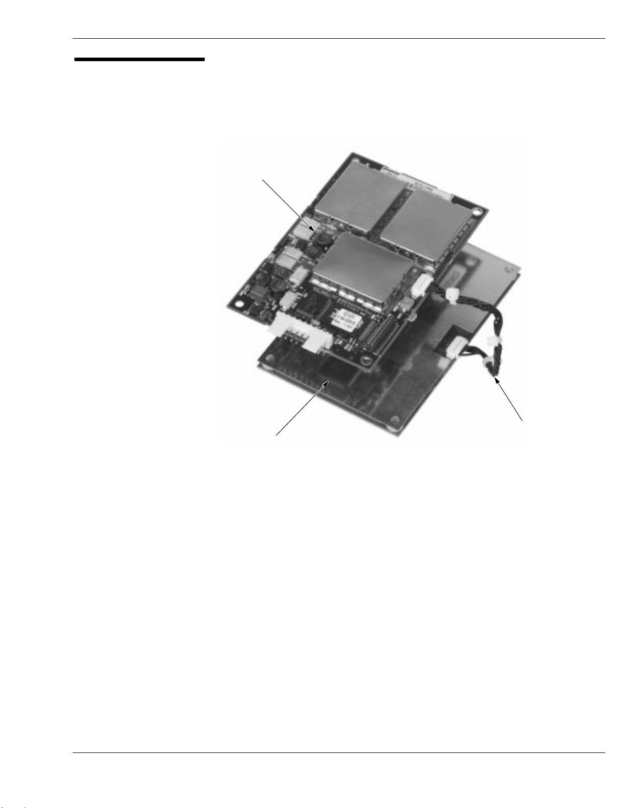
Available Models
The CAD+ is available in several models (shown on the next few
pages). In general, the major differences between the models are
the type of Antenna Board and the type of communications protocol
used to communicate with the terminal.
with Parallel Connector and 104 x 67 mm Antenna Board
Parallel CAD+ (CMOS Interface)
T6480A
T6479A
with Vertical Connector and 104 x 67 mm Antenna Board
Serial CAD+ (RS485 Interface)
1-4
68P81131E43-O
October 15, 2000
Page 16
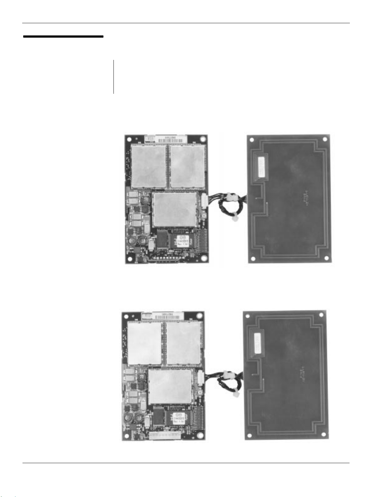
Available Models
(continued)
Chapter 1Description
with Horizontal Connector and 104 x 67 mm Antenna Board
Serial CAD+ (RS485 Interface)
T6481A
with Vertical Connector and 50 x 25 mm Antenna Board
Serial CAD+ (RS485 Interface)
T6499A
68P81131E43-O
October 15, 2000
1-5
Page 17
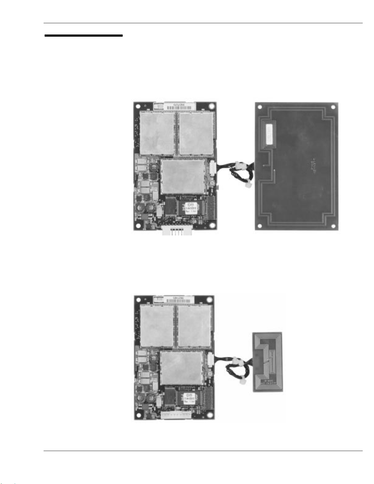
Card Acceptance Device (CAD+) Technical User's Guide
Available Models
(continued)
with Horizontal Connector and 50 x 25 mm Antenna Board
Serial CAD+ (RS485 Interface)
T6500A
with Horizontal Connector and 65 x 40 mm Antenna Board
Serial CAD+ (CMOS Interface)
T6501A
1-6
68P81131E43-O
October 15, 2000
Page 18
Available Models
(continued)
Chapter 1Description
with Vertical Connector and 100 x 110 mm Antenna Board
Serial CAD+ (RS485 Interface)
T6548A
68P81131E43-O
October 15, 2000
1-7
Page 19

Card Acceptance Device (CAD+) Technical User's Guide
2
The illustration on the facing page shows a simplified block diagram of the CAD. This section is
intended to provide a basic understanding of the CAD circuitry and how it interacts with the terminal
and smart cards. (Refer to Chapter 4 for a more detailed block diagram and circuit descriptions.)
SIMPLIFIED BLOCK DIAGRAM THEORY
Overview of CAD
Operation
The CAD serves as the data communications link between a smart
card and the Terminal in which the CAD is installed (or to which the
CAD is connected). The CAD operations are controlled by the
Terminal. The CAD searches (polls) for smart cards within its range,
notifies theTerminal when valid cards are found, and transfers data
from the Terminal to the card, and from the card back to the
Terminal.
For TerminaltoCard communications, the CAD's Control Board
receives a command from the Terminal to transmit data (received
from the Terminal) to the card. The CAD then transmits the data via
modulated encrypted RF signals to the card.
For CardtoTerminal communications, the CAD's Control Board
detects and demodulates encrypted RF data signals from the smart
card and sends data back to the Terminal. Communications with
the Terminal are made using RS485, RS232, or CMOS (serial
models) or 8bit bytewide parallel (parallel models) protocols.
1-8
68P81131E43-O
October 15, 2000
Page 20

CAD Simplified Block
Diagram
Chapter 1Description
CARD ACCEPTANCE DEVICE (CAD)
TERMINAL
SERIAL OR
PARALLEL DATA
(DEPENDING ON
MODEL)
CONTROL BOARD
MICROPROCESSOR
NONVOLATILE
MEMORY
POWER SUPPLY
CIRCUITRY
+5V
+5V_A
100 MM INTERCONNECT CABLE
ANTENNA BOARD
ANALOG
FRONT
END
(AFE)
68P81131E43-O
October 15, 2000
SMART CARD
1-9
Page 21

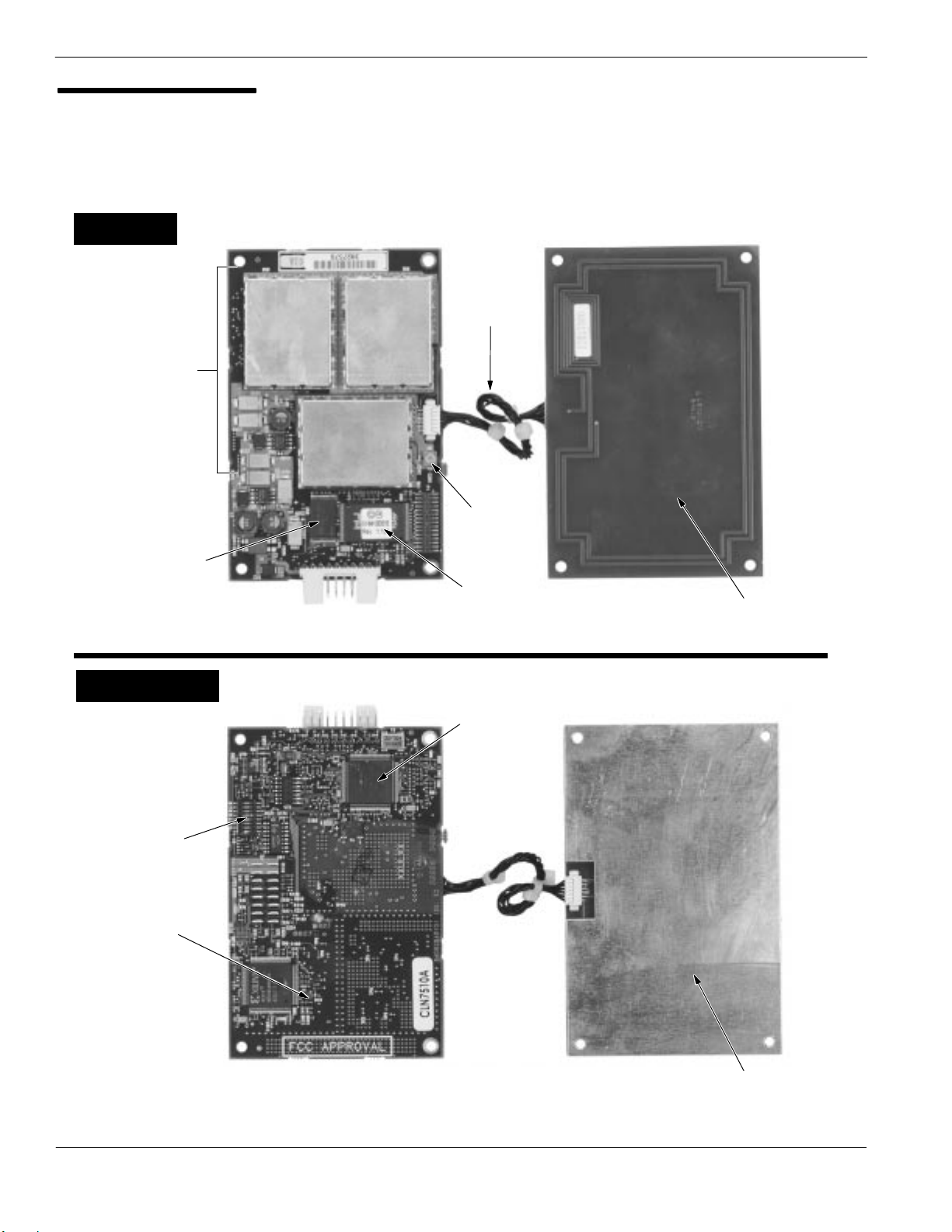
Card Acceptance Device (CAD+) Technical User's Guide
CAD Detailed
Components
The Control Board contains components on both sides of the circuit
board. The Antenna Board contains no components, but rather
printed circuit traces which form the antenna. Refer to the photos
on the next two pages for identification of the components on the
two boards. A typical Parallel CAD
+
and a Serial CAD+ are shown.
1-10
68P81131E43-O
October 15, 2000
Page 22

CAD Detailed
Components
(Typical Parallel CAD+)
Chapter 1Description
TOP VIEW
P/O
ANALOG
FRONT END
(AFE)
BOTTOM VIEW
SRAM
MEMORY
CONTROL BOARD
INTERCONNECT
CABLE
TUNING
CAPACITOR
FLASH
MEMORY
CONTROL BOARD ANTENNA BOARD
MICROPROCESSOR
ANTENNA BOARD
METAL BACK PLATE
(GROUND PLANE)
8POSITION
DIP SWITCH
PARALLEL
CONNECTOR
TO/FROM
TERMINAL
STATUS
(GREEN)
68P81131E43-O
October 15, 2000
LED
ANTENNA CIRCUIT BOARD
(TRACES FORM ANTENNA)
1-11
Page 23
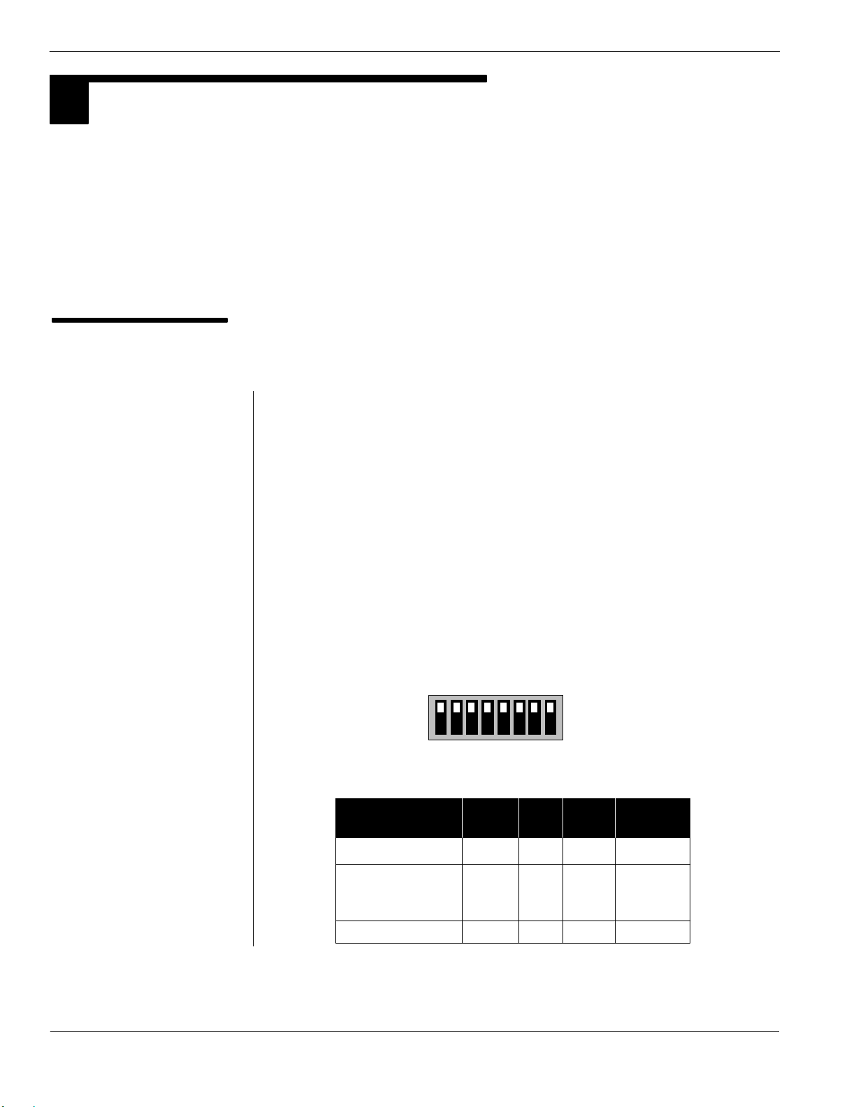
Card Acceptance Device (CAD+) Technical User's Guide
CAD Detailed
Components
(Typical Serial CAD+)
TOP VIEW
P/O
ANALOG
FRONT END
(AFE)
MEMORY
SRAM
CONTROL BOARD ANTENNA BOARD
INTERCONNECT
CABLE
TUNING
CAPACITOR
FLASH
CONNECTS TO
TERMINAL
MEMORY
ANTENNA CIRCUIT BOARD
(TRACES FORM ANTENNA)
BOTTOM VIEW
8POSITION
DIP SWITCH
STATUS
LED
(GREEN)
CONTROL BOARD ANTENNA BOARD
MICROPROCESSOR
METAL BACK PLATE
(GROUND PLANE)
1-12
68P81131E43-O
October 15, 2000
Page 24

Chapter 2 Installation
chapter contents
Unpacking and Inspection
Verifying Proper Operation
Tuning Procedure
Installing CAD Into Terminal
Final Checkout Procedure
2
4
11
20
22
Card Acceptance Device (CAD+)
Technical User's Guide
68P81131E43-O
October 15, 2000
Page 25
Card Acceptance Device (CAD+) Technical User's Guide
UNPACKING AND INSPECTION
1
This section describes the procedures necessary to unpack and take inventory, run a Self Test utility to
verify proper electrical operation, perform a tuning procedure, mechanically install the CAD set into an
external terminal enclosure, and perform a final checkout procedure.
Important!The CAD Control Board contains CMOS and other staticsensitive components. When
handling the CAD, be sure to observe all precautions to prevent damage to the components from static
electricity. These include the use of a grounded antistatic wrist strap and antistatic mats and work
surfaces.
Unpacking and
Inspecting the CAD
Sets
General
Each CAD set (consisting of a Control Board and an Antenna Board) is
tuned and tested at the factory prior to shipment. Each CAD set is
shipped with a 100 mm multiconductor interconnect cable connected
between the Control Board and the Antenna Board.
Remove each CAD set from the packing material and inspect for visual
damage. Report the extent of any damage to the transportation
company and Motorola.
Verifying CAD+ Model Type
Examine the settings on the 8position DIP switch (located on the bottom
of the CAD+ Control Board and compare to the table below to verify the
model type of the CAD+. (Refer to Appendix D for more details on the
DIP switch settings.)
OFF
ON
12345678
CAD+ Model S1 S2 S3 S4-S8
T6479A On Off Off
T6480A, T6481A,
T6499A, T6500A.
T6548A
Off Off Off Off
Off
2-2
T6501A Off On Off Off
68P81131E43-O
October 15, 2000
Page 26

CAD Set Connected by
Cable
MULTICONDUCTOR
INTERCONNECT
CABLE
Chapter 2Installation
ANTENNA
BOARDCONTROL BOARD
68P81131E43-O
October 15, 2000
2-3
Page 27

Card Acceptance Device (CAD+) Technical User's Guide
VERIFYING PROPER OPERATION
2
Although each CAD set is tested at the factory before shipment, it is recommended that the AutoTest
utility be run on each CAD set prior to installation into a terminal. This ensures that the CAD set is
electrically functional and was not electrically damaged in transit or during unpacking.
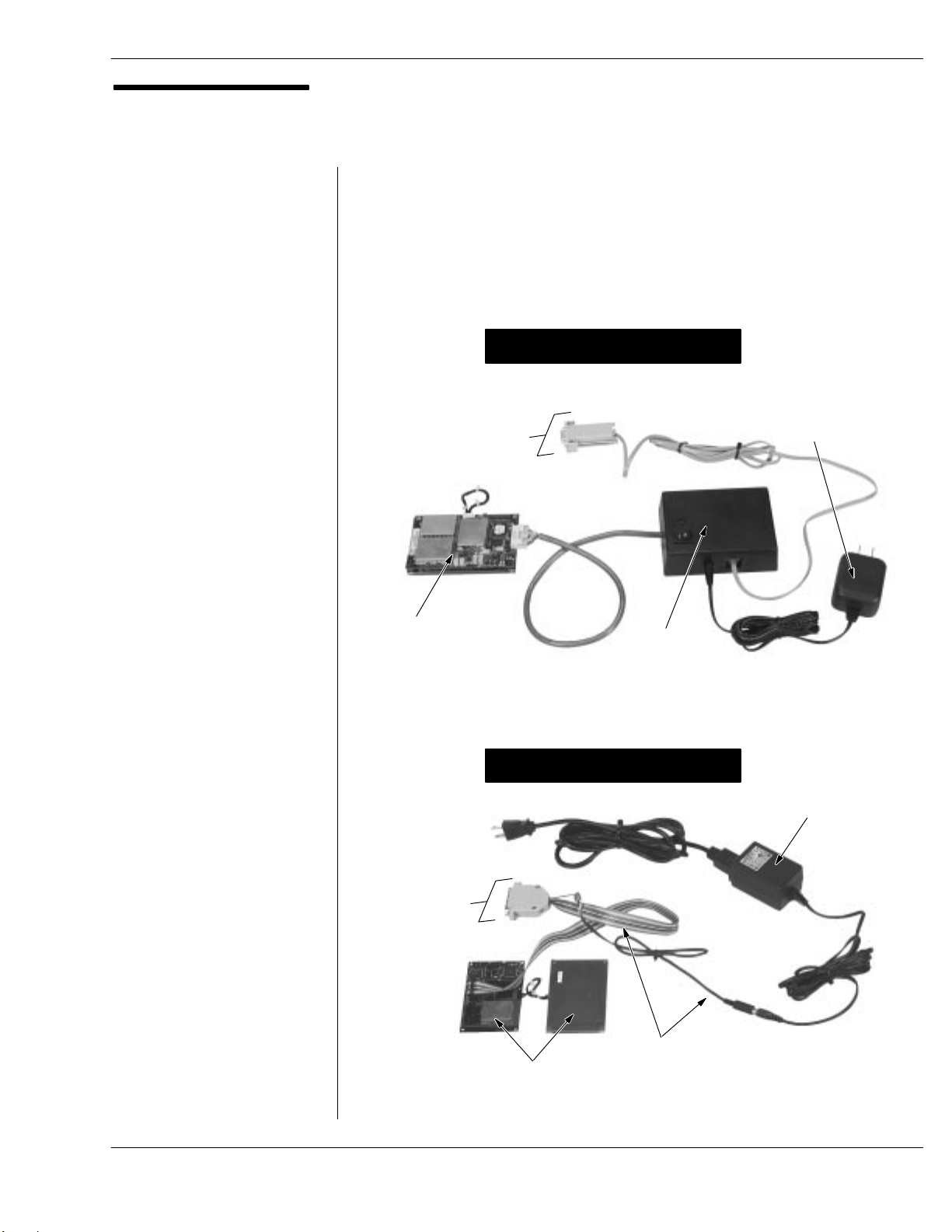
The AutoTest utility is part of the CADTools program included with the Model T6439A Parallel CAD
Installation Kit or the Model T6367A Serial CAD Installation Kit (both available from Motorola). The
CADTools program is a Microsoft Windows compatible program that includes a suite of factory test
utilities and a firmware download utility for updating the CAD operating software.
Required Equipment
The following hardware and software is required in order to run the Self
Test Utility on a CAD set.
Model T6367A Serial CAD Installation Kit includes Serial
Converter Box, Power Supply, ISO Antenna Board, and CADTools
Software (version V1.20 or higher required)
or
Model T6439A Parallel CAD Installation Kit includes Test
Cable, Power Supply, ISO Antenna Board, and CADTools Software
(version V1.20 or higher required)
IBM PC or IBMcompatible desktop or laptop computer (Pentium
II class processor running at 200 MHz or greater, Windows 95, 98,
2000, or NT 4.0 operating system)
Installing the CADTools
Software
2-4
The CADTools software is provided on a CDROM (typically). Install the
software by performing the procedures located in the CADTools User's
Guide (supplied with the software in printed and/or electronic format).
68P81131E43-O
October 15, 2000
Page 28
Launching the
CADTools Software
Chapter 2Installation
1. Before launching the CADTools program, the CAD must be
powered and connected to the PC, as shown below. Make these
connections using the cables and power supply provided in the
Model T6367A (Serial) or T6439A (Parallel) CAD Installation Kit.
Serial CAD Connections
+12 V
CONNECTS TO
COM 1 PORT
ON PC
POWER
SUPPLY
Important!Do not attach or
remove the ribbon cable from the
16pin connector on the Control
Board with DC power on (either
from the Terminal or from the DC
Power Supply included with the
Installation kit). Doing so may result
in corrupted Control Board
firmware.
Important!Make sure that the
PC's parallel port is set for
bidirectional. This setting is
usually provided in the PC's BIOS
setup menu (accessed by pressing
a designated key during the PC's
bootup period).
CAD SET
CONNECTS TO
PARALLEL PORT
ON PC
SERIAL
CONVERTER
BOX
Parallel CAD Connections
TEST CABLE
CAD SET
+12 V
POWER
SUPPLY
68P81131E43-O
October 15, 2000
continued on next page
2-5
Page 29
Card Acceptance Device (CAD+) Technical User's Guide
Launching the
CADTools Software
(continued)
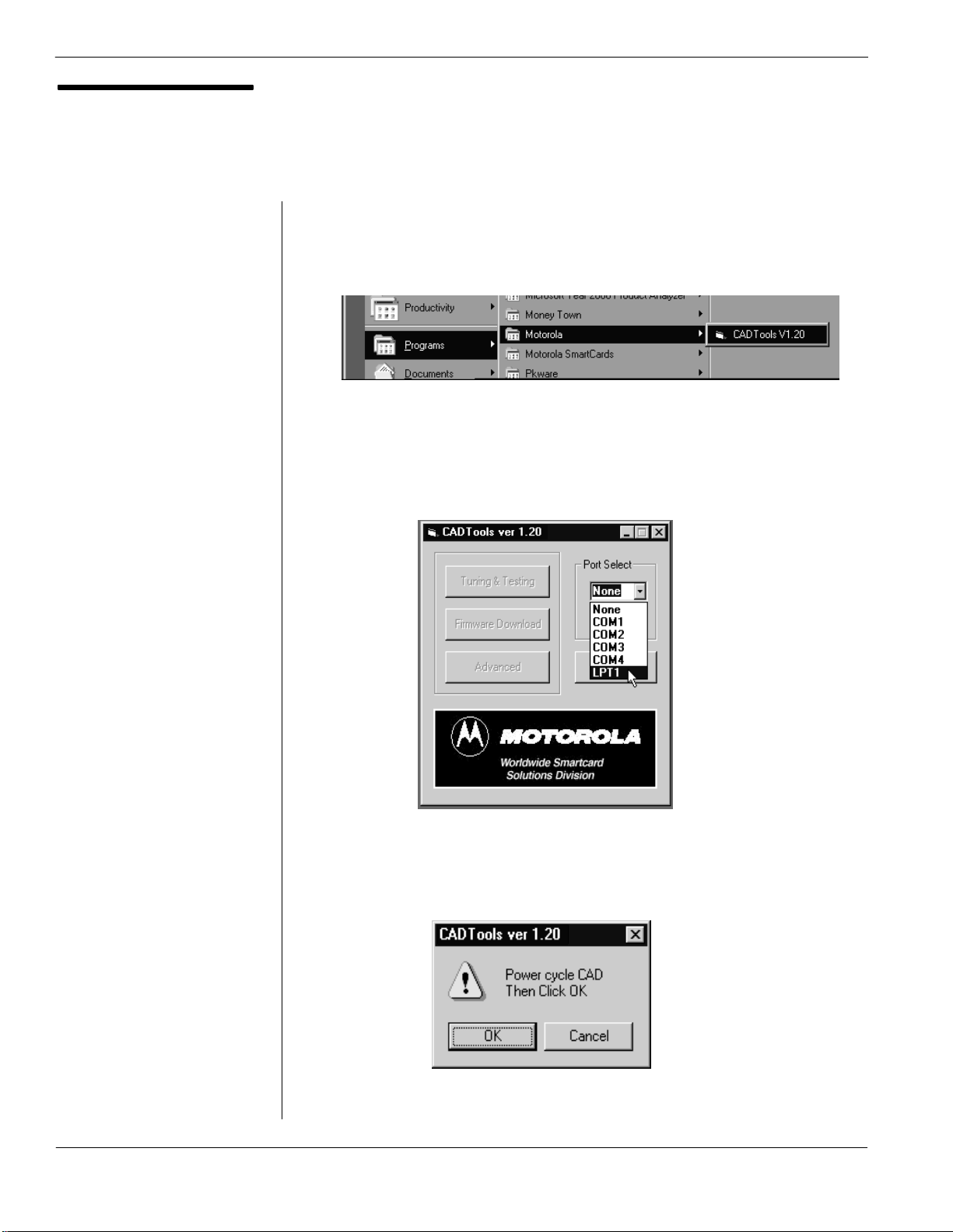
2. Click on the Start button, then select:
Programs ⇒ Motorola ⇒ CADTools
3. The CADTools Main Screen will appear. Click in the Port
Select list box and select COM1 (serial CAD) or LPT1
(parallel CAD). LPT1 is selection is shown below.
2-6
4. The following screen may appear, prompting you to power
cycle the CAD. Disconnect, then reconnect the black DC
power connector to power cycle the CAD. Then click on OK.
continued on next page
68P81131E43-O
October 15, 2000
Page 30
Launching the
CADTools Software
(continued)
Chapter 2Installation
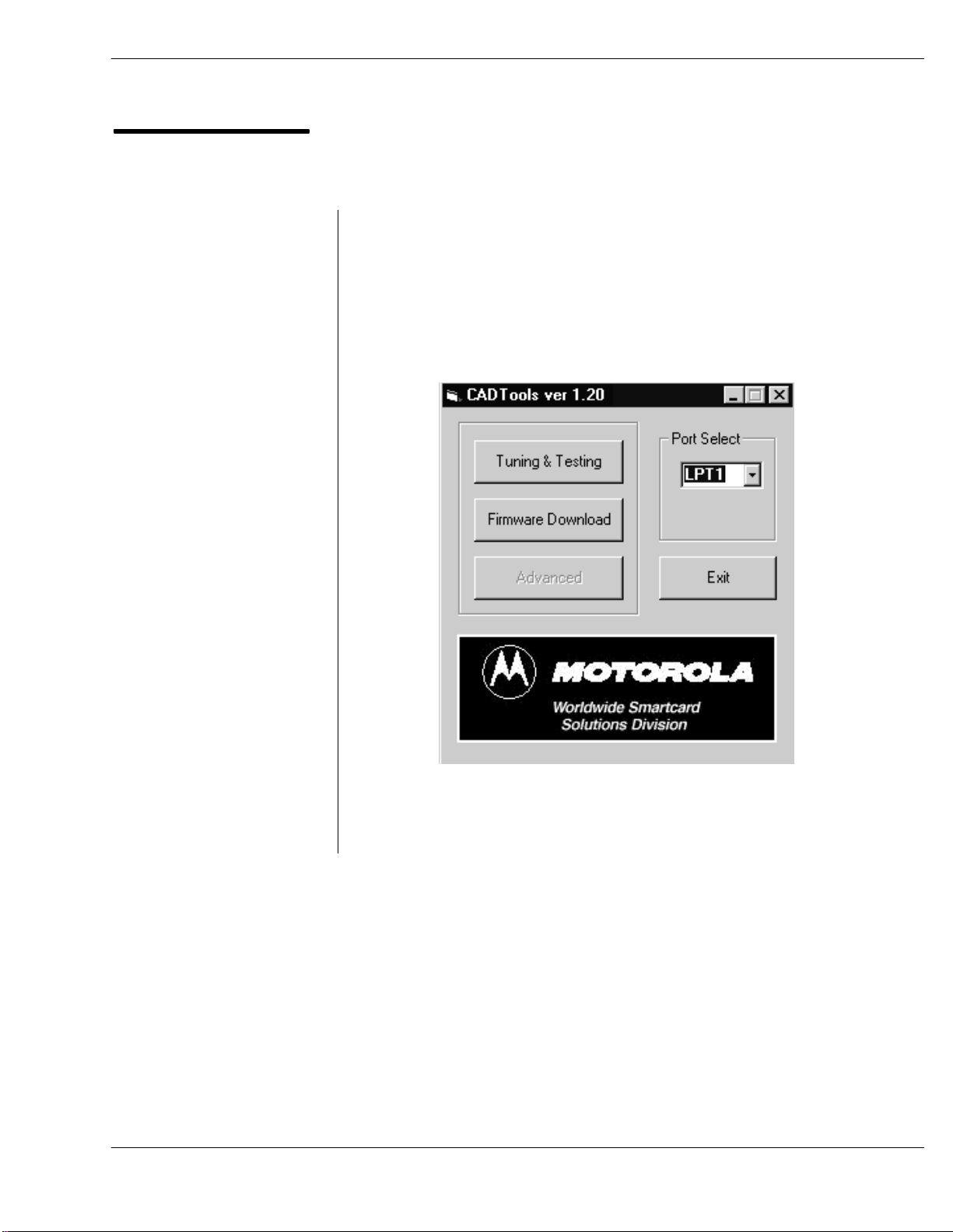
5. The CADTools main screen will appear. It is from this screen that
you can access the Tuning & Testing tool (used to run selftest
diagnostics and perform field tuning) and the Firmware
Download utility (used to download CAD operating software from
the PC into FLASH memory in the CAD Control Board).
68P81131E43-O
October 15, 2000
End of this Procedure
2-7
Page 31

Card Acceptance Device (CAD+) Technical User's Guide
THIS PAGE INTENTIONALLY LEFT BLANK
2-8
68P81131E43-O
October 15, 2000
Page 32

Running the SelfTest
Utility
Chapter 2Installation
1. With the CAD connected to the PC and the CADTools program
running (refer to Launching the CADTools Software on page 2-5),
click on the Tuning & Testing button.
1
2. The following CADTools Tuning & Testing main screen will
appear.
continued on next page
68P81131E43-O
October 15, 2000
2-9
Page 33

Card Acceptance Device (CAD+) Technical User's Guide
Running the Self Test
Utility
(Continued)
3. Click on the Reset CAD button to cause the CAD set to perform
a reboot process. When complete, the Reset command sent
message will be displayed.
Reset command successful
3
4. Click on the AutoTest button to initiate the selftest routine. The
results will be displayed as shown below. Verify that all test
results are OK.
AutoTests Result:
– Flash Checksum: OK
– FPGA load: OK
– UART loopback test: OK
– SRAM test: OK
4
2-10
End of this Procedure
68P81131E43-O
October 15, 2000
Page 34

Chapter 2Installation
TUNING PROCEDURE
3
Introduction
Each CAD set is tuned at the factory for maximum operating range with minimal power. However, in some
cases it may be necessary to tune the CAD set again when it is installed in the terminal due to
characteristics of the terminal (such as metal or metallic paint near the Antenna Board) which can affect
the operating range or reliability. It may also be required to tune the CAD set again if a terminal (such
as a batterypowered terminal) requires minimal power draw from the CAD and a nominal operating
range.
CAD Tuning Guidelines
If the CAD set requires tuning due to Terminal characteristics such as metal or metallic paint near the
Antenna Board (which can affect operating range or reliability), it is recommended that the CAD be
installed into the Terminal first and then tuned. This may require some special adapters (e.g., to connect
the CAD to the PC).
However, there may be situations where tuning the CAD while installed in the Terminal is not possible
(e.g., access to the tuning capacitor is not possible while installed in the Terminal housing). In these
cases, a special tuning fixture" may have to be constructed to simulate the CAD installed in the Terminal
housing while also providing access to the tuning capacitor. The fixture must be constructed so as to
simulate any metal shielding in the Terminal, as well as the precise distance between a presented smart
card and the Antenna Board. For further assistance in constructing a tuning fixture, consult with the
Motorola System Support Center.
If, instead, the Terminal has little or no effect on the CAD performance and the CAD needs to be adjusted,
this can be done prior to installation in the Terminal. In cases such as this, tuning may be performed on
a test bench with the distance between the Antenna Board and the Terminal card presentation target
simulated. The tuning procedure beginning on page 2-12 describes this method.
NoteTo perform the tuning procedure, you will use the CADTools program. This software application
was used previously to perform the SelfTest utility to verify that the CAD is electrically functional. Refer
to page 2-4 for instructions on installing this software application on your PC.
Required Equipment
The following hardware and software is required in order to perform the
tuning procedure on a CAD set.
Model T6367A Serial CAD Installation Kit includes Serial
Converter Box, Power Supply, ISO Antenna Board, and CADTools
Software (version V1.20 or higher required)
or
Model T6439A Parallel CAD Installation Kit includes Test
Cable, Power Supply, ISO Antenna Board, and CADTools Software
(version V1.20 or higher required)
IBM PC or IBMcompatible desktop or laptop computer (Pentium
II class processor running at 200 MHz or greater, Windows 95, 98,
2000, or NT 4.0 operating system)
Oscilloscope (Tek TDS420A, or equivalent)
68P81131E43-O
October 15, 2000
2-11
Page 35

Card Acceptance Device (CAD+) Technical User's Guide
Tuning the CAD
1. Place the Control Board and the Antenna Board on a grounded
antistatic mat as shown below. Because of the metallic content
of the antistatic mat, the CAD Antenna Board must be raised
approximately 5 cm above the mat by using a nonmetallic
spacer (e.g., a few pads of paper).
2. Refer to the photos on page 2-5 to connect the Parallel CAD+
or Serial CAD+ to DC power and the PC. However, make sure
you perform the following substeps in order:
Connect the test cable (supplied in the Installation Kit) to the
CAD and the PC.
Plug the power supply line cord into an AC outlet.
Connect the DC connector from the power supply to the DC
connector on the test cable. The green LED on the Control
Board should light within approximately 1 second.
ANTENNA
BOARD RAISED 5
CM ABOVE MAT
2-12
continued on next page
68P81131E43-O
October 15, 2000
Page 36

Tuning the CAD
(continued)
Chapter 2Installation
3. Place a nonmetallic spacer (e.g., small pad of paper) on top of
the Antenna Board. Note that the pad must be the same
thickness as the distance from the reader surface (target" spot
on the outside of the particular Terminal housing) to the top of
the Antenna Board (where it will be mounted in the Terminal).
PAD OF
PAPER
(OR SIMILAR)
ANTENNA
BOARD
(SHIELDED SIDE)
continued on next page
68P81131E43-O
October 15, 2000
2-13
Page 37

Card Acceptance Device (CAD+) Technical User's Guide
Tuning the CAD
(continued)
4. Attach the scope probe to the ISO Antenna wires and position
the antenna on the spacer, centered over the Antenna Board.
While monitoring the waveform on the oscilloscope, move the
antenna around until you achieve the maximum Vpp reading
(approximately 5 to 10 Vpp). Secure the ISO Antenna in place
using electrical tape or equivalent.
ISO ANTENNA
ATTACH SCOPE PROBE
CONNECTED TO
OSCILLOSCOPE TO
THESE LEADS
2-14
SECURE ANTENNA
USING TAPE
continued on next page
68P81131E43-O
October 15, 2000
Page 38

Tuning the CAD
(continued)
NoteThe Frequency and RSSI
tuning parameters are not used
(and are not adjustable) for CAD+
models.
Chapter 2Installation
5. Launch the CADTools program (described on page 2-5) and
click on the Tuning & Testing button to access the CADTools
Tuning & Testing main screen. The current settings from the CAD
will be retrieved and displayed, as shown below.
6. Locate the tuning capacitor on the CAD Control Board and
adjust it using a plastic tuning tool to achieve the maximum Vpp
reading on the oscilloscope.
Tuning
Capacitor
continued on next page
68P81131E43-O
October 15, 2000
2-15
Page 39

Card Acceptance Device (CAD+) Technical User's Guide
Tuning the CAD
(continued)
7. Click on the up/down arrows in the Antenna adjustment box to
set the RF power to the approximate desired level, as indicated
by the waveform on the oscilloscope. Set to a value of 30 for
minimal power and operating range (as required by some
portable terminals) or a starting value of 220 for maximum
operating range. To adjust for maximum range, continue to
adjust the Antenna value up or down as necessary to obtain the
maximum Vpp reading (not to exceed 10.9 Vpp).
NoteThe table below shows the various CAD+ models and the
Vpp reading you should be able to obtain.
Write down the Vpp reading (label as V max) for use in later
steps. (Always adjust the Antenna value at least one digit from
its starting value to ensure a proper reading on the
oscilloscope.)
Important!Do not place a SmartCard near the antenna board
while making this adjustment.
Maximize
Vpp Reading
(10.9 Vpp max)
Antenna
Board
Size
100 x 110 mm 7.5 Vpp
104 x 67 mm 10.9 Vpp (Note 1)
65 x 40 mm 8.0 Vpp
50 x 25 mm 2.8 Vpp
Note 1Maximum allowable Vpp for any Antenna Board is
10.9 Vpp. Do not exceed this voltage.
Nominal Obtainable Vpp
(max RF power 1 cm
from Antenna)
8. Click on the up/down arrows in the Modulation adjustment box
(to increment/decrement the value one step at at time) to set the
value at a starting value of 165. Change the value (click up once,
then down once) to ensure a proper reading on the oscilloscope.
This value represents an approximate 11% modulation level.
Write down the Vpp reading for use in the next step.
Important!Do not place a SmartCard near the antenna board
while making this adjustment.
2-16
continued on next page
68P81131E43-O
October 15, 2000
Page 40

Tuning the CAD
(continued)
NoteYou can calculate the
Amplitude Modulation percentage
using the following formula:
Chapter 2Installation
9. In the table below, locate the V max voltage (from Step 7) in the
left column and compare the V min voltage (from Step 8) to the
V min values in the corresponding row. The V min voltage from
Step 8 should be between the V min (9%) and V min (13%)
range. If it is not within the range, click on the up/down arrows in
the Modulation adjustment box until the peakpeak voltage of the
CAD is closer to the V min (11%) value.
%AM = 100 *
(V max - V min)
(V max + V min)
V max V min (9%) V min (11%) V min (13%)
11 9.183 8.820 8.469
10.9 9.100 8.740 8.392
10.8 9.017 8.659 8.315
10.7 8.933 8.579 8.238
10.6 8.850 8.499 8.161
10.5 8.766 8.419 8.084
10.4 8.683 8.339 8.007
10.3 8.599 8.259 7.930
10.2 8.516 8.178 7.853
10.1 8.432 8.098 7.776
10 8.349 8.018 7.699
9.9 8.265 7.938 7.622
9.8 8.182 7.858 7.545
9.7 8.098 7.777 7.468
9.6 8.015 7.697 7.391
9.5 7.931 7.617 7.314
9.4 7.848 7.537 7.237
9.3 7.764 7.457 7.160
9.2 7.681 7.377 7.083
9.1 7.597 7.296 7.006
9 7.514 7.216 6.929
8.9 7.430 7.136 6.852
8.8 7.347 7.056 6.775
8.7 7.263 6.976 6.698
8.6 7.180 6.895 6.621
8.5 7.096 6.815 6.544
8.4 7.013 6.735 6.467
8.3 6.929 6.655 6.390
8.2 6.846 6.575 6.313
8.1 6.762 6.495 6.236
8 6.679 6.414 6.159
7.9 6.595 6.334 6.082
7.8 6.512 6.254 6.005
7.7 6.428 6.174 5.928
7.6 6.345 6.094 5.851
7.5 6.261 6.014 5.774
7.4 6.178 5.933 5.697
7.3 6.094 5.853 5.620
7.2 6.011 5.773 5.543
7.1 5.928 5.693 5.466
7 5.844 5.613 5.389
6.9 5.761 5.532 5.312
6.8 5.677 5.452 5.235
6.7 5.594 5.372 5.158
6.6 5.510 5.292 5.081
6.5 5.427 5.212 5.004
6.4 5.343 5.132 4.927
Table Continues on Next Page
68P81131E43-O
October 15, 2000
2-17
Page 41

Card Acceptance Device (CAD+) Technical User's Guide
Tuning the CAD
(continued)
V max V min (9%) V min (11%) V min (13%)
6.3 5.260 5.051 4.850
6.2 5.176 4.971 4.773
6.1 5.093 4.891 4.696
6 5.009 4.811 4.619
5.9 4.926 4.731 4.542
5.8 4.842 4.650 4.465
5.7 4.759 4.570 4.388
5.6 4.675 4.490 4.312
5.5 4.592 4.410 4.235
5.4 4.508 4.330 4.158
5.3 4.425 4.250 4.081
5.2 4.341 4.169 4.004
5.1 4.258 4.089 3.927
5 4.174 4.009 3.850
10. To adjust for operating range, remove the ISO antenna and place
a nonmetallic spacer with the depth of the desired operating
range on the Antenna Board (or Terminal target area if CAD is
installed in the Terminal) and place an initialized compatible
SmartCard on top of the spacer. For example, if the desired
operating range is 5 cm, then place an additional 5 cm spacer
on the Antenna Board (or Terminal target area) and place the
SmartCard on top of it.
NoteThe operating range of a card and CAD depends upon
three primary factors: card type, Antenna Board size, and the RF
power level from the CAD. When adjusting RF power for
operating range, use the following table to determine the typical
maximum range with a given Motorola SmartCard and Antenna
Board. (Note that the ranges shown below are measured from the
surface of the Antenna Board.)
Antenna
Card Operating Range ( 1 cm)
Board
Size MV Series MM Series
100 x 110 mm 7 cm 10 cm
104 x 67 mm 6 cm 9 cm
65 x 40 mm 3 cm 6 cm
50 x 25 mm 2 cm 4 cm
2-18
continued on next page
68P81131E43-O
October 15, 2000
Page 42

Tuning the CAD
(continued)
Chapter 2Installation
11. Click on the RF Loopback Test button and verify the status
shows % of the CAD requests read. If the percentage is 100%,
then proceed to Step 12. Otherwise, increase the RF power by
clicking a few times on the up arrow in the Antenna box. Recheck
the percentage of success by clicking the RF Loopback Test
button again. Repeat this procedure until the status shows 100%
or a maximum is obtained. Proceed to Step 13.
RF Loopback Test
completed successfully
RF Loopback Test:
OK
100% of the CAD requests read
11
12. If the initial success rate is 100%, then continue to adjust the RF
power level down (by clicking on the down arrow in the Antenna
box) a bit and click on the RF Loopback Test button until the
percentage is just less than 100%. Then adjust up a bit until it
shows 100% again. This minimizes the CAD current draw for the
operating range desired.
13. Click on the Save as Defaults button to store the adjustment
settings in FLASH memory on the CAD Control Board.
68P81131E43-O
October 15, 2000
End of this Procedure
2-19
Page 43

Card Acceptance Device (CAD+) Technical User's Guide
INSTALLING CAD INTO TERMINAL
4
The information in this section describes the typical mounting methods for installing a CAD set into a
Terminal.
NoteRefer to Appendix B for pinout details of the CAD connectors, and Appendix C for physical
dimensions and clearances.
Mounting Methods
Introduction
The CAD may be mounted in one of two ways:
Stacked
Separated
Each of these mounting methods is described below.
Stacked" Mounting Method
The Control Board and the Antenna Board have been designed so that
they may be stacked as shown on the facing page. The mounting holes
line up with each other, and may be used with screws and spacers to
secure the CAD to the terminal chassis.
Note that the two boards may be stacked so that the metal shields on the
Control Board are either touching or not touching the metallic surface of
the Antenna Board.
Separated" Mounting Method
The 100 mm cable allows the Control Board and the Antenna Board to
be separated to accommodate various mounting scenarios, as shown
on the facing page.
Other Things You Should Know
The nonmetallic side of the Antenna Board must face towards the
card reading surface of the terminal.
The Antenna Board should be mounted as close as possible to the
Reader target area.
The Antenna Board should be located at least 15 mm (in all
directions) from any metallic materials.
Route the multiconductor interconnect cable away from any
metallic materials. Also, dress and secure cable to prevent
movement.
2-20
68P81131E43-O
October 15, 2000
Page 44

Mounting Methods
Stacked" Mounting Method
CONTROL BOARD
(CONNECTOR SIDE UP)
Chapter 2Installation
ANTENNA BOARD
(METALLIC SIDE UP)
Separated" Mounting Method
68P81131E43-O
October 15, 2000
CONTROL BOARD
ANTENNA BOARD
(NONMETALLIC SIDE FACES TOWARD
CARD READING SURFACE)
2-21
Page 45

Card Acceptance Device (CAD+) Technical User's Guide
5
Once the CAD has been tuned and installed into the terminal, a final checkout procedure must be
performed to ensure that the CAD can communicate with a compatible SmartCard. Once this final
checkout has been performed, the terminal may be placed into service.
FINAL CHECKOUT PROCEDURE
Required Equipment
The following hardware and software is required to perform the final
checkout procedure:
Compatible SmartCard (e.g., Model MV4000D)
Powered terminal with CAD installed
Performing the Final
Checkout Procedure
Place an active SmartCard (one that has been initialized and
personalized for use with the particular terminal application) within
reading distance and verify that the desired results are achieved. For
example, for a transit application, the terminal should generate a receipt
ticket (or some other verification, such as a `'beep" or light, that the
transaction was successful).
2-22
68P81131E43-O
October 15, 2000
Page 46

Chapter 3 Troubleshooting
chapter contents
Fault Isolation Procedures
Returning Faulty CADs to Motorola
2
4
Card Acceptance Device (CAD+)
Technical User's Guide
68P81131E43-O
October 15, 2000
Page 47

Card Acceptance Device (CAD+) Technical User's Guide
FAULT ISOLATION PROCEDURES
1
There are four basic techniques for isolating the CAD as the source of a faulty terminal:
Verify dc power from the terminal (+12 V dc)
Observe LED Indicator on the Control Board
Perform the Self Test diagnostics checkout procedure
Perform the Tuning Procedure
Verify DC Power
With the terminal turned on, the CAD should be receiving
+12 V dc on the following pins:
Parallel CAD+ Pins 1 and 2 of the 16pin parallel
connector located on the Control Board (use pin 3 or
4 as ground)
Verify LED Indicator
Serial CAD+ Pin 3 of the 10pin serial connector
located on the Control Board (use pin 2 as ground)
Verify that the voltage is present using a digital voltmeter. If the
dc voltage is not present:
Make sure the cable from the terminal is securely attached
to the 16pin (parallel) or 10pin (serial) connector on the
Control Board.
Troubleshoot the terminal to determine source of faulty
+12 V dc.
A green LED is provided on the Control Board to provide a visual
indication that the Control board has received dc power and has
successfully performed its startup routine. If this LED is not lit
after applying power:
3-2
Verify +12 V dc power from the terminal (see above)
Reload the CAD operating software into FLASH memory
(refer to Appendix A in this manual)
68P81131E43-O
October 15, 2000
Page 48

Perform the Self Test
Checkout Procedure
Perform the CAD Tuning
Procedure
Chapter 3Troubleshooting
Run the Self Test Utility as described in Chapter 2.
Perform the CAD tuning procedure as described in Chapter 2.
68P81131E43-O
October 15, 2000
3-3
Page 49

Card Acceptance Device (CAD+) Technical User's Guide
RETURNING FAULTY CADS TO MOTOROLA
2
If you have performed the troubleshooting procedures on page 32 and have determined that the CAD
is faulty, the entire CAD (Control Board, Antenna Board, and interconnect cable) must be returned to
Motorola. The faulty CAD will be either repaired or replaced by Motorola service personnel. Contact
the Motorola System Support Center at the contact numbers in the Foreword in this manual for
shipping instructions.
3-4
68P81131E43-O
October 15, 2000
Page 50

Chapter 4 Functional Theory of Operation
chapter contents
Functional Theory of Operation
2
Card Acceptance Device (CAD+)
Technical User's Guide
68P81131E43-O
October 15, 2000
Page 51

Card Acceptance Device (CAD+) Technical User's Guide
1
The following theory of operation describes the operation of the CAD circuitry at a functional level. The information
is presented to give the service technician a basic understanding of the functions performed by the CAD in order
to facilitate fault isolation. Refer to Figure 1 for a block diagram of the CAD.
FUNCTIONAL THEORY OF OPERATION
Microprocessor Circuitry
Overview
The CAD uses a Motorola ColdFire MCF5204 microprocessor (P)
which serves as the main controller for the CAD. The microprocessor,
running at a clock speed of 18.432 MHz (generated by an external
clock circuit) controls the operation of the CAD as determined by the
CAD software contained in the FLASH memory.
Address and Data Buses
The P is equipped with a 32bit address bus used to access the
memory (FLASH and SRAM) and provide control (via memory map
ping) for other circuitry in the CAD. A 16bit data bus is used to transfer
data to/from the P, memory, and the AFE.
Reset Circuit
A Low +5V Detect circuit monitors the level of the +5V supply voltage
and generates a reset signal if it falls below a threshold level. The reset
signal is sent to the P, the I/O Register, the AFE, and FLASH memory.
A hardware reset can also be initiated from both the Serial and Parallel
connectors by applying a low active pulse (1 sec minimum) on the
EXTERNAL_RST# line of either connector.
NonVolatile Memory Circuitry
4-2
FLASH Memory
The CAD software resides in a 256k x 16 FLASH memory IC. The
FLASH memory is accessed by the P via the 32bit Address Bus and
the 16bit Data Bus.
SRAM Memory
To supplement the P's internal 512 bytes of internal SRAM, a 32k x 8
SRAM IC is provided.
68P81131E43-O
October 15, 2000
Page 52

AFE Circuitry
Supply Voltages Circuitry
Chapter 4Functional Theory of Operation
The Analog Front End (AFE) circuitry operates under control of the P
to provide a number of functions, as follows:
Controls the power output to the antenna
Modulates TX data and sends to card (via Antenna Board)
Receives (via Antenna Board) RX data from card and provides
demodulation
The CAD Control Board contains onboard regulators and filtering cir
cuitry to generate the various voltages required by the CAD circuitry.
+12 V from the terminal (via connector P8) is used as the source to
generate +5V and +5V_A supply voltages. Also, the variable PA_PWR
supply voltage is generated and fed to the Power Amplifier (p/o AFE)
to control the RF output power of the CAD.
Antenna Board
Serial Interface Circuitry
The Antenna Board consists of a printed circuit board (with traces that
form the antenna), a ferrite plate (which magnetically shields the anten
na from the Control Board), and a metal back plate (which electrically
shields the antenna from the Control Board). The Antenna Board is
connected to the Control Board by a 6wire cable.
The CAD+ Control Board supports a variety of serial protocols
(RS485, RS232, and CMOS). In order to accomplish this, the Serial
Interface Logic Circuitry routes the desired transmit and receive data
to/from the 10pin Serial Connector as determined by the settings on
an 8position DIP switch located on the board.
68P81131E43-O
October 15, 2000
4-3
Page 53

Card Acceptance Device (CAD+) Technical User's Guide
MICROPROCESSOR CIRCUITRY
+5V
+5V
18.432 MHz
OSCILLATOR
CIRCUITRY
+5V
LOW +5V
DETECT
CLK
MICROPROCESSOR
RESET
EXTERNAL_RST#
RESET
ADDRESS
DATA
TO OTHER
DEVICES
ADDRESS BUS
RS232_TXD
RS232_RXD RS232_RXD
+5V
CS05
AFE_CONTROL
A0-A20
D0-D15
CAD_STRB#
CAD_STRB#
CAD_STRB#
FROM
AFE
RESET
ADDRESS BUS
DATA BUS
I/O
REGISTER
D8-D13
RS232_TXD
AFE_CONTROLS
EXTERNAL_
RST#
SERIAL
CONNECTOR
P/O P4
1
CABLE FROM
D
TO
AFE
A
B
MATES WITH
TERMINAL
NON-VOLATILE MEMORY
+5V
FLASH
A1-A20
RESET
256K X 16
D0-D15
SRAM MEMORY
+5V
SRAM
32K X 8
A0-A14
D8-D15
Figure 1. Card Access Device (CAD) Functional Block Diagram (1 of 3)
4-4
CONNECTOR
CAD W/R#
CAD_ACK#
CAD_STRB#
EXTERNAL_RST#
D0-D7
PARALLEL
P/O P8
14
16
13
15
5
12
MATES WITH
CABLE FROM
TERMINAL
68P81131E43-O
October 15, 2000
Page 54

AFE CIRCUITRY
Chapter 4Functional Theory of Operation
FROM
A
B
+5V_A
AFE_CONTROLS
P
PA_PWR
+5V
CAD READY
INDICATOR
ANTENNA
TO
P
AFE_CONTROL
A0-A3
D8-D15
RESET
ANALOG
FRONT END
(AFE)
ANTENNA_COIL
RECEIVE SIGNAL
6WIRE
CABLE
P6
5
6
3
4
2
1
BOARD
MATES WITH
CABLE FROM
TERMINAL
MATES WITH
CABLE FROM
TERMINAL
PARALLEL
CONNECTOR
P/O P8
+12V
1
2
3
4
SERIAL
CONNECTOR
P/O P4
+12V
3
2
9
SUPPLY VOLTAGES CIRCUITRY
+5V
REGULATOR
Figure 1.Card Access Device (CAD) Functional Block Diagram (2 of 3)
ADJUSTABLE
REGULATOR
FILTER
CIRCUITRY
FILTER
CIRCUITRY
+5V
+5V_A
PA_PWR
68P81131E43-O
October 15, 2000
4-5
Page 55

Card Acceptance Device (CAD+) Technical User's Guide
SERIAL INTERFACE CIRCUITRY
D
RS232_TXD
RS232_RXD
SERIAL INTERFACE
LOGIC CIRCUITRY
(See Note Below)
A
B
C
A
B
C
RS485
RS232
TXA
TXB
RXA
RXB
TXB
RXB
SERIAL
CONNECTOR
P/O P4
7
6
CABLE FROM
5
4
SERIAL
CONNECTOR
P/O P4
8
10
MATES WITH
TERMINAL
MATES WITH
CABLE FROM
TERMINAL
NOTESelection of RS232, RS485, or CMOS Serial Interface is accomplished
by DIP Switch Settings, as follows:
SW1 SW2 SW3 Type of Serial Interface Selected
OFF OFF x RS485 (Selection A Above)
OFF ON ON RS232 (Selection B Above)
OFF ON OFF CMOS (Selection C Above)
Figure 1.Card Access Device (CAD) Functional Block Diagram (3 of 3)
4-6
CMOS
TXB
RXB
SERIAL
CONNECTOR
P/O P4
8
10
68P81131E43-O
October 15, 2000
MATES WITH
CABLE FROM
TERMINAL
Page 56

Chapter 5 CAD Protocols and Commands
chapter contents
TerminaltoCAD Command Protocol
Answer to Reset (ATR)
CAD Management Commands
Command Sequences
2
6
9
28
Card Acceptance Device (CAD+)
Technical User's Guide
68P81131E43-O
October 15, 2000
Page 57

Card Acceptance Device (CAD+) Technical User's Guide
TERMINALTOCAD COMMAND PROTOCOL
1
This section defines the structure of commands initiated by the terminal for transmission control and for
specific control in asynchronous halfduplex transmission protocols. Block protocol type ISO 78163 T=1
is used.
The command structure (shown below) consists of the following blocks:
prologue field
information field
epilogue field
The prologue and epilogue fields are mandatory, and must be sent in every case. The information field
is optional. The number of bytes of the information field is indicated by length (LEN) byte (part of the
prologue field).
Command Structure
Prologue Field Information Field Epilogue Field
NAD PCB LEN Inf EDC
1 Byte 1 Byte 1 Byte 0 to 254 Bytes 2 Bytes
Prologue Field
NAD
The NAD byte in the Prologue field contains the block's target
(DAD) and source (SAD) node addresses, as shown below.
NAD Byte Structure
b8 b7 b6 b5 b4 b3 b2 b1 Meaning
x xx x ---- DAD (Destination Node Address)
----xxxx SAD (Source Node Address)
5-2
68P81131E43-O
October 15, 2000
Page 58

Prologue Field
(continued)
Chapter 5CAD Protocols and Commands
PCB
The PCB byte in the Prologue field serves to control and
supervise the transmission protocol. The PCB byte encodes first
and foremost the block type, as well as supplementary data
needed in this context. The PCB byte information for an Iblock,
an Rblock, and an Sblock are shown below.
PCB Byte Information for an IBlock
b8 b7 b6 b5 b4 b3 b2 b1 Meaning
0 ------- b8=0, Signals Iblock
0 N(S) - 00000 b7=N(S), Send sequence number
0-x00000 b6= Chaining (more data)
PCB Byte Information for an RBlock
b8 b7 b6 b5 b4 b3 b2 b1 Meaning
1 00----- b8=1, Signals Rblock
1 0 0 N(R) ---- b5=N(R), Sequence Number
1 0 0 N(R) 0000 b4b1=0, No errors
1 0 0 N(R) 0001 b4b1=1, EDC or parity error
1 0 0 N(R) 0010 b4b1=2, Other errors
1 0 0 N(R) 0011 b4b1=3, Timeout error
PCB Byte Information for an SBlock
b8 b7 b6 b5 b4 b3 b2 b1 Meaning
1 1------ b8=1 & b7=1, Signals Sblock
1 1000000 RESYNCH req = C0
1 1100000 RESYNCH ans = E0
1 1000010 Abort request = C2
1 1100010 Abort response = E2
1 1000011 WTX request = C3
1 1100011 WTX response = E3
11xxxxxx RFU values used for the CAD manage
ment
68P81131E43-O
October 15, 2000
5-3
Page 59

Card Acceptance Device (CAD+) Technical User's Guide
Information Field (INF)
The presence of INF is optional. When present, INF conveys
either application data in Iblocks for cards, miscellaneous data
for the CAD or nonapplication control and status information in
Sblocks.
In an Sblock, this field is used for the management of the CAD.
The CAD does not support the exhaustive list of SBlocks defined
in ISO 7816-3 T=1. However, the CAD supports Motorola
proprietary definition of SBlocks as commands for
management.
Rblocks do not contain an INF field.
Epilogue Field
This field contains the error detection code (EDC) of the
transmitted block. The protocol definition permits this to be either
an LRC or a CRC. The LRC is calculated as the exclusive OR
(XOR) of all the bytes starting with the NAD through the last byte
of the information field, and is typically referred to simply as the
checksum. For CRC see ISO 3309. The CAD uses the CRC.
5-4
68P81131E43-O
October 15, 2000
Page 60

Chapter 5CAD Protocols and Commands
THIS PAGE INTENTIONALLY LEFT BLANK
68P81131E43-O
October 15, 2000
5-5
Page 61

Card Acceptance Device (CAD+) Technical User's Guide
ANSWER TO RESET (ATR)
2
After cycling the power supply or software reboot, the CAD sends out an ATR. For serial transmission,
the ATR is sent at 9.6 Kbps and then the CAD switches to its programmed baud rate (from 9.6 Kbps to
230.4 Kbps). For parallel transmission, the rate is synchronous. The ATR is a data string, up to 33
bytes long, which contains various data relevant to the transmission protocol and to the card. The
ATR's data string and data elements are defined and described in detail in ISO/IEC 7816-3.
ATR Format
The basic ATR format consists of:
TS one byte, the initial character; specifies the con
ventions to code data bytes in all subsequent charac
ters. There are two possible values of TS (ten consec
utive bits from start to end and corresponding hexade
cimal value). The CAD uses direct convention:
(Z)AZZAZZZAAZ(Z) where logic level ONE is Z (LSB
is first). It equals to "3B" when decoded by direct con
vention.
T0 one byte, the format character; serves to indi
cate the subsequent "interface character" a bit field is
used, from b5 to b8. It further contains the number of
subsequent "historical characters," from b1 to b4.
T0 Byte Information
b8 b7 b6 b5 b4 b3 b2 b1 Meaning
---1 ---- TA1 is transmitted
--1 ----- TB1 is transmitted
- 1------ TC1 is transmitted
1 ------- TD1 is transmitted
----xxxx Number of historical characters
5-6
68P81131E43-O
October 15, 2000
Page 62

ATR Format (continued)
Chapter 5CAD Protocols and Commands
The four least significant bits of any interface byte TDi indicates
a protocol type T, specifying rules to be used to process
transmission protocols. When TD
used. TA
TB1 TC1 and TB2 are the global interface bytes. These
1
is not transmitted, T=0 is
1
global interface bytes shall be interpreted in order to process any
transmission protocol correctly.
The interface characters specify all transmission parameters of
the current protocol. They are constructed from the bytes TAi,
, TCi, and TDi (i =1, 2, 3...). TAi, TBi and TCi indicate the
TB
i
protocol parameters. Their interpretation depends on the
protocol type indicated by T in TD
. TDi indicates the protocol
i-1
type T, as defined in [1] Section 6.1.4.3, and the presence of
subsequent interface characters. The ATR transmission of these
bytes is optional and may be omitted if appropriate.
TDi Byte Information
b8 b7 b6 b5 b4 b3 b2 b1 Meaning
---1 ---- TA
--1 ----- TB
- 1------ TC
1 ------- TD
----xxxx Protocol type for subsequent transmis
When TDi is not transmitted, the default value of TA
TC
is null, indicating that no further interface characters TA
i+1
TB
i+1
TC
i+1
TD
will be transmitted. TA1 to TC3 convey
i+1
is transmitted
i+1
is transmitted
i+1
is transmitted
i+1
is transmitted
i+1
sion
i+1
TB
i+1
i+1
information that shall be used during exchanges between the
terminal and the CAD subsequent to the Answer to Reset. They
indicate the values of the transmission control parameters F, D,
I, P, and N, and the IFSC, block waiting time integer (BWI), and
character waiting time integer (CWI) applicable to T=1 as defined
in ISO/IEC 7816-3. The information contained in TA
to TC1 and
1
TC2 shall apply to all subsequent exchanges.
68P81131E43-O
October 15, 2000
The historical characters, T1 T2 -TK, maximum 15 characters.
It designates general information, for example, the CAD firmware
version.
The value of check character TCK shall be such that the
exclusive-ORing of all bytes from byte T0 to the last byte before
the TCK.
5-7
Page 63

Card Acceptance Device (CAD+) Technical User's Guide
ATR Format (continued)
The structure of the ATR is the initial character TS followed by a
variable number of subsequent characters in the following order:
the format character T0, optionally the interface characters TAi,
TBi, TCi, TDi and optionally the historical characters T1 T2 - TK
and, conditionally, the check character TCK.
Charac
ter
TS 3B Indicates direct convention
T0 F3 F = (1111)
TA
1
TB
1
TC
1
TD
1
TA
2
TD
2
TA
3
TB
3
TC
3
T1
T2
T3
TCK XX LRC used for Check character
ATR Data Information
Value Meaning
, TA1, TB1, TC1, and TD1 present;
bin
3 indicates the number of historical bytes present
71 Most significant half byte (b8 to b5): Default Baud
Rate (0...7)
Least significant half byte (b4 to b1): Di = 1
00 Vpp is not required
FF Indicates amount of extra guard time required
(FF = no guard time)
91 9 = (1001)
, TB2 and TC2 absent; TA2 and TD
bin
present;
1 indicates that T=1 is to be used
81 specific mode" ; [6]
8 = (1000)
, b8 = 1 mode change not allowed
bin
1 indicates that T=1 is to be used
71 7 = (0111)
, TA3, TB3, TC3 present; TD3 absent
bin
1 indicates that T=1 is to be used
FF IFSI = FF, which indicates initial value (255 bytes) for
information field size for the CAD
01 b8-b5 = 0 BWI minimum
b4-b1 = 0 CWI minimum
00 01 = CRC in use
XX
XX
11
Version Number of CAD Firmware (MSB)
Version Number of CAD Firmware (LSB)
NAD used by the CAD
2
5-8
68P81131E43-O
October 15, 2000
Page 64

CAD MANAGEMENT COMMANDS
3
Commands in proprietary SBlocks supported by the CAD are:
RF POWER CONTROL: control of the RF field parameters (page 5-10)
SLEEP: put the CAD in low power mode (page 5-12)
DOWNLOADING: put the CAD in downloading mode (page 5-14)
ERROR REPORT: the CAD indicates an Hardware error (page 5-16)
POLL: put the CAD in card registration mode (page 5-18)
ANSWER TO POLL: the CAD sends the parameters of a card detected (page 5-20)
DETECT CARD: put the CAD in card detection mode (page 5-22)
CARD PRESENCE: the CAD sends to the terminal the result of the DETECT CARD com
mand. (page 5-24)
REBOOT: forces the CAD to reset (page 5-25)
BREAK CHARACTER: forces the CAD to reset (page 5-26)
Chapter 5CAD Protocols and Commands
Commands issued from the Terminal to the CAD are called Requests."
Commands issued from the CAD to the Terminal are called Responses."
68P81131E43-O
October 15, 2000
5-9
Page 65

Card Acceptance Device (CAD+) Technical User's Guide
RF POWER
CONTROL
RF POWER CONTROL request
Description
This command allows the terminal to control the RF field power. The four options
of the PCON byte can turn on the 13.56MHz carrier, turn off the carrier, increase
the power of the RF field and to decrease the power of the RF field.
Direction
Terminal to CAD
Size
6 Bytes
Format
See below
RF POWER CONTROL Request Format
NAD PCB LEN PCON CRC1 CRC2
0x11 0xC5 1 (see below) (see below) (see below)
PCON Values Meaning CRC1 Values CRC2 Values
0x00 Power On 0x3B 0x09
0x01 Power Off 0xB2 0x18
0x02 Decrease Power 0x29 0x2A
0x03 Increase Power 0xA0 0x3B
Other Values Forbidden
5-10
68P81131E43-O
October 15, 2000
Page 66

RF POWER
CONTROL
(continued)
Chapter 5CAD Protocols and Commands
RF POWER CONTROL response
Description
The response frame is an acknowledgement of the previous command,
indicating that the command was properly received and has been executed.
Direction
CAD to Terminal
Size
5 Bytes
Format
See below
RF POWER CONTROL Response Format
NAD PCB LEN CRC1 CRC2
0x11 0xE5 0 0xA4 0x8E
68P81131E43-O
October 15, 2000
5-11
Page 67

Card Acceptance Device (CAD+) Technical User's Guide
SLEEP
SLEEP request
Description
This command switches the CAD board to a lowpower mode. It sequentially
turns off the RF power, stops watchdog timer, unmask only the UART (serial
CAD) or STROBE (parallel CAD) interrupt and switches to the STOP mode of the
ColdFire. While no interrupt from the UART (or STROBE) is received (any frame
from the terminal), the CAD stays in this mode. Any UART (or STROBE) interrupt
wakes the CAD processor core, turns on the RF power and switches to the state
of frame reception.
Direction
Terminal to CAD
Size
5 Bytes
Format
See below
SLEEP Request Format
NAD PCB LEN CRC1 CRC2
0x11 0xC8 0 0xEF 0x1D
SLEEP response
Description
The response frame is an acknowledgment of the previous command that
indicates that the command was properly received and is ready to be executed.
This response is sent before the CAD switches to SLEEP state.
Direction
CAD to Terminal
Size
5 Bytes
5-12
Format
See below
SLEEP Response Format
NAD PCB LEN CRC1 CRC2
0x11 0xE8 0 0xDC 0x3E
68P81131E43-O
October 15, 2000
Page 68

Chapter 5CAD Protocols and Commands
THIS PAGE INTENTIONALLY LEFT BLANK
68P81131E43-O
October 15, 2000
5-13
Page 69

Card Acceptance Device (CAD+) Technical User's Guide
DOWNLOADING
DOWNLOADING request
Description
This command makes the CAD switch to downloading mode. It is only accepted
as the first command after the CAD reboots. The code of the Parameters 1 & 2,
processor and FPGA can be downloaded by selecting the TARGET byte 0x00.
This command must be sent both at the beginning and at the end of the
downloading sequence. At the end of the downloading sequence, this
command confirms that the downloading sequence is correctly complete and
provokes the reset of the CAD processor. The TARGET field of this last block
must be identical to the TARGET field of the previous DOWNLOADING
command.
Direction
Terminal to CAD
Size
6 Bytes
Format
See below
DOWNLOADING Request Format
NAD PCB LEN TARGET CRC1 CRC2
0x11 0xC6 1 (see below) (see below) (see below)
TARGET
Values
0x00 Parameters 12, MCU, and
0x01 All FLASH Code
Note: This is the recommended
Other Values RFU RFU RFU
Meaning CRC1 Values CRC2 Values
0x5F 0xE6
FPGA Code
0xD6 0xF7
(including Boot Block)
download mode
5-14
68P81131E43-O
October 15, 2000
Page 70

DOWNLOADING
(continued)
Chapter 5CAD Protocols and Commands
DOWNLOADING response
Description
The response frame is an acknowledgment of the previous command that
indicates that the command was properly received and is ready to be executed.
Direction
CAD to Terminal
Size
5 Bytes
Format
See below
DOWNLOADING Response Format
NAD PCB LEN CRC1 CRC2
0x11 0xE6 0 0xCC 0xA4
68P81131E43-O
October 15, 2000
5-15
Page 71

Card Acceptance Device (CAD+) Technical User's Guide
ERROR REPORT
ERROR REPORT request
Description
The Terminal sends this command to the CAD to determine if the CAD software
has detected any error during the test sequence at boot up. It is recommended
that the Terminal always issue this command immediately after the CAD boots
and has sent an ATR to ensure the CAD is working properly before further
communications are made.
Direction
Terminal to CAD
Size
5 Bytes
Format
See below
ERROR REPORT Request Format
NAD PCB LEN CRC1 CRC2
0x11 0xE7 0 0x14 0xBD
5-16
68P81131E43-O
October 15, 2000
Page 72

ERROR REPORT
(continued)
Chapter 5CAD Protocols and Commands
ERROR REPORT response
Description
The CAD sends this response after receiving an Error Report Request. The Error
Report Response contains any errors found during the test sequence at boot
up. The tests executed by the CAD at boot-up are the verification of the
processor code checksum, the verification of the FPGA code and a UART test
(serial CAD only) in loopback mode.
Direction
CAD to Terminal
Size
6 Bytes
Format
See below
ERROR REPORT Response Format
NAD PCB LEN ERR CRC1 CRC2
0x11 0xC7 1 (see below) (see below) (see below)
ERR Values Meaning CRC1 Values CRC2 Values
0x00 No Error 0x83 0xBC
0x01 Code Checksum Error 0x0A 0xAD
0x02 FPGA Code Error 0x91 0x9F
0x04 UART Initialization Error
(serial CAD only)
0x08 SRAM Error 0xCB 0x30
Other Values RFU RFU RFU
0xA7 0xFA
68P81131E43-O
October 15, 2000
5-17
Page 73

Card Acceptance Device (CAD+) Technical User's Guide
POLL
POLL request
Description
This command makes the CAD switch to the card detection/anti-collision
sequence. The card must be out of the RF field before sending a Poll request.
The STRAT byte supports two options that order the CAD to detect all cards (Long
Poll) or the first card (Quick Poll) in the RF field.
As the CAD manages the attribution of the NAD for the cards detected in the field,
it reserves NAD values that are already in use and gives free NAD values to a new
card that is detected. But the CAD has no information about the transactions
between the terminal and the card(s). Thus, when the terminal has completed all
the transactions with the card(s) registered, it may indicate to the CAD that the busy
values can be freed or not by setting the appropriate value in the ERASE field.
The TYPE byte of this command indicates to the CAD which type of application
of contactless card in the field must be selected.
Direction
Terminal to CAD
Size
8 Bytes
Format
See below
POLL Request Format
NAD PCB LEN STRAT ERASE TYPE CRC1 CRC2
0x11 0xD0 3 (see
below)
STRAT
Values
0x00 Quick Poll 0x00 Do not erase NAD table
0x01 Long Poll 0x01 Erase NAD table
Other Values RFU Other Values Forbidden
TYPE
Values
0x00 All 0x06 Multimedia
0x01 Transport 0x07 Gaming
0x02 Financial 0x08 Data Storage
0x03 Identification 0x09-0x7E RFU
0x04 Telecommunication 0x7F All previous
0x05 Medical 0x80-0xFF Proprietary
Meaning
Meaning
(see
below)
ERASE
Values
TYPE
Values
(see
below)
xx xx
Meaning
Meaning
5-18
68P81131E43-O
October 15, 2000
Page 74

POLL (continued)
Chapter 5CAD Protocols and Commands
POLL response
Description
The response frame is an acknowledgment of the previous command that
indicates that the command was properly received and is ready to be executed.
Direction
CAD to Terminal
Size
5 Bytes
Format
See below
POLL Response Format
NAD PCB LEN CRC1 CRC2
0x11 0xF0 0 0x8D 0x65
68P81131E43-O
October 15, 2000
5-19
Page 75

Card Acceptance Device (CAD+) Technical User's Guide
ANSWER TO POLL
ANSWER TO POLL request
There is no ANSWER TO POLL request.
ANSWER TO POLL response
Description
When a card is successfully registered in the CAD (the card answered correctly
to the REQUEST/SLOT MARKER or ATTRIB frames), the CAD sends this frame
to the terminal to indicate that a new card is to be registered. For a long poll,
the CAD responds with as many Answer To Poll messages as the number of
cards polled. The Answer To Poll response frame transports all necessary
information about the card and the card-terminal link.
The NEW NAD byte is the value of the NAD that will be used by the terminal and
the card during the transaction. This NAD is ISO 7816-3 T=1 compliant. The
terminal must use the value received in the Answer To Poll response to send data
to the card, without inverting the most significant and the least significant nibble
of the byte. Once the Terminal sends a command with the new NAD (other than
0x11), the CAD sets the data transmission to Pipeline Mode that allows the
Terminal to directly communicate to the card (and visa versa). This process may
continue until the CAD receives its own NAD (0x11) from the Terminal.
The four-byte PUPI field identifies formally the card. The terminal may use it to
detect non-valid cards.
The HB field may be n bytes long (0-15) and is the exact image of the Historical
Bytes field of the card ATQ frame.
Direction
CAD to Terminal
Size
12+n Bytes
Format
See below
ANSWER TO POLL Response Format
NAD PCB LEN DATA from the ATQ CRC1 CRC2
0x11 0xD1 7 +n* NEW NAD PUPI TC2 TA3 HB xx xx
* n = number of Historical Bytes (HB)
DATA from ATQ
Values
NEW NAD NAD chosen by the CAD for the new TerminalCard link
PUPI 4byte Card Identifier (Pseudo Unique PICC Identifier)
TC2 POW (Minimum and Maximum Power Level
TA3 LEN (Maximum Block Length)
HB Historical Bytes from the ATQ frame
Meaning
5-20
68P81131E43-O
October 15, 2000
Page 76

Chapter 5CAD Protocols and Commands
THIS PAGE INTENTIONALLY LEFT BLANK
68P81131E43-O
October 15, 2000
5-21
Page 77

Card Acceptance Device (CAD+) Technical User's Guide
DETECT CARD
DETECT CARD request
Description
After a Quick Poll command, the DETECT CARD command may be sent by the
terminal to know if there are additional cards in non-application phase in the RF
field. After this command, the CAD sends a REQUEST command parameterized
with 1 slot through the RF field. Consequently, if one or more additional cards are
present in the RF field, it must answer to the REQUEST command. The card which
is communicating with the Terminal will not answer to the REQUEST if it has
received a DESELECT command (see ISO/IEC 14443-3).
The TYPE byte of this command indicates to the CAD which type of application
of contactless card in the field must be detected.
Whatever is the result of the detection (nothing, a collision or a correct answer),
the CAD uses the CARD PRESENCE command to indicate the result of this
detection sequence.
NoteSince this command is to be sent after a Quick Poll command, do not try to
send this command under any other circumstances (like immediately after reboot).
Direction
Terminal to CAD
Size
6 Bytes
Format
See below
DETECT CARD Request Format
NAD PCB LEN TYPE CRC1 CRC2
0x11 0xD3 1 (see below) (see below) (see below)
TYPE Values Meaning CRC1 Values CRC2 Values
0x00 All 0x77 0x5A
0x01 Transport 0xFE 0x4B
0x02 Financial 0x65 0x79
0x03 Identification 0xEC 0x68
0x04 Telecommunication 0x53 0x1C
0x05 Medical 0xDA 0x0D
0x06 Multimedia 0x41 0x3F
0x07 Gaming 0xC8 0x2E
0x08 Data Storage 0x3F 0xD6
0x09-0x7E RFU RFU RFU
0x7F All Previous 0x07 0xD1
0x80-0xFF Proprietary Proprietary Proprietary
5-22
68P81131E43-O
October 15, 2000
Page 78

DETECT CARD
(continued)
Chapter 5CAD Protocols and Commands
DETECT CARD response
There is no response for the DETECT CARD command.
68P81131E43-O
October 15, 2000
5-23
Page 79

Card Acceptance Device (CAD+) Technical User's Guide
CARD PRESENCE
CARD PRESENCE request
There is no CARD PRESENCE request.
CARD PRESENCE response
Description
The CAD sends this frame to the terminal as a result of the card detection
sequence initiated by the DETECT CARD command.
The PRES byte of the command indicates if something new is detected or not.
Direction
CAD to Terminal
Size
6 Bytes
Format
See below
CARD PRESENCE Response Format
NAD PCB LEN PRES CRC1 CRC2
0x11 0xD4 1 (see below) (see below) (see below)
PRES Values Meaning CRC1 Values CRC2 Values
0x00 No Card 0x72 0xD6
0x01 Card(s) Detected 0xFB 0xC7
Other Values Forbidden
5-24
68P81131E43-O
October 15, 2000
Page 80

REBOOT
Chapter 5CAD Protocols and Commands
REBOOT request
Description
This command makes the CAD processor reset. After this command is executed
the CAD board is reset and any configuration different from the CAD default
configuration is lost.
Direction
Terminal to CAD
Size
5 Bytes
Format
See below
REBOOT Request Format
NAD PCB LEN CRC1 CRC2
0x11 0xD2 0 0x0E 0x75
REBOOT response
Description
The response frame is an acknowledgment of the previous command that
indicates that the command was properly received and is ready to be executed.
Direction
CAD to Terminal
Size
5 Bytes
Format
See below
68P81131E43-O
October 15, 2000
REBOOT Response Format
NAD PCB LEN CRC1 CRC2
0x11 0xF2 0 0x3D 0x56
5-25
Page 81

Card Acceptance Device (CAD+) Technical User's Guide
BREAK
CHARACTER
BREAK CHARACTER request
Description
A break character makes the CAD processor reset. After this character is sent,
the CAD board is reset (after 100 msec delay) and any configuration different
from the CAD default configuration is lost. (Only applicable for Serial CADS)
Direction
Terminal to CAD
Size
1 Bytes
Format
All the bits are set to 0. The Stop Bit is included.
BREAK CHARACTER response
Description
There is no response to the BREAK CHARACTER command.
5-26
68P81131E43-O
October 15, 2000
Page 82

Chapter 5CAD Protocols and Commands
THIS PAGE INTENTIONALLY LEFT BLANK
68P81131E43-O
October 15, 2000
5-27
Page 83

Card Acceptance Device (CAD+) Technical User's Guide
COMMAND SEQUENCES
4
The illustrations on the next few pages show the command sequences between the Terminal, CAD,
and Card for the following scenarios:
Boot Sequence
Downloading Sequence
Quick Poll Sequence
Long Poll Sequence
Detect Card Sequence
RF Power Control Sequence
Sleep Sequence
Reboot Sequence
5-28
68P81131E43-O
October 15, 2000
Page 84

Boot Sequence
NORMAL BOOT SEQUENCE
Chapter 5CAD Protocols and Commands
TERMINAL CAD
ATR
Decode
CAD
Parameters
BOOT SEQUENCE WITH ERROR REPORT
TERMINAL CAD
Power
Up
Finish
Power
Up
Power
Up
CPU registers configuration
Run AutoTests
FPGA Code Loading
Configure UART at 9600 BPS (Serial CAD only)
Configure UART to programmed baud rate (Serial CAD Only)
Wait for first command from terminal
CPU registers configuration
AutoTest Fails
If error from Power On
SelfTest
68P81131E43-O
October 15, 2000
Decode
CAD
Parameters
Prepare
Data to
Download
ATR
Error Report Request
Error Report
Continue
Power Up
Finish
Power
Up
Configure UART to programmed baud rate (Serial CAD Only)
Switch to download process
Wait for the first I-Block of downloading
5-29
Page 85

Card Acceptance Device (CAD+) Technical User's Guide
Downloading
Sequence
SUCCESSFUL DOWNLOADING SEQUENCE
TERMINAL CAD
Send new code to the CAD
in chained mode
Downloading
Request
Downloading
Response
I (0,1)
R (1)
I (1,1)
R (0)
I (0,0)
Wait
Mode
Wait for a command from the Terminal
Decode frame
Write data in FLASH memory
5-30
Confirm end of downloading
R (xx,xx)
Downloading
Request
Downloading
Response
ATR
CAD
Resets
68P81131E43-O
October 15, 2000
Page 86

Downloading
Sequence
(continued)
INTERRUPTED DOWNLOADING SEQUENCE
Chapter 5CAD Protocols and Commands
TERMINAL CAD
Send new code to the CAD
in chained mode
Downloading
Request
Downloading
Response
I (0,1)
R (1)
I (1,1)
R (0)
INTERRUPTION
Wait
Mode
Wait for a command from the Terminal
Decode frame
Write data in FLASH memory
68P81131E43-O
October 15, 2000
Confirm end of downloading
Reboot
Request
Reboot
Response
CAD
Resets
ATR
5-31
Page 87

Card Acceptance Device (CAD+) Technical User's Guide
Quick Poll
Sequence
NORMAL QUICK POLL SEQUENCE
TERMINAL CAD
Wait for first card
registration
Card is registered
Terminal and card
communicate per
application with CAD
serving as pipeline
Quick Poll
Request
Quick Poll
Response
ATP (NAD, PUPI, etc.)
Wait
Mode
INTERRUPTED QUICK POLL SEQUENCE
Wait for a command from the Terminal
REQ / SLOT MARKER
ATQ
ATTRIB
(MV4000 Series Only)
ATTRIB RESP
(MV4000 Series Only)
CARD
REQs sent until ATQ is
returned or any frame is
sent from Terminal
Card in field receives
REQ and returns ATQ
CAD issues ATTRIB to
card containing Slot ID,
etc.
Card returns response
5-32
TERMINAL CAD
Quick Poll
Request
Quick Poll
Response
Any Frame
Response to
the Frame
Wait
Mode
Wait
Mode
Wait for a command from the Terminal
Wait for a command from the Terminal
CARD
68P81131E43-O
October 15, 2000
Page 88

Long Poll
Sequence
LONG POLL SEQUENCE
Chapter 5CAD Protocols and Commands
Wait for first card
registration
Card is registered
Terminal and card
communicate per
application with CAD
serving as pipeline
TERMINAL CAD
Long Poll
Request
Long Poll
Response
ATP (NAD, PUPI, etc.)
Wait
Mode
Wait for a command from the Terminal
Process anticollision algorithm
Log the first detected card
Send an ATTRIB command to this card
REQ / SLOT MARKER
ATQ
ATTRIB
(MV4000 Series Only)
ATTRIB RESP
(MV4000 Series Only)
CARD
CAD sends REQ/SLOT
MARKER until ATQ is re
turned, or CAD terminates
the polling if any frame is
received from Terminal.
Card in field receives
REQ/SLOT MARKER and
returns ATQ
CAD issues ATTRIB to
card containing Slot ID,
etc.
Card returns response
68P81131E43-O
October 15, 2000
This sequence may be repeated up
to four times (should four cards
be presented at the same time).
5-33
Page 89

Card Acceptance Device (CAD+) Technical User's Guide
Detect Card
Sequence
DETECT CARD SEQUENCE
Wait for detection
result
TERMINAL CAD
Detect Card
Request
Card Presence
Response
Wait
Mode
Wait
Mode
Wait for a command from the Terminal
REQ
ATQ
Wait for a command from the Terminal
CARD
Card in field receives
REQ and ruturns ATQ
5-34
68P81131E43-O
October 15, 2000
Page 90

RF Power Control
Sequence
TURN ON SEQUENCE
Chapter 5CAD Protocols and Commands
TERMINAL CAD
Send RF Power Control
command (parameter 0x00)
TURN OFF SEQUENCE
TERMINAL CAD
RF Power
Request
RF Power
Response
Wait
Mode
Wait
Mode
Wait for a command from the Terminal
Turn on RF power
Acknowledge command
Wait for a command from the Terminal
68P81131E43-O
October 15, 2000
Send RF Power Control
command (parameter 0x01)
RF Power
Request
RF Power
Response
Wait
Mode
Wait
Mode
Wait for a command from the Terminal
Turn off RF power
Acknowledge command
Wait for a command from the Terminal
5-35
Page 91

Card Acceptance Device (CAD+) Technical User's Guide
RF Power Control
Sequence
(continued)
DECREASE POWER SEQUENCE
TERMINAL CAD
Send RF Power Control
command (parameter 0x02)
RF Power
Request
RF Power
Response
INCREASE POWER SEQUENCE
TERMINAL CAD
Wait
Mode
Wait
Mode
Wait for a command from the Terminal
Decrease RF power
Acknowledge command
Wait for a command from the Terminal
5-36
Send RF Power Control
command (parameter 0x03)
RF Power
Request
RF Power
Response
Wait
Mode
Wait
Mode
Wait for a command from the Terminal
Increase RF power
Acknowledge command
Wait for a command from the Terminal
68P81131E43-O
October 15, 2000
Page 92

Sleep Sequence
SLEEP SEQUENCE
Chapter 5CAD Protocols and Commands
TERMINAL CAD
Send Sleep Command
Sleep Request
Sleep Response
Any Frame
Wait
Mode
Wait for a command from the Terminal
Acknowledge command
Turn off RF power
Enter STOP mode until a frame from
terminal is received
Exit STOP mode
Turn on RF power
Receive frame
68P81131E43-O
October 15, 2000
5-37
Page 93

Card Acceptance Device (CAD+) Technical User's Guide
Reboot
Sequence
REBOOT SEQUENCE
TERMINAL CAD
Send Reboot Command
Reboot Request
Reboot Response
ATR
Wait
Mode
Wait
Mode
Wait for a command from the Terminal
Acknowledge command
Reset CPU
Wait for a command from the Terminal
5-38
68P81131E43-O
October 15, 2000
Page 94

Appendix A Performing FLASH Upgrades
chapter contents
FLASH Upgrade Procedure
2
Card Acceptance Device (CAD+)
Technical User's Guide
68P81131E43-O
October 15, 2000
Page 95

Card Acceptance Device (CAD+) Technical User's Guide
FLASH UPGRADE PROCEDURE
1
Operating software for the CAD+ is stored in FLASH memory on the Control Board. The software may
be upgraded (or reinstalled) by using the Firmware Download utility included as part of the CADTools
software program (provided with the appropriate Parallel or Serial CAD Installation Kit).
NoteCADTools V1.20 or higher is required for use with the CAD+.
Preparing for Upgrade
Procedure
Locating CAD Operating Software
The upgrade process installs CAD operating software (stored on
the PC hard disk or floppy diskette) into FLASH memory on the
CAD Control Board. Before you begin the upgrade procedure,
make sure you have available the desired version of CAD software.
It is recommended that you copy this software into the following
location on the PC hard disk:
Performing FLASH
Upgrade Procedure
C:\Program Files\CADTools
(Since the Firmware Upgrade utility automatically looks in this
directory first for CAD operating software, locating the software here
will streamline the process as well as provide one central directory
in which to store all of your CAD operating software versions.)
Setting Up the CAD and PC
Connect the CAD to the PC and launch the CADTools program as
described in Launching the CADTools Software on page 2-5 of this
manual.
Refer to the CADTools User's Guide (provided with the CADTools
software package) for stepbystep instructions for performing a
FLASH upgrade procedure.
A-2
68P81131E43-O
October 15, 2000
Page 96

Appendix B CAD Connector PinOuts
chapter contents
PinOut Details for Parallel CAD+ Models
PinOut Details for Serial RS485 CAD+ Models
PinOut Details for Serial RS232 CAD+ Models
PinOut Details for Serial CMOS CAD+ Models
2
3
4
5
Card Acceptance Device (CAD+)
Technical User's Guide
68P81131E43-O
October 15, 2000
Page 97

Card Acceptance Device (CAD+) Technical User's Guide
PinOut Details for Parallel CAD+ Models
CONNECTOR P6 CADtoANTENNA BOARD
(T6479A)
P8
12
15 16
Pin #
1
2
3
4
5
6
CONTROL BOARD
Signal
ANTENNA_RX
ANTENN_RX_RTN
GND
GND
ANTENNA_COIL
ANTENNA_COIL
6
1
Function
Receiver Input
Receiver Input Return
Ground
Ground
Antenna RF Power
Antenna RF Power
TYPICAL
ANTENNA BOARD
CONNECTOR P8
Pin # Signal Signal Source Function
1
2
3
4
5
6
7
8
9
10
11
12
13
14
15
16
Name Level
+12V +12 V dc Terminal Main DC Power
+12V +12 V dc Terminal Main DC Power
GND 0 V Ground
GND 0 V Ground
D1 TTL BiDirect Data Bit 1 (between CAD and Terminal)
D0 TTL BiDirect Data Bit 0 (between CAD and Terminal)
D3 TTL BiDirect Data Bit 3 (between CAD and Terminal)
D2 TTL BiDirect Data Bit 2 (between CAD and Terminal)
D5 TTL BiDirect Data Bit 5 (between CAD and Terminal)
D4 TTL BiDirect Data Bit 4 (between CAD and Terminal)
D7 TTL BiDirect Data Bit 7 (between CAD and Terminal)
D6 TTL BiDirect Data Bit 6 (between CAD and Terminal)
STRB- TTL Terminal Data Strobe (active low)
R/W- TTL Terminal Read from Terminal (high) or Write to Terminal (low)
RESET- TTL Terminal Hard Reset (active low)
ACK- TTL CAD Acknowledge (active low)
B-2
16PIN PARALLEL TERMINAL CONNECTOR
68P81131E43-O
October 15, 2000
Page 98

Appendix B CAD Connector PinOuts
PinOut Details for Serial RS485 CAD+ Models
(TT6480A, T6481A, T6499A, T6500A, T6548A)
CONNECTOR P6 CADtoANTENNA BOARD
CONTROL BOARD
(Vertical Connector)
Pin #
ANTENNA_RX
1
ANTENN_RX_RTN
2
3
4
ANTENNA_COIL
5
ANTENNA_COIL
6
CONTROL BOARD
(Right Angle Connector)
Signal
GND
GND
1
6
Function
Receiver Input
Receiver Input Return
Ground
Ground
Antenna RF Power
Antenna RF Power
TYPICAL
ANTENNA BOARD
CONNECTOR P4 RS485 TERMINAL CONNECTOR
Pin # Signal Input Output Function
1
2
3
4
5
6
7
8
9
10
68P81131E43-O
October 15, 2000
110
110
EXTERNAL_RST# External Reset
GND Ground (Power Supply Negative)
+12V +VEE (Power Supply Positive)
RXB RS485 Serial Data from Terminal to CAD (to be sent to Smart Card)
RXA RS485 Serial Data from Terminal to CAD (to be sent to Smart Card)
TXB RS485 Serial Data from CAD to Terminal (received from Smart Card)
TXA RS485 Serial Data from CAD to Terminal (received from Smart Card)
NC NO Connection
GND Ground (Power Supply Negative)
NC No Connection
B-3
Page 99

Card Acceptance Device (CAD+) Technical User's Guide
PinOut Details for Serial RS232 CAD+ Models
CONNECTOR P6 CADtoANTENNA BOARD
CONTROL BOARD
(Vertical Connector)
110
Pin #
1
2
3
4
5
6
CONTROL BOARD
(Right Angle Connector)
Signal
ANTENNA_RX
ANTENN_RX_RTN
GND
GND
ANTENNA_COIL
ANTENNA_COIL
110
Function
Receiver Input
Receiver Input Return
Ground
Ground
Antenna RF Power
Antenna RF Power
1
6
TYPICAL
ANTENNA BOARD
B-4
CONNECTOR P4 RS232 TERMINAL CONNECTOR
Pin # Signal Input Output Function
EXTERNAL_RST# External Reset
1
2
3
4
5
6
7
8
9
10
GND Ground (Power Supply Negative)
+12V +VEE (Power Supply Positive)
NC No Connection
NC No Connection
NC No Connection
NC No Connection
TXD RS232 Serial Data from CAD to Terminal
GND Ground (Power Supply Negative)
RXD RS232 Serial Data from Terminal to CAD
68P81131E43-O
October 15, 2000
Page 100

Appendix B CAD Connector PinOuts
PinOut Details for Serial CMOS CAD+ Models
(T6501A)
CONNECTOR P6 CADtoANTENNA BOARD
CONTROL BOARD
(Vertical Connector)
Pin #
ANTENNA_RX
1
ANTENN_RX_RTN
2
3
4
ANTENNA_COIL
5
ANTENNA_COIL
6
CONTROL BOARD
(Right Angle Connector)
Signal
GND
GND
Function
Receiver Input
Receiver Input Return
Ground
Ground
Antenna RF Power
Antenna RF Power
1
6
TYPICAL
ANTENNA BOARD
68P81131E43-O
October 15, 2000
110
110
CONNECTOR P4 CMOS TERMINAL CONNECTOR
Pin # Signal Input Output Function
EXTERNAL_RST# External Reset
1
2
3
4
5
6
7
8
9
10
GND Ground (Power Supply Negative)
+12V +VEE (Power Supply Positive)
NC No Connection
NC No Connection
NC No Connection
NC No Connection
TXD CMOS Serial Data from CAD to Terminal
GND Ground (Power Supply Negative)
RXD RS232 Serial Data from Terminal to CAD
B-5
 Loading...