

Motorola MC9S12DG256VFU, MC9S12DG256VPV, MC9S12DG256CPV, MC9S12DT256VFU, MC9S12DT256CFU Datasheet
...
MC9S12DT256
Device User Guide
V03.03
Covers also
DOCUMENT NUMBER
9S12DT256DGV3/D
MC9S12A256, MC9S12DJ256
MC9S12DG256,
Original Release Date: 24 March 2003
Revised:26 July 2003
Motorola, Inc
Motorola reserves the right to make changes without further notice to any products herein to improve reliability, function or
design. Motorola does not assume any liability arising out of the application or use of any product or circuit described herein;
neither does it convey any license under its patent rights nor the rights of others. Motorola products are not designed, intended,
or authorized for use as components in systems intended for surgical implant into the body, or other applications intended to
support or sustain life, or for any other application in which the failure of the Motorola product could create a situation where
personal injury or death may occur. Should Buyer purchase or use Motorola products for any such unintended or unauthorized
application,Buyershallindemnify andhold Motorolaand itsofficers, employees,subsidiaries, affiliates,and distributorsharmless
against all claims, costs, damages, and expenses, and reasonable attorney fees arising out of, directly or indirectly, any claim of
personal injury or death associated with such unintended or unauthorized use, even if such claim alleges that Motorola was
negligent regarding the design or manufacture of the part.
1

Revision History
DOCUMENT NUMBER
9S12DT256DGV3/D
Version
Number
V03.00
V03.01
V03.02
V03.03
Revision
Date
24 March
2003
30 June
2003
24 July
2003
26 July
2003
Effective
Date
Author Description of Changes
Initial version for Maskset L91N , based on MC9S12DP256B
V02.11.
• added new HCS12 core documentation
• added cumulative program/erase cyclelimitation
to Table A-12 for EEPROM
• updated Table 0-2 Document References
• removed cumulative program/erase cycle
limitation from Table A-12 for EEPROM
• added LRAE generic load and execute info to
section 15
• Added MC9S12DT256 in QFP 80 to Table 0-1
Motorola reserves the right to make changes without further notice to any products herein to improve reliability, function or
design. Motorola does not assume any liability arising out of the application or use of any product or circuit described herein;
neither does it convey any license under its patent rights nor the rights of others. Motorola products are not designed, intended,
or authorized for use as components in systems intended for surgical implant into the body, or other applications intended to
support or sustain life, or for any other application in which the failure of the Motorola product could create a situation where
personal injury or death may occur. Should Buyer purchase or use Motorola products for any such unintended or unauthorized
application,Buyer shallindemnify andhold Motorolaand itsofficers, employees,subsidiaries, affiliates,and distributorsharmless
against all claims, costs, damages, and expenses, and reasonable attorney fees arising out of, directly or indirectly, any claim of
personal injury or death associated with such unintended or unauthorized use, even if such claim alleges that Motorola was
negligent regarding the design or manufacture of the part.
2

MC9S12DT256 Device User Guide — 9S12DT256DGV3/D V03.03
3

MC9S12DT256 Device User Guide — 9S12DT256DGV3/D V03.034MC9S12DT256 Device User Guide — V03.03

Table of Contents
Section 1 IntroductionMC9S12DT256
1.1 Overview. . . . . . . . . . . . . . . . . . . . . . . . . . . . . . . . . . . . . . . . . . . . . . . . . . . . . . . . . . . . .19
1.2 Features . . . . . . . . . . . . . . . . . . . . . . . . . . . . . . . . . . . . . . . . . . . . . . . . . . . . . . . . . . . . .19
1.3 Modes of Operation . . . . . . . . . . . . . . . . . . . . . . . . . . . . . . . . . . . . . . . . . . . . . . . . . . . .21
1.4 Block Diagram . . . . . . . . . . . . . . . . . . . . . . . . . . . . . . . . . . . . . . . . . . . . . . . . . . . . . . . .22
1.5 Device Memory Map. . . . . . . . . . . . . . . . . . . . . . . . . . . . . . . . . . . . . . . . . . . . . . . . . . . .24
1.6 Detailed Register Map . . . . . . . . . . . . . . . . . . . . . . . . . . . . . . . . . . . . . . . . . . . . . . . . . .27
1.7 Part ID Assignments. . . . . . . . . . . . . . . . . . . . . . . . . . . . . . . . . . . . . . . . . . . . . . . . . . . .50
Section 2 Signal Description
2.1 Device Pinout . . . . . . . . . . . . . . . . . . . . . . . . . . . . . . . . . . . . . . . . . . . . . . . . . . . . . . . . .51
2.2 Signal Properties Summary . . . . . . . . . . . . . . . . . . . . . . . . . . . . . . . . . . . . . . . . . . . . . .53
2.3 Detailed Signal Descriptions. . . . . . . . . . . . . . . . . . . . . . . . . . . . . . . . . . . . . . . . . . . . . .56
2.3.1 EXTAL, XTAL — Oscillator Pins . . . . . . . . . . . . . . . . . . . . . . . . . . . . . . . . . . . . . . . .56
2.3.2 RESET — External Reset Pin . . . . . . . . . . . . . . . . . . . . . . . . . . . . . . . . . . . . . . . . . .56
2.3.3 TEST — Test Pin. . . . . . . . . . . . . . . . . . . . . . . . . . . . . . . . . . . . . . . . . . . . . . . . . . . .57
2.3.4 VREGEN — Voltage Regulator Enable Pin. . . . . . . . . . . . . . . . . . . . . . . . . . . . . . . .57
2.3.5 XFC — PLL Loop Filter Pin . . . . . . . . . . . . . . . . . . . . . . . . . . . . . . . . . . . . . . . . . . . .57
2.3.6 BKGD / TAGHI / MODC — Background Debug, Tag High, and Mode Pin . . . . . . . .57
2.3.7 PAD15 / AN15 / ETRIG1 — Port AD Input Pin of ATD1 . . . . . . . . . . . . . . . . . . . . . .57
2.3.8 PAD[14:08] / AN[14:08] — Port AD Input Pins of ATD1 . . . . . . . . . . . . . . . . . . . . . .57
2.3.9 PAD7 / AN07 / ETRIG0 — Port AD Input Pin of ATD0 . . . . . . . . . . . . . . . . . . . . . . .58
2.3.10 PAD[06:00] / AN[06:00] — Port AD Input Pins of ATD0 . . . . . . . . . . . . . . . . . . . . . .58
2.3.11 PA[7:0] / ADDR[15:8] / DATA[15:8] — Port A I/O Pins . . . . . . . . . . . . . . . . . . . . . . .58
2.3.12 PB[7:0] / ADDR[7:0] / DATA[7:0] — Port B I/O Pins . . . . . . . . . . . . . . . . . . . . . . . . .58
2.3.13 PE7 / NOACC / XCLKS — Port E I/O Pin 7. . . . . . . . . . . . . . . . . . . . . . . . . . . . . . . .58
2.3.14 PE6 / MODB / IPIPE1 — Port E I/O Pin 6 . . . . . . . . . . . . . . . . . . . . . . . . . . . . . . . . .60
2.3.15 PE5 / MODA / IPIPE0 — Port E I/O Pin 5 . . . . . . . . . . . . . . . . . . . . . . . . . . . . . . . . .60
2.3.16 PE4 / ECLK — Port E I/O Pin 4 . . . . . . . . . . . . . . . . . . . . . . . . . . . . . . . . . . . . . . . . .60
2.3.17 PE3 / LSTRB / TAGLO — Port E I/O Pin 3 . . . . . . . . . . . . . . . . . . . . . . . . . . . . . . . .60
2.3.18 PE2 / R/W — Port E I/O Pin 2 . . . . . . . . . . . . . . . . . . . . . . . . . . . . . . . . . . . . . . . . . .61
2.3.19 PE1 / IRQ — Port E Input Pin 1. . . . . . . . . . . . . . . . . . . . . . . . . . . . . . . . . . . . . . . . .61
2.3.20 PE0 / XIRQ — Port E Input Pin 0. . . . . . . . . . . . . . . . . . . . . . . . . . . . . . . . . . . . . . . .61
5

MC9S12DT256 Device User Guide — V03.03
2.3.21 PH7 / KWH7 / SS2 — Port H I/O Pin 7 . . . . . . . . . . . . . . . . . . . . . . . . . . . . . . . . . . .61
2.3.22 PH6 / KWH6 / SCK2 — Port H I/O Pin 6 . . . . . . . . . . . . . . . . . . . . . . . . . . . . . . . . . .61
2.3.23 PH5 / KWH5 / MOSI2 — Port H I/O Pin 5 . . . . . . . . . . . . . . . . . . . . . . . . . . . . . . . . .61
2.3.24 PH4 / KWH4 / MISO2 — Port H I/O Pin 2 . . . . . . . . . . . . . . . . . . . . . . . . . . . . . . . . .61
2.3.25 PH3 / KWH3 / SS1 — Port H I/O Pin 3 . . . . . . . . . . . . . . . . . . . . . . . . . . . . . . . . . . .61
2.3.26 PH2 / KWH2 / SCK1 — Port H I/O Pin 2 . . . . . . . . . . . . . . . . . . . . . . . . . . . . . . . . . .62
2.3.27 PH1 / KWH1 / MOSI1 — Port H I/O Pin 1 . . . . . . . . . . . . . . . . . . . . . . . . . . . . . . . . .62
2.3.28 PH0 / KWH0 / MISO1 — Port H I/O Pin 0 . . . . . . . . . . . . . . . . . . . . . . . . . . . . . . . . .62
2.3.29 PJ7 / KWJ7 / TXCAN4 / SCL — PORT J I/O Pin 7 . . . . . . . . . . . . . . . . . . . . . . . . . .62
2.3.30 PJ6 / KWJ6 / RXCAN4 / SDA — PORT J I/O Pin 6. . . . . . . . . . . . . . . . . . . . . . . . . .62
2.3.31 PJ[1:0] / KWJ[1:0] — Port J I/O Pins [1:0] . . . . . . . . . . . . . . . . . . . . . . . . . . . . . . . . .62
2.3.32 PK7 / ECS / ROMONE — Port K I/O Pin 7 . . . . . . . . . . . . . . . . . . . . . . . . . . . . . . . .62
2.3.33 PK[5:0] / XADDR[19:14] — Port K I/O Pins [5:0] . . . . . . . . . . . . . . . . . . . . . . . . . . . .63
2.3.34 PM7 / TXCAN4 — Port M I/O Pin 7 . . . . . . . . . . . . . . . . . . . . . . . . . . . . . . . . . . . . .63
2.3.35 PM6 / RXCAN4 — Port M I/O Pin 6. . . . . . . . . . . . . . . . . . . . . . . . . . . . . . . . . . . . .63
2.3.36 PM5 / TXCAN0 / TXCAN4 / SCK0 — Port M I/O Pin 5 . . . . . . . . . . . . . . . . . . . . . . .63
2.3.37 PM4 / RXCAN0 / RXCAN4/ MOSI0 — Port M I/O Pin 4. . . . . . . . . . . . . . . . . . . . . .63
2.3.38 PM3 / TXCAN1 / TXCAN0 / SS0 — Port M I/O Pin 3 . . . . . . . . . . . . . . . . . . . . . . . .63
2.3.39 PM2 / RXCAN1 / RXCAN0 / MISO0 — Port M I/O Pin 2. . . . . . . . . . . . . . . . . . . . . .63
2.3.40 PM1 / TXCAN0 / TXB — Port M I/O Pin 1 . . . . . . . . . . . . . . . . . . . . . . . . . . . . . . . . .64
2.3.41 PM0 / RXCAN0 / RXB — Port M I/O Pin 0. . . . . . . . . . . . . . . . . . . . . . . . . . . . . . . . .64
2.3.42 PP7 / KWP7 / PWM7 / SCK2 — Port P I/O Pin 7 . . . . . . . . . . . . . . . . . . . . . . . . . . .64
2.3.43 PP6 / KWP6 / PWM6 / SS2 — Port P I/O Pin 6. . . . . . . . . . . . . . . . . . . . . . . . . . . . .64
2.3.44 PP5 / KWP5 / PWM5 / MOSI2 — Port P I/O Pin 5. . . . . . . . . . . . . . . . . . . . . . . . . . .64
2.3.45 PP4 / KWP4 / PWM4 / MISO2 — Port P I/O Pin 4. . . . . . . . . . . . . . . . . . . . . . . . . . .64
2.3.46 PP3 / KWP3 / PWM3 / SS1 — Port P I/O Pin 3. . . . . . . . . . . . . . . . . . . . . . . . . . . . .64
2.3.47 PP2 / KWP2 / PWM2 / SCK1 — Port P I/O Pin 2 . . . . . . . . . . . . . . . . . . . . . . . . . . .65
2.3.48 PP1 / KWP1 / PWM1 / MOSI1 — Port P I/O Pin 1. . . . . . . . . . . . . . . . . . . . . . . . . . .65
2.3.49 PP0 / KWP0 / PWM0 / MISO1 — Port P I/O Pin 0. . . . . . . . . . . . . . . . . . . . . . . . . . .65
2.3.50 PS7 / SS0 — Port S I/O Pin 7 . . . . . . . . . . . . . . . . . . . . . . . . . . . . . . . . . . . . . . . . . .65
2.3.51 PS6 / SCK0 — Port S I/O Pin 6 . . . . . . . . . . . . . . . . . . . . . . . . . . . . . . . . . . . . . . . . .65
2.3.52 PS5 / MOSI0 — Port S I/O Pin 5 . . . . . . . . . . . . . . . . . . . . . . . . . . . . . . . . . . . . . . . .65
2.3.53 PS4 / MISO0 — Port S I/O Pin 4 . . . . . . . . . . . . . . . . . . . . . . . . . . . . . . . . . . . . . . . .65
2.3.54 PS3 / TXD1 — Port S I/O Pin 3 . . . . . . . . . . . . . . . . . . . . . . . . . . . . . . . . . . . . . . . . .65
2.3.55 PS2 / RXD1 — Port S I/O Pin 2. . . . . . . . . . . . . . . . . . . . . . . . . . . . . . . . . . . . . . . . .66
2.3.56 PS1 / TXD0 — Port S I/O Pin 1 . . . . . . . . . . . . . . . . . . . . . . . . . . . . . . . . . . . . . . . . .66
6

MC9S12DT256 Device User Guide — V03.03
2.3.57 PS0 / RXD0 — Port S I/O Pin 0. . . . . . . . . . . . . . . . . . . . . . . . . . . . . . . . . . . . . . . . .66
2.3.58 PT[7:0] / IOC[7:0] — Port T I/O Pins [7:0] . . . . . . . . . . . . . . . . . . . . . . . . . . . . . . . . .66
2.4 Power Supply Pins . . . . . . . . . . . . . . . . . . . . . . . . . . . . . . . . . . . . . . . . . . . . . . . . . . . . .66
2.4.1 VDDX,VSSX — Power & Ground Pins for I/O Drivers. . . . . . . . . . . . . . . . . . . . . . . .66
2.4.2 VDDR, VSSR — Power & Ground Pins for I/O Drivers & for Internal Voltage Regulator
66
2.4.3 VDD1, VDD2, VSS1, VSS2 — Core Power Pins. . . . . . . . . . . . . . . . . . . . . . . . . . . .67
2.4.4 VDDA, VSSA — Power Supply Pins for ATD and VREG . . . . . . . . . . . . . . . . . . . . .67
2.4.5 VRH, VRL — ATD Reference Voltage Input Pins . . . . . . . . . . . . . . . . . . . . . . . . . . .67
2.4.6 VDDPLL, VSSPLL — Power Supply Pins for PLL. . . . . . . . . . . . . . . . . . . . . . . . . . .67
2.4.7 VREGEN — On Chip Voltage Regulator Enable. . . . . . . . . . . . . . . . . . . . . . . . . . . .68
Section 3 System Clock Description
3.1 Overview. . . . . . . . . . . . . . . . . . . . . . . . . . . . . . . . . . . . . . . . . . . . . . . . . . . . . . . . . . . . .69
Section 4 Modes of Operation
4.1 Overview. . . . . . . . . . . . . . . . . . . . . . . . . . . . . . . . . . . . . . . . . . . . . . . . . . . . . . . . . . . . .71
4.2 Chip Configuration Summary . . . . . . . . . . . . . . . . . . . . . . . . . . . . . . . . . . . . . . . . . . . . .71
4.3 Security. . . . . . . . . . . . . . . . . . . . . . . . . . . . . . . . . . . . . . . . . . . . . . . . . . . . . . . . . . . . . .72
4.3.1 Securing the Microcontroller . . . . . . . . . . . . . . . . . . . . . . . . . . . . . . . . . . . . . . . . . . .72
4.3.2 Operation of the Secured Microcontroller . . . . . . . . . . . . . . . . . . . . . . . . . . . . . . . . .72
4.3.3 Unsecuring the Microcontroller . . . . . . . . . . . . . . . . . . . . . . . . . . . . . . . . . . . . . . . . .73
4.4 Low Power Modes . . . . . . . . . . . . . . . . . . . . . . . . . . . . . . . . . . . . . . . . . . . . . . . . . . . . .73
4.4.1 Stop . . . . . . . . . . . . . . . . . . . . . . . . . . . . . . . . . . . . . . . . . . . . . . . . . . . . . . . . . . . . . .73
4.4.2 Pseudo Stop. . . . . . . . . . . . . . . . . . . . . . . . . . . . . . . . . . . . . . . . . . . . . . . . . . . . . . . .73
4.4.3 Wait . . . . . . . . . . . . . . . . . . . . . . . . . . . . . . . . . . . . . . . . . . . . . . . . . . . . . . . . . . . . . .73
4.4.4 Run. . . . . . . . . . . . . . . . . . . . . . . . . . . . . . . . . . . . . . . . . . . . . . . . . . . . . . . . . . . . . . .74
Section 5 Resets and Interrupts
5.1 Overview. . . . . . . . . . . . . . . . . . . . . . . . . . . . . . . . . . . . . . . . . . . . . . . . . . . . . . . . . . . . .75
5.2 Vectors . . . . . . . . . . . . . . . . . . . . . . . . . . . . . . . . . . . . . . . . . . . . . . . . . . . . . . . . . . . . . .75
5.2.1 Vector Table. . . . . . . . . . . . . . . . . . . . . . . . . . . . . . . . . . . . . . . . . . . . . . . . . . . . . . . .75
5.3 Effects of Reset . . . . . . . . . . . . . . . . . . . . . . . . . . . . . . . . . . . . . . . . . . . . . . . . . . . . . . .77
5.3.1 I/O pins. . . . . . . . . . . . . . . . . . . . . . . . . . . . . . . . . . . . . . . . . . . . . . . . . . . . . . . . . . . .77
5.3.2 Memory . . . . . . . . . . . . . . . . . . . . . . . . . . . . . . . . . . . . . . . . . . . . . . . . . . . . . . . . . . .77
Section 6 HCS12 Core Block Description
7

MC9S12DT256 Device User Guide — V03.03
6.1 CPU12 Block Description. . . . . . . . . . . . . . . . . . . . . . . . . . . . . . . . . . . . . . . . . . . . . . . .79
6.2 HCS12 Module Mapping Control (MMC) Block Description. . . . . . . . . . . . . . . . . . . . . .79
6.2.1 Device specific information . . . . . . . . . . . . . . . . . . . . . . . . . . . . . . . . . . . . . . . . . . . .79
6.3 HCS12 Multiplexed External Bus Interface (MEBI) Block Description . . . . . . . . . . . . . .79
6.3.1 Device specific information . . . . . . . . . . . . . . . . . . . . . . . . . . . . . . . . . . . . . . . . . . . .79
6.4 HCS12 Interrupt (INT) Block description . . . . . . . . . . . . . . . . . . . . . . . . . . . . . . . . . . . .79
6.5 HCS12 Background Debug (BDM) Block Description . . . . . . . . . . . . . . . . . . . . . . . . . .79
6.6 HCS12 Breakpoint (BKP) Block Description . . . . . . . . . . . . . . . . . . . . . . . . . . . . . . . . .80
Section 7 Clock and Reset Generator (CRG) Block Description
7.1 Device-specific information. . . . . . . . . . . . . . . . . . . . . . . . . . . . . . . . . . . . . . . . . . . . . . .80
7.1.1 XCLKS . . . . . . . . . . . . . . . . . . . . . . . . . . . . . . . . . . . . . . . . . . . . . . . . . . . . . . . . . . . .80
Section 8 Enhanced Capture Timer (ECT) Block Description
Section 9 Analog to Digital Converter (ATD) Block Description
Section 10 Inter-IC Bus (IIC) Block Description
Section 11 Serial Communications Interface (SCI) Block Description
Section 12 Serial Peripheral Interface (SPI) Block Description
Section 13 J1850 (BDLC) Block Description
Section 14 Pulse Width Modulator (PWM) Block Description
Section 15 Flash EEPROM 256K Block Description
Section 16 EEPROM 4K Block Description
Section 17 RAM Block Description
Section 18 MSCAN Block Description
Section 19 Port Integration Module (PIM) Block Description
Section 20 Voltage Regulator (VREG) Block Description
8

MC9S12DT256 Device User Guide — V03.03
Appendix A Electrical Characteristics
A.1 General. . . . . . . . . . . . . . . . . . . . . . . . . . . . . . . . . . . . . . . . . . . . . . . . . . . . . . . . . . . . . .89
A.1.1 Parameter Classification . . . . . . . . . . . . . . . . . . . . . . . . . . . . . . . . . . . . . . . . . . . . . .89
A.1.2 Power Supply. . . . . . . . . . . . . . . . . . . . . . . . . . . . . . . . . . . . . . . . . . . . . . . . . . . . . . .89
A.1.3 Pins . . . . . . . . . . . . . . . . . . . . . . . . . . . . . . . . . . . . . . . . . . . . . . . . . . . . . . . . . . . . . .90
A.1.4 Current Injection. . . . . . . . . . . . . . . . . . . . . . . . . . . . . . . . . . . . . . . . . . . . . . . . . . . . .91
A.1.5 Absolute Maximum Ratings . . . . . . . . . . . . . . . . . . . . . . . . . . . . . . . . . . . . . . . . . . . .91
A.1.6 ESD Protection and Latch-up Immunity. . . . . . . . . . . . . . . . . . . . . . . . . . . . . . . . . . .92
A.1.7 Operating Conditions . . . . . . . . . . . . . . . . . . . . . . . . . . . . . . . . . . . . . . . . . . . . . . . . .93
A.1.8 Power Dissipation and Thermal Characteristics . . . . . . . . . . . . . . . . . . . . . . . . . . . .93
A.1.9 I/O Characteristics . . . . . . . . . . . . . . . . . . . . . . . . . . . . . . . . . . . . . . . . . . . . . . . . . . .95
A.1.10 Supply Currents . . . . . . . . . . . . . . . . . . . . . . . . . . . . . . . . . . . . . . . . . . . . . . . . . . . . .97
A.2 ATD Characteristics . . . . . . . . . . . . . . . . . . . . . . . . . . . . . . . . . . . . . . . . . . . . . . . . . . . .99
A.2.1 ATD Operating Characteristics . . . . . . . . . . . . . . . . . . . . . . . . . . . . . . . . . . . . . . . . .99
A.2.2 Factors influencing accuracy . . . . . . . . . . . . . . . . . . . . . . . . . . . . . . . . . . . . . . . . . . .99
A.2.3 ATD accuracy. . . . . . . . . . . . . . . . . . . . . . . . . . . . . . . . . . . . . . . . . . . . . . . . . . . . . .101
A.3 NVM, Flash and EEPROM. . . . . . . . . . . . . . . . . . . . . . . . . . . . . . . . . . . . . . . . . . . . . .103
A.3.1 NVM timing. . . . . . . . . . . . . . . . . . . . . . . . . . . . . . . . . . . . . . . . . . . . . . . . . . . . . . . .103
A.3.2 NVM Reliability. . . . . . . . . . . . . . . . . . . . . . . . . . . . . . . . . . . . . . . . . . . . . . . . . . . . .105
A.4 Voltage Regulator. . . . . . . . . . . . . . . . . . . . . . . . . . . . . . . . . . . . . . . . . . . . . . . . . . . . .107
A.5 Reset, Oscillator and PLL. . . . . . . . . . . . . . . . . . . . . . . . . . . . . . . . . . . . . . . . . . . . . . .109
A.5.1 Startup . . . . . . . . . . . . . . . . . . . . . . . . . . . . . . . . . . . . . . . . . . . . . . . . . . . . . . . . . . .109
A.5.2 Oscillator . . . . . . . . . . . . . . . . . . . . . . . . . . . . . . . . . . . . . . . . . . . . . . . . . . . . . . . . .110
A.5.3 Phase Locked Loop . . . . . . . . . . . . . . . . . . . . . . . . . . . . . . . . . . . . . . . . . . . . . . . . .111
A.6 MSCAN. . . . . . . . . . . . . . . . . . . . . . . . . . . . . . . . . . . . . . . . . . . . . . . . . . . . . . . . . . . . .115
A.7 SPI . . . . . . . . . . . . . . . . . . . . . . . . . . . . . . . . . . . . . . . . . . . . . . . . . . . . . . . . . . . . . . . .117
A.7.1 Master Mode . . . . . . . . . . . . . . . . . . . . . . . . . . . . . . . . . . . . . . . . . . . . . . . . . . . . . .117
A.7.2 Slave Mode . . . . . . . . . . . . . . . . . . . . . . . . . . . . . . . . . . . . . . . . . . . . . . . . . . . . . . .119
A.8 External Bus Timing . . . . . . . . . . . . . . . . . . . . . . . . . . . . . . . . . . . . . . . . . . . . . . . . . . .121
A.8.1 General Muxed Bus Timing . . . . . . . . . . . . . . . . . . . . . . . . . . . . . . . . . . . . . . . . . . .121
Appendix B Package Information
B.1 General. . . . . . . . . . . . . . . . . . . . . . . . . . . . . . . . . . . . . . . . . . . . . . . . . . . . . . . . . . . . .125
B.2 112-pin LQFP package. . . . . . . . . . . . . . . . . . . . . . . . . . . . . . . . . . . . . . . . . . . . . . . . .126
B.3 80-pin QFP package. . . . . . . . . . . . . . . . . . . . . . . . . . . . . . . . . . . . . . . . . . . . . . . . . . .127
9

MC9S12DT256 Device User Guide — V03.03
10

MC9S12DT256 Device User Guide — V03.03
List of Figures
Figure 0-1 Order Partnumber Example. . . . . . . . . . . . . . . . . . . . . . . . . . . . . . . . . . . . . . . . .15
Figure 1-1 MC9S12DT256 Block Diagram . . . . . . . . . . . . . . . . . . . . . . . . . . . . . . . . . . . . . .23
Figure 1-2 MC9S12DT256 Memory Map . . . . . . . . . . . . . . . . . . . . . . . . . . . . . . . . . . . . . . .26
Figure 2-1 Pin Assignments in 112-pin LQFP. . . . . . . . . . . . . . . . . . . . . . . . . . . . . . . . . . . .52
Figure 2-2 Pin Assignments in 80-pin QFP for MC9S12DJ256 . . . . . . . . . . . . . . . . . . . . . .53
Figure 2-3 PLL Loop Filter Connections . . . . . . . . . . . . . . . . . . . . . . . . . . . . . . . . . . . . . . . .57
Figure 2-4 Colpitts Oscillator Connections (PE7=1) . . . . . . . . . . . . . . . . . . . . . . . . . . . . . . .59
Figure 2-5 Pierce Oscillator Connections (PE7=0) . . . . . . . . . . . . . . . . . . . . . . . . . . . . . . . .59
Figure 2-6 External Clock Connections (PE7=0) . . . . . . . . . . . . . . . . . . . . . . . . . . . . . . . . .60
Figure 3-1 Clock Connections. . . . . . . . . . . . . . . . . . . . . . . . . . . . . . . . . . . . . . . . . . . . . . . .69
Figure 20-1 Recommended PCB Layout for 112LQFP Colpitts Oscillator . . . . . . . . . . . . . . .84
Figure 20-2 Recommended PCB Layout for 80QFP Colpitts Oscillator . . . . . . . . . . . . . . . . .85
Figure 20-3 Recommended PCB Layout for 112LQFP Pierce Oscillator . . . . . . . . . . . . . . . .86
Figure 20-4 Recommended PCB Layout for 80QFP Pierce Oscillator . . . . . . . . . . . . . . . . . .87
Figure A-1 ATD Accuracy Definitions . . . . . . . . . . . . . . . . . . . . . . . . . . . . . . . . . . . . . . . . 102
Figure A-2 Basic PLL functional diagram . . . . . . . . . . . . . . . . . . . . . . . . . . . . . . . . . . . . . 111
Figure A-3 Jitter Definitions. . . . . . . . . . . . . . . . . . . . . . . . . . . . . . . . . . . . . . . . . . . . . . . . 113
Figure A-4 Maximum bus clock jitter approximation . . . . . . . . . . . . . . . . . . . . . . . . . . . . . 113
Figure A-5 SPI Master Timing (CPHA=0) . . . . . . . . . . . . . . . . . . . . . . . . . . . . . . . . . . . . . 117
Figure A-6 SPI Master Timing (CPHA=1) . . . . . . . . . . . . . . . . . . . . . . . . . . . . . . . . . . . . . 118
Figure A-7 SPI Slave Timing (CPHA=0) . . . . . . . . . . . . . . . . . . . . . . . . . . . . . . . . . . . . . . 119
Figure A-8 SPI Slave Timing (CPHA=1) . . . . . . . . . . . . . . . . . . . . . . . . . . . . . . . . . . . . . . 120
Figure A-9 General External Bus Timing. . . . . . . . . . . . . . . . . . . . . . . . . . . . . . . . . . . . . . 122
Figure B-1 112-pin LQFP mechanical dimensions (case no. 987) . . . . . . . . . . . . . . . . . . 126
Figure B-2 80-pin QFP Mechanical Dimensions (case no. 841B). . . . . . . . . . . . . . . . . . . 127
11

MC9S12DT256 Device User Guide — V03.03
12

MC9S12DT256 Device User Guide — V03.03
List of Tables
Table 0-1 Derivative Differences . . . . . . . . . . . . . . . . . . . . . . . . . . . . . . . . . . . . . . . . . . . . . .15
Table 0-2 Document References. . . . . . . . . . . . . . . . . . . . . . . . . . . . . . . . . . . . . . . . . . . . . .17
Table 0-3 Specification Change Summary for Maskset L91N . . . . . . . . . . . . . . . . . . . . . . . .17
Table 1-1 Device Memory Map . . . . . . . . . . . . . . . . . . . . . . . . . . . . . . . . . . . . . . . . . . . . . . .24
Table 1-2 Detailed MSCAN Foreground Receive and Transmit Buffer Layout. . . . . . . . . . .43
Table 1-3 Assigned Part ID Numbers . . . . . . . . . . . . . . . . . . . . . . . . . . . . . . . . . . . . . . . . . .50
Table 1-4 Memory size registers . . . . . . . . . . . . . . . . . . . . . . . . . . . . . . . . . . . . . . . . . . . . . .50
Table 2-1 Signal Properties . . . . . . . . . . . . . . . . . . . . . . . . . . . . . . . . . . . . . . . . . . . . . . . . . .53
Table 2-2 MC9S12DP256 Power and Ground Connection Summary. . . . . . . . . . . . . . . . . .67
Table 4-1 Mode Selection . . . . . . . . . . . . . . . . . . . . . . . . . . . . . . . . . . . . . . . . . . . . . . . . . . .71
Table 4-2 Clock Selection Based on PE7 . . . . . . . . . . . . . . . . . . . . . . . . . . . . . . . . . . . . . . .71
Table 4-3 Voltage Regulator VREGEN . . . . . . . . . . . . . . . . . . . . . . . . . . . . . . . . . . . . . . . . .72
Table 5-1 Interrupt Vector Locations . . . . . . . . . . . . . . . . . . . . . . . . . . . . . . . . . . . . . . . . . . .75
Table A-1 Absolute Maximum Ratings. . . . . . . . . . . . . . . . . . . . . . . . . . . . . . . . . . . . . . . . . .91
Table A-2 ESD and Latch-up Test Conditions . . . . . . . . . . . . . . . . . . . . . . . . . . . . . . . . . . . .92
Table A-3 ESD and Latch-Up Protection Characteristics. . . . . . . . . . . . . . . . . . . . . . . . . . . .92
Table A-4 Operating Conditions. . . . . . . . . . . . . . . . . . . . . . . . . . . . . . . . . . . . . . . . . . . . . . .93
Table A-5 Thermal Package Characteristics . . . . . . . . . . . . . . . . . . . . . . . . . . . . . . . . . . . . .95
Table A-6 5V I/O Characteristics . . . . . . . . . . . . . . . . . . . . . . . . . . . . . . . . . . . . . . . . . . . . . .96
Table A-7 Supply Current Characteristics . . . . . . . . . . . . . . . . . . . . . . . . . . . . . . . . . . . . . . .98
Table A-8 ATD Operating Characteristics . . . . . . . . . . . . . . . . . . . . . . . . . . . . . . . . . . . . . . .99
Table A-9 ATD Electrical Characteristics . . . . . . . . . . . . . . . . . . . . . . . . . . . . . . . . . . . . . . .100
Table A-10 ATD Conversion Performance . . . . . . . . . . . . . . . . . . . . . . . . . . . . . . . . . . . . . .101
Table A-11 NVM Timing Characteristics . . . . . . . . . . . . . . . . . . . . . . . . . . . . . . . . . . . . . . . .104
Table A-12 NVM Reliability Characteristics. . . . . . . . . . . . . . . . . . . . . . . . . . . . . . . . . . . . . .105
Table A-13 Voltage Regulator Recommended Load Capacitances . . . . . . . . . . . . . . . . . . .107
Table A-14 Startup Characteristics. . . . . . . . . . . . . . . . . . . . . . . . . . . . . . . . . . . . . . . . . . . . .109
Table A-15 Oscillator Characteristics . . . . . . . . . . . . . . . . . . . . . . . . . . . . . . . . . . . . . . . . . .110
Table A-16 PLL Characteristics . . . . . . . . . . . . . . . . . . . . . . . . . . . . . . . . . . . . . . . . . . . . . . .114
Table A-17 MSCAN Wake-up Pulse Characteristics. . . . . . . . . . . . . . . . . . . . . . . . . . . . . . .115
Table A-18 Measurement Conditions. . . . . . . . . . . . . . . . . . . . . . . . . . . . . . . . . . . . . . . . . . .117
Table A-19 SPI Master Mode Timing Characteristics. . . . . . . . . . . . . . . . . . . . . . . . . . . . . . .118
Table A-20 SPI Slave Mode Timing Characteristics. . . . . . . . . . . . . . . . . . . . . . . . . . . . . . . .120
13

MC9S12DT256 Device User Guide — V03.03
Table A-21 Expanded Bus Timing Characteristics . . . . . . . . . . . . . . . . . . . . . . . . . . . . . . . .123
14
MC9S12DT256 Device User Guide — V03.03
Derivative Differences and Document References
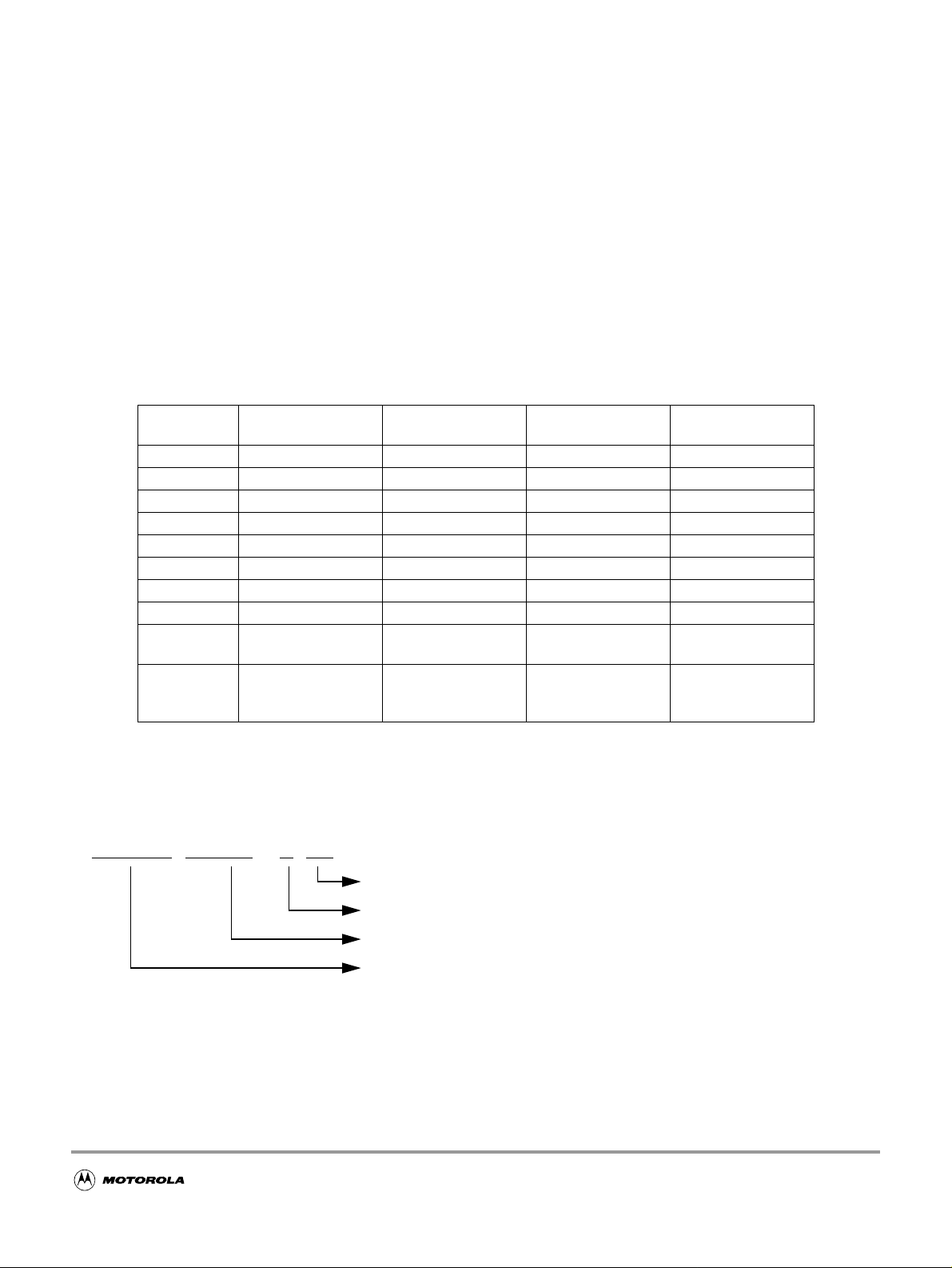
Derivative Differences
Table 0-1 shows the availability of peripheral modules on the various derivatives. For details about the
compatibility within the MC9S12D-Family refer also to engineering bulletin EB386.
Table 0-1 Derivative Differences
Generic
device
# of CANs 0322
CAN0 — ✓✓✓
CAN1 — ✓ ——
CAN4 — ✓✓✓
J1850/BDLC — — ✓ —
Package 112 LQFP/80 QFP 112 LQFP/80 QFP 112 LQFP/80 QFP 112 LQFP/80 QFP
Mask set L91N L91N L91N L91N
Temp Options C M, V, C M, V, C M, V, C
Package
Code
Notes
MC9S12A256 MC9S12DT256 MC9S12DJ256 MC9S12DG256
PV/FU PV/FU PV/FU PV/FU
An errata exists
contact Sales
Office
An errata exists
contact Sales
Office
An errata exists
contact Sales
Office
An errata exists
contact Sales
Office
The following figure provides an ordering number example for the MC9S12H-Family devices.
MC9S12 DT256 C FU
Package Option
Temperature Option
Temperature Options
C = -40˚C to 85˚C
V = -40˚C to 105˚C
M = -40˚C to 125˚C
Device Title
Package Options
Controller Family
FU = 80QFP
PV = 112 LQFP
Figure 0-1 Order Partnumber Example
15

MC9S12DT256 Device User Guide — V03.03
The following items should be considered when using a derivative (Table 0-1):
• Registers
– Do not write or read CAN0 registers (after reset: address range $0140 - $017F), if using a
derivative without CAN0.
– Do not write or read CAN1registers (after reset: address range $0180 - $01BF), if using a
derivative without CAN1.
– Do not write or read CAN4 registers (after reset: address range $0280 - $02BF), if using a
derivative without CAN4.
– Do not write or read BDLC registers (after reset: address range $00E8 - $00EF), if using a
derivative without BDLC.
• Interrupts
– Fill the four CAN0 interrupt vectors ($FFB0 - $FFB7) according to your coding policies for
unused interrupts, if using a derivative without CAN0.
– Fill the four CAN1 interrupt vectors ($FFA8 - $FFAF) according to your coding policies for
unused interrupts, if using a derivative without CAN1.
– Fill the four CAN4 interrupt vectors ($FF90 - $FF97) according to your coding policies for
unused interrupts, if using a derivative without CAN4.
– Fill the BDLC interrupt vector ($FFC2, $FFC3) according to your coding policies for unused
interrupts, if using a derivative without BDLC.
• Ports
– The CAN0 pin functionality (TXCAN0, RXCAN0) is not available on port PJ7, PJ6, PM5,
PM4, PM3, PM2, PM1 and PM0, if using a derivative without CAN0.
– The CAN1 pin functionality (TXCAN1, RXCAN1) is not available on port PM3 and PM2, if
using a derivative without CAN1.
– The CAN4 pin functionality (TXCAN4, RXCAN4) is not available on port PJ7, PJ6, PM5,
PM7, PM6, PM5 and PM4, if using a derivative without CAN0.
– The BDLC pin functionality (TXB, RXB) is not available on port PM1 and PM0, if using a
derivative without BDLC.
– Do not write MODRR1 and MODRR0 bits of Module Routing Register (PIM_9DP256 Block
Guide), if using a derivative without CAN0.
– Do not write MODRR3 and MODRR2 bits of Module Routing Register (PIM_9DP256 Block
Guide), if using a derivative without CAN4.
Document References
16
MC9S12DT256 Device User Guide — V03.03
The Device Guide provides information about the MC9S12DT256 device made up of standard HCS12
blocks and the HCS12 processor core.
This document is part of the customer documentation. A complete set of device manuals also includes the
HCS12 Core User Guide and all the individual Block Guides of the implemented modules. In a effort to
reduce redundancy all module specific information is located only in the respective Block Guide. If
applicable, special implementation details of the module are given in the block description sections of this
document.
See Table 0-2 for names and versions of the referenced documents throughout the Device User Guide.
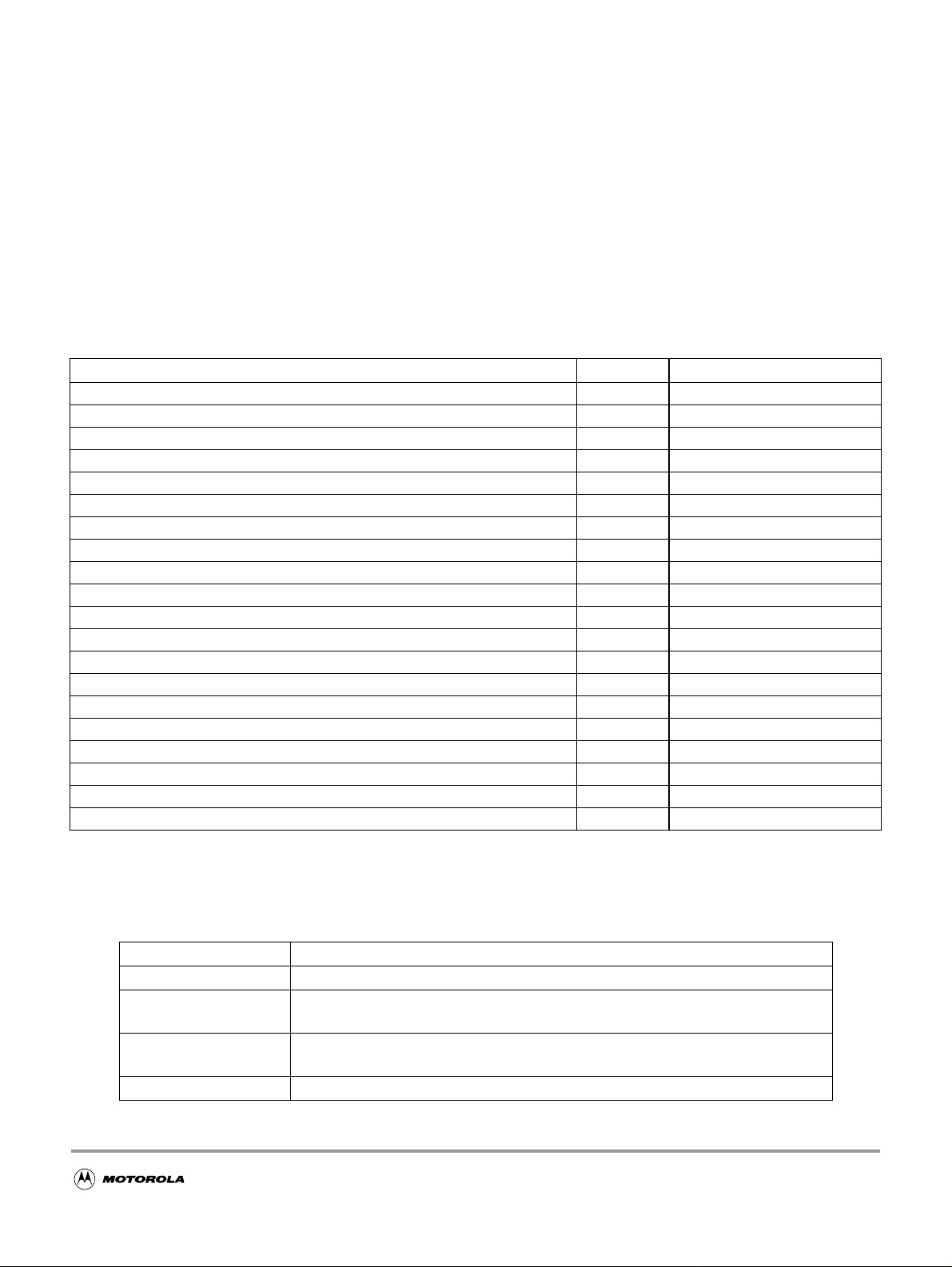
Table 0-2 Document References
User Guide Version Document Order Number
CPU12 Reference Manual V04 CPU12RM/AD
HCS12 Multiplexed External Bus Interface (MEBI) Block Guide V03 S12MEBIV3/D
HCS12 Module Mapping Control (MMC) Block Guide V04 S12MMCV4/D
HCS12 Interrupt (INT) Block Guide V01 S12INTV1/D
HCS12 Background Debug (BDM) Block Guide V04 S12BDMV4/D
HCS12 Breakpoint (BKP) Block Guide V01 S12BKPV1/D
Clock and Reset Generator (CRG) Block User Guide V04 S12CRGV4/D
Enhanced Capture Timer (ECT_16B8C) Block User Guide V01 S12ECT16B8CV1/D
Analog to Digital Converter 10 Bit 8 Channels (ATD_10B8C) Block User Guide V02 S12ATD10B8CV2/D
Inter IC Bus (IIC) Block User Guide V02 S12IICV2/D
Asynchronous Serial Interface (SCI) Block User Guide V02 S12SCIV2/D
Serial Peripheral Interface (SPI) Block User Guide V03 S12SPIV3/D
Pulse Width Modulator 8 Bit 8 Channel (PWM_8B8C) Block User Guide V01 S12PWM8B8CV1/D
256 K Byte Flash (FTS256K) Block User Guide V03 S12FTS256KV3/D
4K Byte EEPROM (EETS4K) Block User Guide V02 S12EETS4KV2/D
Byte Level Data Link Controller -J1850 (BDLC) Block User Guide V01 S12BDLCV1/D
Motorola Scalable CAN (MSCAN) Block User Guide V02 S12MSCANV2/D
Voltage Regulator (VREG) Block User Guide V01 S12VREGV1/D
Port Integration Module (PIM_9DP256) Block User Guide V03 S12PIM9DP256V3/D
Oscillator (OSC) Block Guide V02 S12OSCV2/D
Table 0-3 shows the Specification Change Summary for Maskset L91N.
Table 0-3 Specification Change Summary for Maskset L91N
Block Spec Change
MCU_9DT256 removed CAN2 and CAN3
HCS12 V1.5
HCS12 V1.5
CRG Maskset includes an additional Pierce Oscillator
The Background Debug Module includes an Acknowledge Protocol (two
additional hardware commands ACK_ENABLE/ACK_DISABLE)
The state of PK7/ROMCTL is latched into ROMON Bit during RESET into
Emulation Mode or Normal Expanded Mode
17

MC9S12DT256 Device User Guide — V03.03
Table 0-3 Specification Change Summary for Maskset L91N
Block Spec Change
EETS4K/FTS256K Reliability Specification for Non Volatile Memories
PIM_9DP256 CAN0 can be routed to PORTJ
18

User Guide End Sheet
MC9S12DT256 Device User Guide — V03.03
129

MC9S12DT256 Device User Guide — V03.03
130
FINAL PAGE OF
130
PAGES

MC9S12DT256 Device User Guide — V03.03
Section 1 IntroductionMC9S12DT256
1.1 Overview
The MC9S12DT256 microcontroller unit (MCU) is a 16-bit device composed of standard on-chip
peripherals including a 16-bit central processing unit (HCS12 CPU), 256K bytes of Flash EEPROM, 12K
bytes of RAM, 4K bytes of EEPROM, two asynchronous serial communications interfaces (SCI), three
serial peripheral interfaces (SPI), an 8-channel IC/OC enhanced capture timer, two 8-channel, 10-bit
analog-to-digital converters(ADC),an 8-channel pulse-width modulator(PWM),a digital Byte Data Link
Controller (BDLC), 29 discrete digital I/O channels (Port A, Port B, Port K and Port E), 20 discrete digital
I/O lines with interrupt and wakeup capability, three CAN 2.0 A, B software compatible modules
(MSCAN12), and an Inter-IC Bus. The MC9S12DT256 has full 16-bit data paths throughout. However,
the external bus can operate in an 8-bit narrow mode so single 8-bit wide memory can be interfaced for
lower cost systems. The inclusion of a PLL circuit allows power consumption and performance to be
adjusted to suit operational requirements.
1.2 Features
• HCS12 Core
– 16-bit HCS12 CPU
i. Upward compatible with M68HC11 instruction set
ii. Interrupt stacking and programmer’s model identical to M68HC11
iii.Instruction queue
iv.Enhanced indexed addressing
– MEBI (Multiplexed External Bus Interface)
– MMC (Module Mapping Control)
– INT (Interrupt control)
– BKP (Breakpoints)
– BDM (Background Debug Mode)
• CRG
– Low current Colpitts or Pierce oscillator
– PLL
– COP watchdog
– Real time interrupt
– Clock Monitor
• 8-bit and 4-bit ports with interrupt functionality
– Digital filtering
19

MC9S12DT256 Device User Guide — V03.03
– Programmable rising or falling edge trigger
• Memory
– 256K Flash EEPROM
– 4K byte EEPROM
– 12K byte RAM
• Two 8-channel Analog-to-Digital Converters
– 10-bit resolution
– External conversion trigger capability
• Three 1M bit per second, CAN 2.0 A, B software compatible modules
– Five receive and three transmit buffers
– Flexible identifier filter programmable as 2 x 32 bit, 4 x 16 bit or 8 x 8 bit
– Four separate interrupt channels for Rx, Tx, error and wake-up
– Low-pass filter wake-up function
– Loop-back for self test operation
• Enhanced Capture Timer
– 16-bit main counter with 7-bit prescaler
– 8 programmable input capture or output compare channels
– Four 8-bit or two 16-bit pulse accumulators
• 8 PWM channels
– Programmable period and duty cycle
– 8-bit 8-channel or 16-bit 4-channel
– Separate control for each pulse width and duty cycle
– Center-aligned or left-aligned outputs
– Programmable clock select logic with a wide range of frequencies
– Fast emergency shutdown input
– Usable as interrupt inputs
• Serial interfaces
– Two asynchronous Serial Communications Interfaces (SCI)
– Three Synchronous Serial Peripheral Interface (SPI)
• Byte Data Link Controller (BDLC)
– SAE J1850 Class B Data Communications Network Interface Compatible and ISO Compatible
for Low-Speed (<125 Kbps) Serial Data Communications in Automotive Applications
• Inter-IC Bus (IIC)
20

– Compatible with I2C Bus standard
– Multi-master operation
– Software programmable for one of 256 different serial clock frequencies
• 112-Pin LQFP package
– I/O lines with 5V input and drive capability
– 5V A/D converter inputs
– Operation at 50MHz equivalent to 25MHz Bus Speed
– Development support
– Single-wire background debug™ mode (BDM)
– On-chip hardware breakpoints
1.3 Modes of Operation
User modes
MC9S12DT256 Device User Guide — V03.03
• Normal and Emulation Operating Modes
– Normal Single-Chip Mode
– Normal Expanded Wide Mode
– Normal Expanded Narrow Mode
– Emulation Expanded Wide Mode
– Emulation Expanded Narrow Mode
• Special Operating Modes
– Special Single-Chip Mode with active Background Debug Mode
– Special Test Mode (Motorola use only)
– Special Peripheral Mode (Motorola use only)
Low power modes
• Stop Mode
• Pseudo Stop Mode
• Wait Mode
21

MC9S12DT256 Device User Guide — V03.03
1.4 Block Diagram
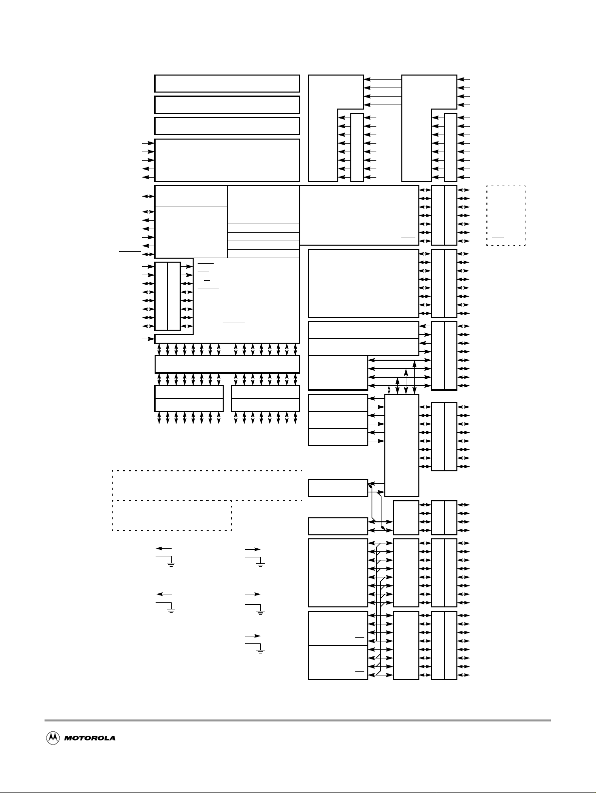
Figure 1-1 shows a block diagram of the MC9S12DT256 device.
22
MC9S12DT256 Device User Guide — V03.03
Figure 1-1 MC9S12DT256 Block Diagram
VDDR
VSSR
VREGEN
VDD1,2
VSS1,2
BKGD
XFC
VDDPLL
VSSPLL
EXTAL
XTAL
RESET
PE0
PE1
PE2
PE3
PE4
PE5
PE6
PE7
TEST
Multiplexed
Wide Bus
Multiplexed
Narrow Bus
Internal Logic 2.5V
VDD1,2
VSS1,2
PLL 2.5V
VDDPLL
VSSPLL
256K Byte Flash EEPROM
12K Byte RAM
4K Byte EEPROM
Voltage Regulator
Single-wire Background
Debug Module
Clock and
Reset
PLL
Generation
Module
XIRQ
IRQ
W
R/
LSTRB
DDRE
ECLK
MODA
MODB
NOACC/
XCLKS
PTE
Multiplexed Address/Data Bus
DDRA DDRB
PTA PTB
PA4
PA3
PA2
PA1
ADDR11
ADDR10
ADDR9
DATA11
DATA10
DATA9
DATA3
DATA2
DATA1
PA0
ADDR8
DATA8
DATA0
PA7
PA6
PA5
ADDR15
ADDR14
ADDR13
DATA15
DATA14
DATA13
DATA7
DATA6
DATA5
ADDR12
DATA12
DATA4
I/O Driver 5V
VDDX
VSSX
A/D Converter 5V &
Voltage Regulator Reference
VDDA
VSSA
Voltage Regulator 5V & I/O
VDDR
VSSR
CPU12
Periodic Interrupt
COP Watchdog
Clock Monitor
Breakpoints
System
Integration
Module
(SIM)
PB4
PB6
PB5
ADDR6
ADDR5
DATA6
DATA5
PB3
ADDR4
ADDR3
DATA4
DATA3
PB7
ADDR7
DATA7
PB2
PB1
ADDR2
ADDR1
DATA2
DATA1
ATD0
AN0
AN1
AN2
AN3
AN4
AN5
AN6
AN7
Enhanced Capture
Timer
SCI0
SCI1
SPI0
BDLC
(J1850)
CAN0
PB0
CAN1
ADDR0
CAN4
DATA0
IIC
PWM
SPI1
SPI2
VRH
VRL
VDDA
VSSA
PPAGE
MISO
MOSI
SCK
RXB
TXB
RXCAN
TXCAN
RXCAN
TXCAN
RXCAN
TXCAN
SDA
SCL
PWM0
PWM1
PWM2
PWM3
PWM4
PWM5
PWM6
PWM7
MISO
MOSI
SCK
MISO
MOSI
SCK
SS
SS
SS
AD0
ATD1
PAD00
PAD01
PAD02
PAD03
PAD04
PAD05
PAD06
PAD07
AN0
AN1
AN2
AN3
AN4
AN5
AN6
AN7
PIX0
PIX1
PIX2
PIX3
PIX4
PIX5
ECS
IOC0
IOC1
IOC2
IOC3
IOC4
IOC5
IOC6
IOC7
RXD
TXD
RXD
TXD
Module to Port Routing
KWJ0
KWJ1
KWJ6
KWJ7
KWP0
KWP1
KWP2
KWP3
KWP4
KWP5
KWP6
KWP7
KWH0
KWH1
KWH2
KWH3
KWH4
KWH5
KWH6
KWH7
VRH
VRL
VDDA
VSSA
DDRK
DDRT
DDRS
DDRM
DDRJ
DDRP
DDRH
AD1
PTK
PTT
PTS
PTM
PTJ
PTP
PTH
VRH
VRL
VDDA
VSSA
PAD08
PAD09
PAD10
PAD11
PAD12
PAD13
PAD14
PAD15
PK0
PK1
PK2
PK3
PK4
PK5
PK7
PT0
PT1
PT2
PT3
PT4
PT5
PT6
PT7
PS0
PS1
PS2
PS3
PS4
PS5
PS6
PS7
PM0
PM1
PM2
PM3
PM4
PM5
PM6
PM7
PJ0
PJ1
PJ6
PJ7
PP0
PP1
PP2
PP3
PP4
PP5
PP6
PP7
PH0
PH1
PH2
PH3
PH4
PH5
PH6
PH7
XADDR14
XADDR15
XADDR16
XADDR17
XADDR18
XADDR19
ECS
Signals shown in Bold are not available on the 80 Pin Package
23
MC9S12DT256 Device User Guide — V03.03
1.5 Device Memory Map
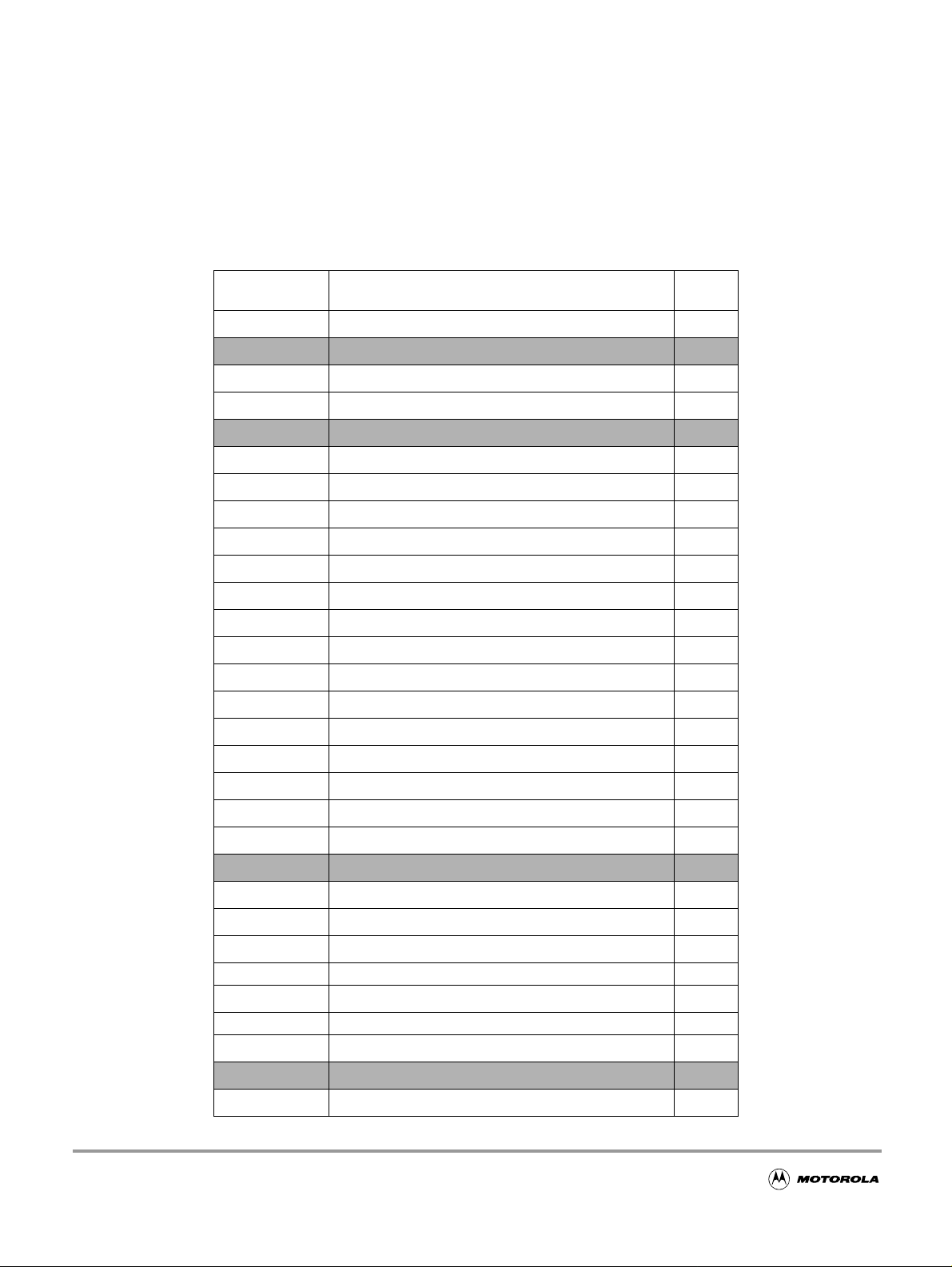
Table1-1andFigure 1-2 showthedevice memory mapofthe MC9S12DT256 afterreset. Note thatafter
reset the bottom 1k of the EEPROM ($0000 - $03FF) are hidden by the register space.
Table 1-1 Device Memory Map
Address Module
$0000 - $0017
$0018 - $0019
$001A - $001B
$001C - $001F
$0020 - $0027
$0028 - $002F
$0030 - $0033
$0034 - $003F
$0040 - $007F
$0080 - $009F
$00A0 - $00C7
$00C8 - $00CF
$00D0 - $00D7
$00D8 - $00DF
$00E0 - $00E7
$00E8 - $00EF
$00F0 - $00F7
$00F8 - $00FF
$0100- $010F
$0110 - $011B
$011C - $011F
$0120 - $013F
$0140 - $017F
$0180 - $01BF
$01C0 - $01FF Reserved 64
$0200 - $023F
$0240 - $027F Port Integration Module (PIM) 64
$0280 - $02BF
$02C0 - $03FF
$0000 - $0FFF
CORE (Ports A, B, E, Modes, Inits, Test)
Reserved
Device ID register (PARTID)
CORE (MEMSIZ, IRQ, HPRIO)
Reserved
CORE (Background Debug Mode)
CORE (PPAGE, Port K)
Clock and Reset Generator (PLL, RTI, COP)
Enhanced Capture Timer 16-bit 8 channels
Analog to Digital Converter 10-bit 8 channels (ATD0)
Pulse Width Modulator 8-bit 8 channels (PWM)
Serial Communications Interface (SCI0)
Serial Communications Interface (SCI1)
Serial Peripheral Interface (SPI0)
Inter IC Bus
Byte Data Link Controller (BDLC)
Serial Peripheral Interface (SPI1)
Serial Peripheral Interface (SPI2)
Flash Control Register
EEPROM Control Register
Reserved
Analog to Digital Converter 10-bit 8 channels (ATD1)
Motorola Scalable Can (CAN0)
Motorola Scalable Can (CAN1)
Reserved
Motorola Scalable Can (CAN4)
Reserved
EEPROM array
Size
(Bytes)
24
12
64
32
40
16
12
32
64
64
64
64
320
4096
2
2
4
8
8
4
8
8
8
8
8
8
8
4
24

MC9S12DT256 Device User Guide — V03.03
Table 1-1 Device Memory Map
Address Module
$1000 - $3FFF
$4000 - $7FFF
$8000 - $BFFF
$C000 - $FFFF
RAM array
Fixed Flash EEPROM array
incl. 0.5K, 1K, 2K or 4K Protected Sector at start
Flash EEPROM Page Window
Fixed Flash EEPROM array
incl. 0.5K, 1K, 2K or 4K Protected Sector at end
and 256 bytes of Vector Space at $FF80 - $FFFF
Size
(Bytes)
12288
16384
16384
16384
25
MC9S12DT256 Device User Guide — V03.03
Figure 1-2 MC9S12DT256 Memory Map
$0000
$0400
$1000
$4000
$8000
EXTERN
$0000
$03FF
$0000
$0FFF
$1000
$3FFF
$4000
$7FFF
$8000
REGISTERS
(Mappable to any 2k Block
within the first 32K)
4K Bytes EEPROM
(Mappable to any 4K Block)
12K Bytes RAM
(Mappable to any 16K
and alignable to top or
bottom)
16K Fixed Flash
Page $3E = 62
(This is dependant on the
state of the ROMHM bit)
16K Page Window
16 x 16K Flash EEPROM
pages
$C000
$FF00
$FFFF
VECTORS
EXPANDED*
* Assuming that a ‘0’ was driven onto port K bit 7 during MCU
is reset into normal expanded wide or narrow mode.
VECTORS
NORMAL
SINGLE CHIP
VECTORS
SPECIAL
SINGLE CHIP
$BFFF
$C000
16K Fixed Flash
Page $3F = 63
$FFFF
$FF00
BDM
(if active)
$FFFF
26
MC9S12DT256 Device User Guide — V03.03
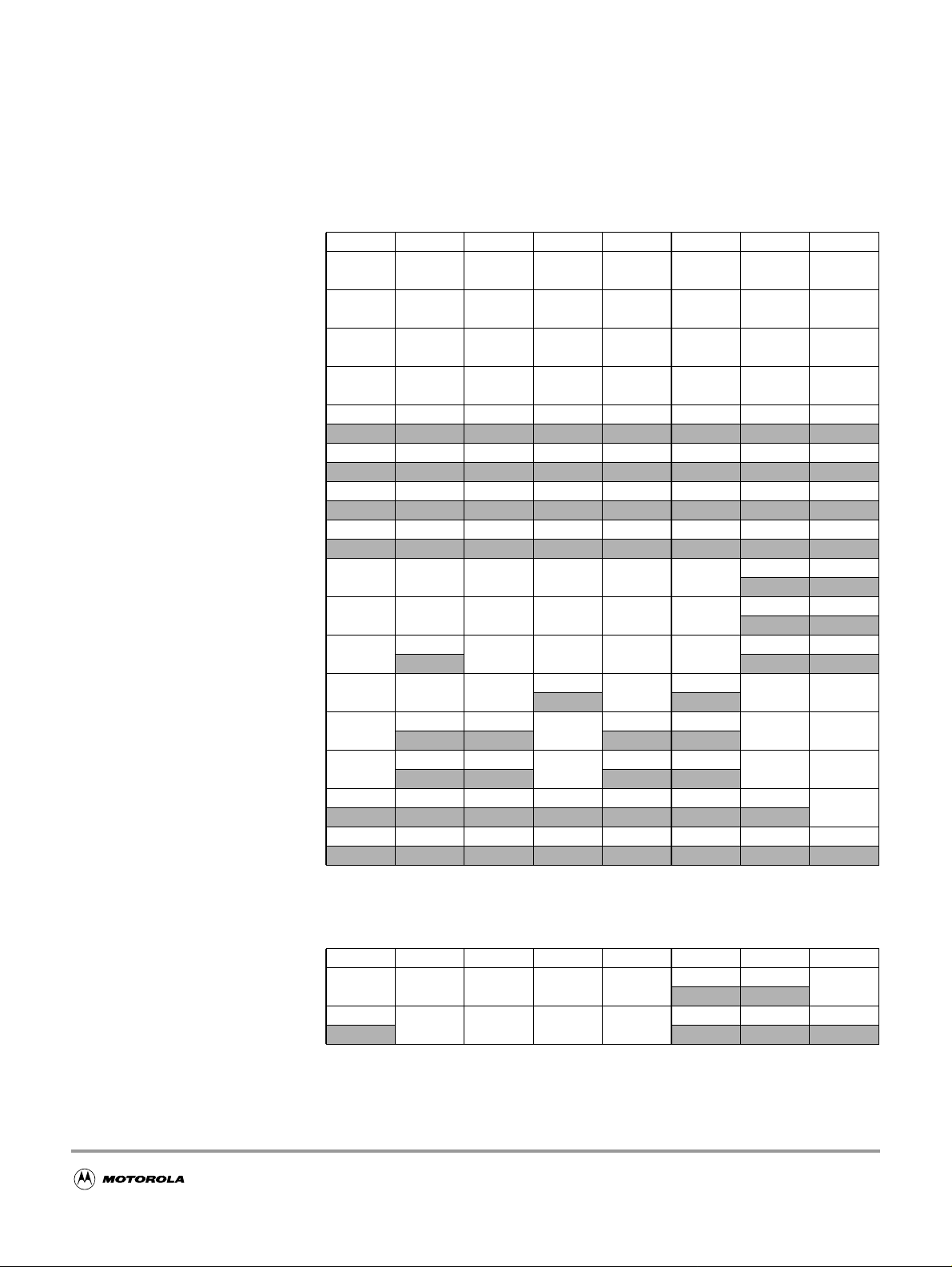
1.6 Detailed Register Map
The following tables show the detailed register map of the MC9S12DT256.
$0000 - $000F MEBI map 1 of 3 (Core User Guide)
Address Name Bit 7 Bit 6 Bit 5 Bit 4 Bit 3 Bit 2 Bit 1 Bit 0
$0000
$0001
$0002
$0003
$0004
$0005
$0006
$0007
$0008
$0009
$000A
$000B
$000C
$000D
$000E
$000F
PORTA
PORTB
DDRA
DDRB
Reserved
Reserved
Reserved
Reserved
PORTE
DDRE
PEAR
MODE
PUCR
RDRIV
EBICTL
Reserved
Read:
Write:
Read:
Write:
Read:
Write:
Read:
Write:
Read: 00000000
Write:
Read: 00000000
Write:
Read: 00000000
Write:
Read: 00000000
Write:
Read:
Write:
Read:
Write:
Read:
Write:
Read:
Write:
Read:
Write:
Read:
Write:
Read: 0000000
Write:
Read: 00000000
Write:
Bit 7 654321Bit 0
Bit 7 654321Bit 0
Bit 7 654321Bit 0
Bit 7 654321Bit 0
Bit 7 65432
Bit 7 6543Bit 2
NOACCE
MODC MODB MODA
PUPKE
RDPK
0
00
00
PIPOE NECLK LSTRE RDWE
PUPEE
RDPE
0
IVIS
00
00
0
PUPBE PUPAE
Bit 1 Bit 0
00
00
EMK EME
RDPB RDPA
ESTR
$0010 - $0014 MMC map 1 of 4 (Core User Guide)
Address Name Bit 7 Bit 6 Bit 5 Bit 4 Bit 3 Bit 2 Bit 1 Bit 0
$0010
$0011
INITRM
INITRG
Read:
Write:
Read: 0
Write:
RAM15 RAM14 RAM13 RAM12 RAM11
REG14 REG13 REG12 REG11
00
000
RAMHAL
27
MC9S12DT256 Device User Guide — V03.03
$0010 - $0014 MMC map 1 of 4 (Core User Guide)
Address Name Bit 7 Bit 6 Bit 5 Bit 4 Bit 3 Bit 2 Bit 1 Bit 0
$0012
$0013
$0014 Reserved
INITEE
MISC
Read:
Write:
Read: 0000
Write:
Read: 00000000
Write:
EE15 EE14 EE13 EE12 EE11
EXSTR1 EXSTR0 ROMHM ROMON
00
$0015 - $0016 INT map 1 of 2 (Core User Guide)
Address Name Bit 7 Bit 6 Bit 5 Bit 4 Bit 3 Bit 2 Bit 1 Bit 0
$0015
$0016
ITCR
ITEST
Read: 0 0 0
Write:
Read:
Write:
INTE INTC INTA INT8 INT6 INT4 INT2 INT0
WRINT ADR3 ADR2 ADR1 ADR0
$0017 - $0017 MMC map 2 of 4 (Core User Guide)
EEON
Address Name Bit 7 Bit 6 Bit 5 Bit 4 Bit 3 Bit 2 Bit 1 Bit 0
$0017 Reserved
Read: 00000000
Write:
$0018 - $001B Miscellaneous Peripherals (Device User Guide,Table 1-3)
Address Name Bit 7 Bit 6 Bit 5 Bit 4 Bit 3 Bit 2 Bit 1 Bit 0
$0018
$0019
$001A
$001B
Reserved
Reserved
PARTIDH
PARTIDL
Read: 00000000
Write:
Read: 00000000
Write:
Read: ID15 ID14 ID13 ID12 ID11 ID10 ID9 ID8
Write:
Read: ID7 ID6 ID5 ID4 ID3 ID2 ID1 ID0
Write:
$001C - $001D MMC map 3 of 4 (Core and Device User Guide,Table 1-4)
Address Name Bit 7 Bit 6 Bit 5 Bit 4 Bit 3 Bit 2 Bit 1 Bit 0
$001C
$001D
MEMSIZ0
MEMSIZ1
Read: reg_sw0 0 eep_sw1 eep_sw0 0 ram_sw2 ram_sw1 ram_sw0
Write:
Read: rom_sw1 rom_sw0 0000pag_sw1 pag_sw0
Write:
28
 Loading...