

Motorola MC9S12DJ128EVPV, MC9S12DJ128EMPV, MC9S12DJ128ECPV, MC9S12DJ128CFU, MC9S12DJ128CPV Datasheet
...
Motorola reserves the right to make changes without further notice to any products herein to improve reliability, function or
design. Motorola does not assume any liability arising out of the application or use of any product or circuit described herein;
neither does it convey any license under its patent rights nor the rights of others. Motorola products are not designed, intended,
or authorized for use as components in systems intended for surgical implant into the body, or other applications intended to
support or sustain life, or for any other application in which the failure of the Motorola product could create a situation where
personal injury or death may occur. Should Buyer purchase or use Motorola products for any such unintended or unauthorized
application,Buyershallindemnify andhold Motorolaand itsofficers, employees,subsidiaries, affiliates,and distributorsharmless
against all claims, costs, damages, and expenses, and reasonable attorney fees arising out of, directly or indirectly, any claim of
personal injury or death associated with such unintended or unauthorized use, even if such claim alleges that Motorola was
negligent regarding the design or manufacture of the part.
DOCUMENT NUMBER
9S12DT128DGV2/D
1
MC9S12DT128
Device User Guide
V02.09
Covers also
MC9S12DT128E, MC9S12DG128E,
MC9S12DJ128E, MC9S12DG128,
MC9S12DJ128, MC9S12DB128
Original Release Date: 18 June 2001
Revised: 15 October 2003
Motorola, Inc

MC9S12DT128 Device User Guide — V02.09
2
Revision History
Version
Number
Revision
Date
Effective
Date
Author Description of Changes
V01.00
18 Jun
2001
18 June
2001
Initial version (parent doc v2.03 dug for dp256).
V01.01
23 July
2001
23 July
2001
Updated version after review
V01.02
23 Sep
2001
23 Sep
2001
Changed Partname, added pierce mode, updated electrical
characteristics
some minor corrections
V01.03
12 Oct
2001
12 Oct
2001
Replaced Star12 by HCS12
V01.04
27 Feb
2002
27 Feb
2002
Updated electrical spec after MC-Qualification (IOL/IOH), Data for
Pierce, NVM reliability
New document numbering. Corrected Typos
V01.05
4 Mar
2002
4 Mar
2002
Increased VDD to 2.35V, removed min. oscillator startup
Removed Document order number except from Cover Sheet
V01.06
8 July
2002
22 July
2002
Added:
Pull-up columns to signal table,
example for PLL Filter calculation,
Thermal values for junction to board and package,
BGND pin pull-up
Part Order Information
Global Register Table
Chip Configuration Summary
Modified:
Reduced Wait and Run IDD values
Mode of Operation chapter
changed leakage current for ADC inputs down to +-1uA
Corrected:
Interrupt vector table enable register inconsistencies
PCB layout for 80QFP VREGEN position
V02.00
11 Jan
2002
11 Jan
2002
NEW MASKSET
Changed part number from DTB128 to DT128
Functional Changes:
ROMCTL changes in Emulation Mode
80 Pin Byteflight package Option available
Flash with 2 Bit Backdoor Key Enable
Additional CAN0 routing to PJ7,6
Improved BDM with sync and acknowledge capabilities
New Part ID number
Improvements:
Significantly improved NVM reliability data
Corrections:
Interrupt vector Table
V02.01
01 Feb
2002
01 Feb
2002
Updated Block User Guide versions in preface
Updated Appendix A Electrical Characteristics

MC9S12DT128 Device User Guide — V02.09
3
V02.02
08 Mar
2002
08 Mar
2002
Changed XCLKS to PE7 in Table 2-2
Updated device part numbers in Figure 2-1
Updated BDM clock in Figure 3-1
Removed SIM descriptionin overview & n
UPOSC
spec in Table A-15
Updated electrical spec of VDD & VDDPLL (Table A-4), IOL/IOH
(Table A-6), C
INS
(Table A-9), CIN(Table A-6 & A-15),
Updated interrupt pulse timing variables in Table A-6
Updated device part numbers in Figure 2-1
Added document numbers on cover page and Table 0-2
V02.03
14 Mar
2002
14 Mar
2002
Cleaned up Fig. 1-1, 2-1
Updated Section 1.5 descriptions
Corrected PE assignment in Table 2-2, Fig. 2-5,6,7.
Corrected NVM sizes in Sections 16, 17
Added I
REF
spec for 1ATD in Table A-8
Added Blank Check in A.3.1.5 and Table A-11
Updated CRG spec in Table A-15
V02.04
16 Aug
2002
16 Aug
2002
Added:
Pull-up columns to signal table,
Example for PLL Filter calculation,
Thermal values for junction to board and package,
BGND pin pull-up
Part Order Information
Global Register Table
Chip Configuration Summary
Device specific info on CRG
Modified:
Reduced Wait and Run IDD values
Mode of Operation chapter
Changed leakage current for ADC inputs down to +-1uA
Minor modification of PLL frequency/ voltage gain values
Corrected:
Pin names/functions on 80 pin packages
Interrupt vector table enable register inconsistencies
PCB layout for 80QFP VREGEN position
V02.05
12 Sep
2002
12 Sep
2002
Corrected:
Register address mismatches in 1.5.1
V02.06
06 Nov
2002
06 Nov
2002
Removed document order no. from Revision History pages
Renamed "Preface" section to "Derivative Differences and
Document references". Added details for derivatives missing
CAN0/1/4, BDLC, IIC and/or Byteflight
Added 2L40K mask set in section 1.6
Added OSC User Guide in Preface, “Document References”
Added oscillator clock connection to BDM in S12_CORE in fig 3-1
Corrected several register and bit names in “Local Enable” column
of Table 5.1 Interrupt Vector Locations
Section HCS12 Core Block Description: mentioned alternate clock
of BDM to be equivalent to oscillator clock
Added new section: “Oscillator (OSC) Block Description”
Corrected in footnote of Table "PLL Characteristics": fOSC = 4MHz
Version
Number
Revision
Date
Effective
Date
Author Description of Changes

MC9S12DT128 Device User Guide — V02.09
4
V02.07
29 Jan
2003
29 Jan
2003
Added 3L40K mask set in section 1.6
Corrected register entries in section 1.5.1 “Detailed Memory Map”
Updated description for ROMCTL in section 2.3.31
Updated section 4.3.3 “Unsecuring the Microcontroller”
Corrected and updated device-specific information for OSC
(section 8.1) & Byteflight (section 15.1)
Updated footnote in Table A-4 “Operating Conditions”
Changed reference of VDDM to VDDR in section A.1.8
Removed footnote on input leakage current in Table A-6 “5V I/O
Characteristics”
V02.08
26 Feb
2003
26 Feb
2003
Added part numbers MC9S12DT128E, MC9S12DG128E, and
MC9S12DJ128E in “Preface” and related part number references
Removed mask sets 0L40K and 2L40K from Table 1-3
V02.09
15 Oct
2003
15 Oct
2003
Replaced references to HCS12 Core Guide by the individual
HCS12 Block guides in Table 0-2, section 1.5.1, and section 6;
updated Fig.3-1 “ClockConnections” to show the individual HCS12
blocks
Corrected PIM module name and document order number in Table
0-2 “Document References”
Corrected ECT pulse accumulators description in section 1.2
“Features”
Corrected KWP5 pin name in Fig 2-1 112LQFP pin assignments
Corrected pull resistor CTRL/reset states for PE7 and PE4-PE0 in
Table 2.1 “Signal Properties”
Mentioned “S12LRAE” bootloader in Flash section 17
Corrected footnote on clamp of TEST pin under Table A-1
“Absolute Maximum Ratings”
Corrected minimum bus frequency to 0.25MHz in Table A-4
“Operating Conditions”
Replaced “burst programming” by “row programming” in A.3 “NVM,
Flash and EEPROM”
Corrected blank check time for EEPROM in Table A-11 “NVM
Timing Characteristics”
Corrected operating frequency in Table A-18 “SPI Master/Slave
Mode Timing Characteristics
Version
Number
Revision
Date
Effective
Date
Author Description of Changes

MC9S12DT128 Device User Guide — V02.09
5

MC9S12DT128 Device User Guide — V02.09
6

MC9S12DT128 Device User Guide — V02.09
7
Table of Contents
Section 1 Introduction. . . . . . . . . . . . . . . . . . . . . . . . . . . . . . . . . . . . . . . . . . . .25
1.1 Overview. . . . . . . . . . . . . . . . . . . . . . . . . . . . . . . . . . . . . . . . . . . . . . . . . . . . . . . . . . . . .25
1.2 Features . . . . . . . . . . . . . . . . . . . . . . . . . . . . . . . . . . . . . . . . . . . . . . . . . . . . . . . . . . . . .25
1.3 Modes of Operation . . . . . . . . . . . . . . . . . . . . . . . . . . . . . . . . . . . . . . . . . . . . . . . . . . . .27
1.4 Block Diagram . . . . . . . . . . . . . . . . . . . . . . . . . . . . . . . . . . . . . . . . . . . . . . . . . . . . . . . .28
1.5 Device Memory Map. . . . . . . . . . . . . . . . . . . . . . . . . . . . . . . . . . . . . . . . . . . . . . . . . . . .30
1.5.1 Detailed Register Map . . . . . . . . . . . . . . . . . . . . . . . . . . . . . . . . . . . . . . . . . . . . . . . .32
1.6 Part ID Assignments. . . . . . . . . . . . . . . . . . . . . . . . . . . . . . . . . . . . . . . . . . . . . . . . . . . .55
Section 2 Signal Description . . . . . . . . . . . . . . . . . . . . . . . . . . . . . . . . . . . . . .57
2.1 Device Pinout . . . . . . . . . . . . . . . . . . . . . . . . . . . . . . . . . . . . . . . . . . . . . . . . . . . . . . . . .57
2.2 Signal Properties Summary . . . . . . . . . . . . . . . . . . . . . . . . . . . . . . . . . . . . . . . . . . . . . .60
2.3 Detailed Signal Descriptions. . . . . . . . . . . . . . . . . . . . . . . . . . . . . . . . . . . . . . . . . . . . . .64
2.3.1 EXTAL, XTAL — Oscillator Pins . . . . . . . . . . . . . . . . . . . . . . . . . . . . . . . . . . . . . . . .64
2.3.2 RESET — External Reset Pin . . . . . . . . . . . . . . . . . . . . . . . . . . . . . . . . . . . . . . . . . .64
2.3.3 TEST — Test Pin. . . . . . . . . . . . . . . . . . . . . . . . . . . . . . . . . . . . . . . . . . . . . . . . . . . .64
2.3.4 XFC — PLL Loop Filter Pin . . . . . . . . . . . . . . . . . . . . . . . . . . . . . . . . . . . . . . . . . . . .64
2.3.5 BKGD / TAGHI / MODC — Background Debug, Tag High, and Mode Pin . . . . . . . .64
2.3.6 PAD[15] / AN1[7] / ETRIG1 — Port AD Input Pin [15] . . . . . . . . . . . . . . . . . . . . . . . .65
2.3.7 PAD[14:8] / AN1[6:0] — Port AD Input Pins [14:8]. . . . . . . . . . . . . . . . . . . . . . . . . . .65
2.3.8 PAD[7] / AN0[7] / ETRIG0 — Port AD Input Pin [7] . . . . . . . . . . . . . . . . . . . . . . . . . .65
2.3.9 PAD[6:0] / AN0[6:0] — Port AD Input Pins [6:0]. . . . . . . . . . . . . . . . . . . . . . . . . . . . .65
2.3.10 PA[7:0] / ADDR[15:8] / DATA[15:8] — Port A I/O Pins . . . . . . . . . . . . . . . . . . . . . . .65
2.3.11 PB[7:0] / ADDR[7:0] / DATA[7:0] — Port B I/O Pins . . . . . . . . . . . . . . . . . . . . . . . . .65
2.3.12 PE7 / NOACC / XCLKS — Port E I/O Pin 7. . . . . . . . . . . . . . . . . . . . . . . . . . . . . . . .65
2.3.13 PE6 / MODB / IPIPE1 — Port E I/O Pin 6 . . . . . . . . . . . . . . . . . . . . . . . . . . . . . . . . .67
2.3.14 PE5 / MODA / IPIPE0 — Port E I/O Pin 5 . . . . . . . . . . . . . . . . . . . . . . . . . . . . . . . . .67
2.3.15 PE4 / ECLK — Port E I/O Pin 4 . . . . . . . . . . . . . . . . . . . . . . . . . . . . . . . . . . . . . . . . .67
2.3.16 PE3 / LSTRB / TAGLO — Port E I/O Pin 3 . . . . . . . . . . . . . . . . . . . . . . . . . . . . . . . .67
2.3.17 PE2 / R/W — Port E I/O Pin 2 . . . . . . . . . . . . . . . . . . . . . . . . . . . . . . . . . . . . . . . . . .67
2.3.18 PE1 / IRQ — Port E Input Pin 1. . . . . . . . . . . . . . . . . . . . . . . . . . . . . . . . . . . . . . . . .67
2.3.19 PE0 / XIRQ — Port E Input Pin 0. . . . . . . . . . . . . . . . . . . . . . . . . . . . . . . . . . . . . . . .67
2.3.20 PH7 / KWH7 — Port H I/O Pin 7 . . . . . . . . . . . . . . . . . . . . . . . . . . . . . . . . . . . . . . . .67

MC9S12DT128 Device User Guide — V02.09
8
2.3.21 PH6 / KWH6 — Port H I/O Pin 6 . . . . . . . . . . . . . . . . . . . . . . . . . . . . . . . . . . . . . . . .68
2.3.22 PH5 / KWH5 — Port H I/O Pin 5 . . . . . . . . . . . . . . . . . . . . . . . . . . . . . . . . . . . . . . . .68
2.3.23 PH4 / KWH4 — Port H I/O Pin 2 . . . . . . . . . . . . . . . . . . . . . . . . . . . . . . . . . . . . . . . .68
2.3.24 PH3 / KWH3 / SS1 — Port H I/O Pin 3 . . . . . . . . . . . . . . . . . . . . . . . . . . . . . . . . . . .68
2.3.25 PH2 / KWH2 / SCK1 — Port H I/O Pin 2 . . . . . . . . . . . . . . . . . . . . . . . . . . . . . . . . . .68
2.3.26 PH1 / KWH1 / MOSI1 — Port H I/O Pin 1 . . . . . . . . . . . . . . . . . . . . . . . . . . . . . . . . .68
2.3.27 PH0 / KWH0 / MISO1 — Port H I/O Pin 0 . . . . . . . . . . . . . . . . . . . . . . . . . . . . . . . . .68
2.3.28 PJ7 / KWJ7 / TXCAN4 / SCL / TXCAN0 — PORT J I/O Pin 7. . . . . . . . . . . . . . . . . .68
2.3.29 PJ6 / KWJ6 / RXCAN4 / SDA / RXCAN0 — PORT J I/O Pin 6 . . . . . . . . . . . . . . . . .69
2.3.30 PJ[1:0] / KWJ[1:0] — Port J I/O Pins [1:0] . . . . . . . . . . . . . . . . . . . . . . . . . . . . . . . . .69
2.3.31 PK7 / ECS / ROMCTL — Port K I/O Pin 7. . . . . . . . . . . . . . . . . . . . . . . . . . . . . . . . .69
2.3.32 PK[5:0] / XADDR[19:14] — Port K I/O Pins [5:0] . . . . . . . . . . . . . . . . . . . . . . . . . . . .69
2.3.33 PM7 / BF_PSLM / TXCAN4 — Port M I/O Pin 7 . . . . . . . . . . . . . . . . . . . . . . . . . . . .69
2.3.34 PM6 / BF_PERR / RXCAN4 — Port M I/O Pin 6 . . . . . . . . . . . . . . . . . . . . . . . . . . . .69
2.3.35 PM5 / BF_PROK / TXCAN0 / TXCAN4 / SCK0 — Port M I/O Pin 5 . . . . . . . . . . . . .69
2.3.36 PM4 / BF_PSYN / RXCAN0 / RXCAN4/ MOSI0 — Port M I/O Pin 4. . . . . . . . . . . . .70
2.3.37 PM3 / TX_BF / TXCAN1 / TXCAN0 / SS0 — Port M I/O Pin 3 . . . . . . . . . . . . . . . . .70
2.3.38 PM2 / RX_BF / RXCAN1 / RXCAN0 / MISO0 — Port M I/O Pin 2. . . . . . . . . . . . . . .70
2.3.39 PM1 / TXCAN0 / TXB — Port M I/O Pin 1 . . . . . . . . . . . . . . . . . . . . . . . . . . . . . . . . .70
2.3.40 PM0 / RXCAN0 / RXB — Port M I/O Pin 0. . . . . . . . . . . . . . . . . . . . . . . . . . . . . . . . .70
2.3.41 PP7 / KWP7 / PWM7 — Port P I/O Pin 7. . . . . . . . . . . . . . . . . . . . . . . . . . . . . . . . . .70
2.3.42 PP6 / KWP6 / PWM6 — Port P I/O Pin 6. . . . . . . . . . . . . . . . . . . . . . . . . . . . . . . . . .70
2.3.43 PP5 / KWP5 / PWM5 — Port P I/O Pin 5. . . . . . . . . . . . . . . . . . . . . . . . . . . . . . . . . .71
2.3.44 PP4 / KWP4 / PWM4 — Port P I/O Pin 4. . . . . . . . . . . . . . . . . . . . . . . . . . . . . . . . . .71
2.3.45 PP3 / KWP3 / PWM3 / SS1 — Port P I/O Pin 3. . . . . . . . . . . . . . . . . . . . . . . . . . . . .71
2.3.46 PP2 / KWP2 / PWM2 / SCK1 — Port P I/O Pin 2 . . . . . . . . . . . . . . . . . . . . . . . . . . .71
2.3.47 PP1 / KWP1 / PWM1 / MOSI1 — Port P I/O Pin 1. . . . . . . . . . . . . . . . . . . . . . . . . . .71
2.3.48 PP0 / KWP0 / PWM0 / MISO1 — Port P I/O Pin 0. . . . . . . . . . . . . . . . . . . . . . . . . . .71
2.3.49 PS7 / SS0 — Port S I/O Pin 7 . . . . . . . . . . . . . . . . . . . . . . . . . . . . . . . . . . . . . . . . . .71
2.3.50 PS6 / SCK0 — Port S I/O Pin 6 . . . . . . . . . . . . . . . . . . . . . . . . . . . . . . . . . . . . . . . . .71
2.3.51 PS5 / MOSI0 — Port S I/O Pin 5 . . . . . . . . . . . . . . . . . . . . . . . . . . . . . . . . . . . . . . . .72
2.3.52 PS4 / MISO0 — Port S I/O Pin 4 . . . . . . . . . . . . . . . . . . . . . . . . . . . . . . . . . . . . . . . .72
2.3.53 PS3 / TXD1 — Port S I/O Pin 3 . . . . . . . . . . . . . . . . . . . . . . . . . . . . . . . . . . . . . . . . .72
2.3.54 PS2 / RXD1 — Port S I/O Pin 2. . . . . . . . . . . . . . . . . . . . . . . . . . . . . . . . . . . . . . . . .72
2.3.55 PS1 / TXD0 — Port S I/O Pin 1 . . . . . . . . . . . . . . . . . . . . . . . . . . . . . . . . . . . . . . . . .72
2.3.56 PS0 / RXD0 — Port S I/O Pin 0. . . . . . . . . . . . . . . . . . . . . . . . . . . . . . . . . . . . . . . . .72

MC9S12DT128 Device User Guide — V02.09
9
2.3.57 PT[7:0] / IOC[7:0] — Port T I/O Pins [7:0] . . . . . . . . . . . . . . . . . . . . . . . . . . . . . . . . .72
2.4 Power Supply Pins . . . . . . . . . . . . . . . . . . . . . . . . . . . . . . . . . . . . . . . . . . . . . . . . . . . . .72
2.4.1 VDDX,VSSX — Power & Ground Pins for I/O Drivers. . . . . . . . . . . . . . . . . . . . . . . .73
2.4.2 VDDR, VSSR — Power & Ground Pins for I/O Drivers & for Internal Voltage Regulator
73
2.4.3 VDD1, VDD2, VSS1, VSS2 — Internal Logic Power Supply Pins. . . . . . . . . . . . . . .73
2.4.4 VDDA, VSSA — Power Supply Pins for ATD and VREG . . . . . . . . . . . . . . . . . . . . .74
2.4.5 VRH, VRL — ATD Reference Voltage Input Pins . . . . . . . . . . . . . . . . . . . . . . . . . . .74
2.4.6 VDDPLL, VSSPLL — Power Supply Pins for PLL. . . . . . . . . . . . . . . . . . . . . . . . . . .74
2.4.7 VREGEN — On Chip Voltage Regulator Enable. . . . . . . . . . . . . . . . . . . . . . . . . . . .74
Section 3 System Clock Description . . . . . . . . . . . . . . . . . . . . . . . . . . . . . . . .75
3.1 Overview. . . . . . . . . . . . . . . . . . . . . . . . . . . . . . . . . . . . . . . . . . . . . . . . . . . . . . . . . . . . .75
Section 4 Modes of Operation . . . . . . . . . . . . . . . . . . . . . . . . . . . . . . . . . . . . .77
4.1 Overview. . . . . . . . . . . . . . . . . . . . . . . . . . . . . . . . . . . . . . . . . . . . . . . . . . . . . . . . . . . . .77
4.2 Chip Configuration Summary . . . . . . . . . . . . . . . . . . . . . . . . . . . . . . . . . . . . . . . . . . . . .77
4.3 Security. . . . . . . . . . . . . . . . . . . . . . . . . . . . . . . . . . . . . . . . . . . . . . . . . . . . . . . . . . . . . .78
4.3.1 Securing the Microcontroller . . . . . . . . . . . . . . . . . . . . . . . . . . . . . . . . . . . . . . . . . . .78
4.3.2 Operation of the Secured Microcontroller . . . . . . . . . . . . . . . . . . . . . . . . . . . . . . . . .78
4.3.3 Unsecuring the Microcontroller . . . . . . . . . . . . . . . . . . . . . . . . . . . . . . . . . . . . . . . . .79
4.4 Low Power Modes . . . . . . . . . . . . . . . . . . . . . . . . . . . . . . . . . . . . . . . . . . . . . . . . . . . . .79
4.4.1 Stop . . . . . . . . . . . . . . . . . . . . . . . . . . . . . . . . . . . . . . . . . . . . . . . . . . . . . . . . . . . . . .79
4.4.2 Pseudo Stop. . . . . . . . . . . . . . . . . . . . . . . . . . . . . . . . . . . . . . . . . . . . . . . . . . . . . . . .79
4.4.3 Wait . . . . . . . . . . . . . . . . . . . . . . . . . . . . . . . . . . . . . . . . . . . . . . . . . . . . . . . . . . . . . .79
4.4.4 Run. . . . . . . . . . . . . . . . . . . . . . . . . . . . . . . . . . . . . . . . . . . . . . . . . . . . . . . . . . . . . . .79
Section 5 Resets and Interrupts. . . . . . . . . . . . . . . . . . . . . . . . . . . . . . . . . . . .81
5.1 Overview. . . . . . . . . . . . . . . . . . . . . . . . . . . . . . . . . . . . . . . . . . . . . . . . . . . . . . . . . . . . .81
5.2 Vectors . . . . . . . . . . . . . . . . . . . . . . . . . . . . . . . . . . . . . . . . . . . . . . . . . . . . . . . . . . . . . .81
5.2.1 Vector Table. . . . . . . . . . . . . . . . . . . . . . . . . . . . . . . . . . . . . . . . . . . . . . . . . . . . . . . .81
5.3 Effects of Reset . . . . . . . . . . . . . . . . . . . . . . . . . . . . . . . . . . . . . . . . . . . . . . . . . . . . . . .82
5.3.1 I/O pins. . . . . . . . . . . . . . . . . . . . . . . . . . . . . . . . . . . . . . . . . . . . . . . . . . . . . . . . . . . .82
5.3.2 Memory . . . . . . . . . . . . . . . . . . . . . . . . . . . . . . . . . . . . . . . . . . . . . . . . . . . . . . . . . . .83
Section 6 HCS12 Core Block Description . . . . . . . . . . . . . . . . . . . . . . . . . . . .85
6.1 CPU Block Description. . . . . . . . . . . . . . . . . . . . . . . . . . . . . . . . . . . . . . . . . . . . . . . . . .85

MC9S12DT128 Device User Guide — V02.09
10
6.1.1 Device-specific information . . . . . . . . . . . . . . . . . . . . . . . . . . . . . . . . . . . . . . . . . . . .85
6.2 HCS12 Module Mapping Control (MMC) Block Description. . . . . . . . . . . . . . . . . . . . . .85
6.2.1 Device-specific information . . . . . . . . . . . . . . . . . . . . . . . . . . . . . . . . . . . . . . . . . . . .85
6.3 HCS12 Multiplexed External Bus Interface (MEBI) Block Description . . . . . . . . . . . . . .85
6.3.1 Device-specific information . . . . . . . . . . . . . . . . . . . . . . . . . . . . . . . . . . . . . . . . . . . .85
6.4 HCS12 Interrupt (INT) Block Description . . . . . . . . . . . . . . . . . . . . . . . . . . . . . . . . . . . .86
6.5 HCS12 Background Debug Module (BDM) Block Description. . . . . . . . . . . . . . . . . . . .86
6.5.1 Device-specific information . . . . . . . . . . . . . . . . . . . . . . . . . . . . . . . . . . . . . . . . . . . .86
6.6 HCS12 Breakpoint (BKP) Block Description . . . . . . . . . . . . . . . . . . . . . . . . . . . . . . . . .86
Section 7 Clock and Reset Generator (CRG) Block Description . . . . . . . . .86
7.1 Device-specific information. . . . . . . . . . . . . . . . . . . . . . . . . . . . . . . . . . . . . . . . . . . . . . .86
Section 8 Oscillator (OSC) Block Description . . . . . . . . . . . . . . . . . . . . . . . .86
8.1 Device-specific information. . . . . . . . . . . . . . . . . . . . . . . . . . . . . . . . . . . . . . . . . . . . . . .86
Section 9 Enhanced Capture Timer (ECT) Block Description. . . . . . . . . . . .86
Section 10 Analog to Digital Converter (ATD) Block Description. . . . . . . . .87
Section 11 Inter-IC Bus (IIC) Block Description . . . . . . . . . . . . . . . . . . . . . . .87
Section 12 Serial Communications Interface (SCI) Block Description. . . . .87
Section 13 Serial Peripheral Interface (SPI) Block Description . . . . . . . . . .87
Section 14 J1850 (BDLC) Block Description. . . . . . . . . . . . . . . . . . . . . . . . . .87
Section 15 Byteflight (BF) Block Description . . . . . . . . . . . . . . . . . . . . . . . . .87
15.1 Device-specific information. . . . . . . . . . . . . . . . . . . . . . . . . . . . . . . . . . . . . . . . . . . . . . .88
Section 16 Pulse Width Modulator (PWM) Block Description. . . . . . . . . . . .88
Section 17 Flash EEPROM 128K Block Description . . . . . . . . . . . . . . . . . . .88
Section 18 EEPROM 2K Block Description. . . . . . . . . . . . . . . . . . . . . . . . . . .88
Section 19 RAM Block Description . . . . . . . . . . . . . . . . . . . . . . . . . . . . . . . . .88

MC9S12DT128 Device User Guide — V02.09
11
Section 20 MSCAN Block Description. . . . . . . . . . . . . . . . . . . . . . . . . . . . . . .88
Section 21 Port Integration Module (PIM) Block Description . . . . . . . . . . . .89
Section 22 Voltage Regulator (VREG) Block Description . . . . . . . . . . . . . . .89
Section 23 Printed Circuit Board Layout Proposal . . . . . . . . . . . . . . . . . . . .89
Appendix A Electrical Characteristics
A.1 General. . . . . . . . . . . . . . . . . . . . . . . . . . . . . . . . . . . . . . . . . . . . . . . . . . . . . . . . . . . . . .97
A.1.1 Parameter Classification . . . . . . . . . . . . . . . . . . . . . . . . . . . . . . . . . . . . . . . . . . . . . .97
A.1.2 Power Supply. . . . . . . . . . . . . . . . . . . . . . . . . . . . . . . . . . . . . . . . . . . . . . . . . . . . . . .97
A.1.3 Pins . . . . . . . . . . . . . . . . . . . . . . . . . . . . . . . . . . . . . . . . . . . . . . . . . . . . . . . . . . . . . .98
A.1.4 Current Injection. . . . . . . . . . . . . . . . . . . . . . . . . . . . . . . . . . . . . . . . . . . . . . . . . . . . .98
A.1.5 Absolute Maximum Ratings . . . . . . . . . . . . . . . . . . . . . . . . . . . . . . . . . . . . . . . . . . . .99
A.1.6 ESD Protection and Latch-up Immunity. . . . . . . . . . . . . . . . . . . . . . . . . . . . . . . . . . .99
A.1.7 Operating Conditions . . . . . . . . . . . . . . . . . . . . . . . . . . . . . . . . . . . . . . . . . . . . . . . .100
A.1.8 Power Dissipation and Thermal Characteristics . . . . . . . . . . . . . . . . . . . . . . . . . . .101
A.1.9 I/O Characteristics . . . . . . . . . . . . . . . . . . . . . . . . . . . . . . . . . . . . . . . . . . . . . . . . . .103
A.1.10 Supply Currents . . . . . . . . . . . . . . . . . . . . . . . . . . . . . . . . . . . . . . . . . . . . . . . . . . . .104
A.2 ATD Characteristics . . . . . . . . . . . . . . . . . . . . . . . . . . . . . . . . . . . . . . . . . . . . . . . . . . .107
A.2.1 ATD Operating Characteristics . . . . . . . . . . . . . . . . . . . . . . . . . . . . . . . . . . . . . . . .107
A.2.2 Factors influencing accuracy . . . . . . . . . . . . . . . . . . . . . . . . . . . . . . . . . . . . . . . . . .107
A.2.3 ATD accuracy. . . . . . . . . . . . . . . . . . . . . . . . . . . . . . . . . . . . . . . . . . . . . . . . . . . . . .109
A.3 NVM, Flash and EEPROM. . . . . . . . . . . . . . . . . . . . . . . . . . . . . . . . . . . . . . . . . . . . . .111
A.3.1 NVM timing. . . . . . . . . . . . . . . . . . . . . . . . . . . . . . . . . . . . . . . . . . . . . . . . . . . . . . . .111
A.3.2 NVM Reliability. . . . . . . . . . . . . . . . . . . . . . . . . . . . . . . . . . . . . . . . . . . . . . . . . . . . .113
A.4 Voltage Regulator. . . . . . . . . . . . . . . . . . . . . . . . . . . . . . . . . . . . . . . . . . . . . . . . . . . . .115
A.5 Reset, Oscillator and PLL. . . . . . . . . . . . . . . . . . . . . . . . . . . . . . . . . . . . . . . . . . . . . . .117
A.5.1 Startup . . . . . . . . . . . . . . . . . . . . . . . . . . . . . . . . . . . . . . . . . . . . . . . . . . . . . . . . . . .117
A.5.2 Oscillator . . . . . . . . . . . . . . . . . . . . . . . . . . . . . . . . . . . . . . . . . . . . . . . . . . . . . . . . .118
A.5.3 Phase Locked Loop . . . . . . . . . . . . . . . . . . . . . . . . . . . . . . . . . . . . . . . . . . . . . . . . .119
A.6 MSCAN. . . . . . . . . . . . . . . . . . . . . . . . . . . . . . . . . . . . . . . . . . . . . . . . . . . . . . . . . . . . .123
A.7 SPI . . . . . . . . . . . . . . . . . . . . . . . . . . . . . . . . . . . . . . . . . . . . . . . . . . . . . . . . . . . . . . . .125
A.7.1 Master Mode . . . . . . . . . . . . . . . . . . . . . . . . . . . . . . . . . . . . . . . . . . . . . . . . . . . . . .125
A.7.2 Slave Mode . . . . . . . . . . . . . . . . . . . . . . . . . . . . . . . . . . . . . . . . . . . . . . . . . . . . . . .127

MC9S12DT128 Device User Guide — V02.09
12
A.8 External Bus Timing . . . . . . . . . . . . . . . . . . . . . . . . . . . . . . . . . . . . . . . . . . . . . . . . . . .129
A.8.1 General Multiplexed Bus Timing . . . . . . . . . . . . . . . . . . . . . . . . . . . . . . . . . . . . . . .129
Appendix B Package Information
B.1 General. . . . . . . . . . . . . . . . . . . . . . . . . . . . . . . . . . . . . . . . . . . . . . . . . . . . . . . . . . . . .133
B.2 112-pin LQFP package. . . . . . . . . . . . . . . . . . . . . . . . . . . . . . . . . . . . . . . . . . . . . . . . .134
B.3 80-pin QFP package. . . . . . . . . . . . . . . . . . . . . . . . . . . . . . . . . . . . . . . . . . . . . . . . . . .135

MC9S12DT128 Device User Guide — V02.09
13
List of Figures
Figure 0-1 Order Partnumber Example. . . . . . . . . . . . . . . . . . . . . . . . . . . . . . . . . . . . . . . . .19
Figure 1-1 MC9S12DT128 Block Diagram . . . . . . . . . . . . . . . . . . . . . . . . . . . . . . . . . . . . . .29
Figure 1-2 MC9S12DT128 Memory Map . . . . . . . . . . . . . . . . . . . . . . . . . . . . . . . . . . . . . . .31
Figure 2-1 Pin assignments 112 LQFP for MC9S12DT128E, MC9S12DT128,
MC9S12DG128E, MC9S12DG128, MC9S12DJ128E, MC9S12DJ128, and MC9S12DB12858
Figure 2-2 Pin Assignments in 80 QFP for MC9S12DG128E, MC9S12DG128,
MC9S12DJ128E, and MC9S12DJ128 Bondout59
Figure 2-3 Pin Assignments in 80 QFP for MC9S12DB128 Bondout. . . . . . . . . . . . . . . . . .60
Figure 2-4 PLL Loop Filter Connections . . . . . . . . . . . . . . . . . . . . . . . . . . . . . . . . . . . . . . . .64
Figure 2-5 Colpitts Oscillator Connections (PE7=1) . . . . . . . . . . . . . . . . . . . . . . . . . . . . . . .66
Figure 2-6 Pierce Oscillator Connections (PE7=0) . . . . . . . . . . . . . . . . . . . . . . . . . . . . . . . .66
Figure 2-7 External Clock Connections (PE7=0) . . . . . . . . . . . . . . . . . . . . . . . . . . . . . . . . .66
Figure 3-1 Clock Connections. . . . . . . . . . . . . . . . . . . . . . . . . . . . . . . . . . . . . . . . . . . . . . . .75
Figure 23-1 Recommended PCB Layout for 112LQFP Colpitts Oscillator . . . . . . . . . . . . . . .91
Figure 23-2 Recommended PCB Layout for 80QFP (MC9S12DG128E, MC9S12DG128,
MC9S12DJ128E, and MC9S12DJ128) Colpitts Oscillator92
Figure 23-3 Recommended PCB Layout for 112LQFP Pierce Oscillator . . . . . . . . . . . . . . . .93
Figure 23-4 Recommended PCB Layout for 80QFP (MC9S12DG128E, MC9S12DG128,
MC9S12DJ128E, and MC9S12DJ128) Pierce Oscillator94
Figure 23-5 Recommended PCB Layout for 80QFP (MC9S12DB128) Pierce Oscillator. . . .95
Figure A-1 ATD Accuracy Definitions . . . . . . . . . . . . . . . . . . . . . . . . . . . . . . . . . . . . . . . . 110
Figure A-2 Basic PLL functional diagram . . . . . . . . . . . . . . . . . . . . . . . . . . . . . . . . . . . . . 119
Figure A-3 Jitter Definitions. . . . . . . . . . . . . . . . . . . . . . . . . . . . . . . . . . . . . . . . . . . . . . . . 121
Figure A-4 Maximum bus clock jitter approximation . . . . . . . . . . . . . . . . . . . . . . . . . . . . . 121
Figure A-5 SPI Master Timing (CPHA = 0) . . . . . . . . . . . . . . . . . . . . . . . . . . . . . . . . . . . . 125
Figure A-6 SPI Master Timing (CPHA =1). . . . . . . . . . . . . . . . . . . . . . . . . . . . . . . . . . . . . 126
Figure A-7 SPI Slave Timing (CPHA = 0) . . . . . . . . . . . . . . . . . . . . . . . . . . . . . . . . . . . . . 127
Figure A-8 SPI Slave Timing (CPHA =1). . . . . . . . . . . . . . . . . . . . . . . . . . . . . . . . . . . . . . 127
Figure A-9 General External Bus Timing. . . . . . . . . . . . . . . . . . . . . . . . . . . . . . . . . . . . . . 130
Figure 23-6 112-pin LQFP mechanical dimensions (case no. 987) . . . . . . . . . . . . . . . . . . .134

MC9S12DT128 Device User Guide — V02.09
14

MC9S12DT128 Device User Guide — V02.09
15
List of Tables
Table 0-1 Derivative Differences . . . . . . . . . . . . . . . . . . . . . . . . . . . . . . . . . . . . . . . . . . . . . .19
Table 0-2 Document References. . . . . . . . . . . . . . . . . . . . . . . . . . . . . . . . . . . . . . . . . . . . . .22
Table 1-1 Device Memory Map . . . . . . . . . . . . . . . . . . . . . . . . . . . . . . . . . . . . . . . . . . . . . . .30
$0000 - $000F MEBI map 1 of 3 (HCS12 Multiplexed External Bus Interface) ................32
$0010 - $0014 MMC map 1 of 4 (HCS12 Module Mapping Control) ...............................32
$0015 - $0016 INT map 1 of 2 (HCS12 Interrupt) ............................................................33
$0017 - $0017 MMC map 2 of 4 (HCS12 Module Mapping Control) ...............................33
$0018 - $0019 Reserved ..................................................................................................33
$001A - $001B Device ID Register (Table 1-3) ................................................................33
$001C - $001D MMC map 3 of 4 (HCS12 Module Mapping Control, Table 1-4) ..............33
$001E - $001E MEBI map 2 of 3 (HCS12 Multiplexed External Bus Interface) ................33
$001F - $001F INT map 2 of 2 (HCS12 Interrupt) ............................................................33
$0020 - $0027 Reserved ..................................................................................................34
$0028 - $002F BKP (HCS12 Breakpoint) .........................................................................34
$0030 - $0031 MMC map 4 of 4 (HCS12 Module Mapping Control) ...............................34
$0032 - $0033 MEBI map 3 of 3 (HCS12 Multiplexed External Bus Interface) ................34
$0034 - $003F CRG (Clock and Reset Generator) ..........................................................35
$0040 - $007F ECT (Enhanced Capture Timer 16 Bit 8 Channels) .................................35
$0080 - $009F ATD0 (Analog to Digital Converter 10 Bit 8 Channel) ..............................38
$00A0 - $00C7 PWM (Pulse Width Modulator 8 Bit 8 Channel) .......................................39
$00C8 - $00CF SCI0 (Asynchronous Serial Interface) ......................................................41
$00D0 - $00D7 SCI1 (Asynchronous Serial Interface) ......................................................41
$00D8 - $00DF SPI0 (Serial Peripheral Interface) ............................................................42
$00E0 - $00E7 IIC (Inter IC Bus) ......................................................................................42
$00E8 - $00EF BDLC (Byte Level Data Link Controller J1850) ........................................43
$00F0 - $00F7 SPI1 (Serial Peripheral Interface) ............................................................43
$00F8 - $00FF Reserved ..................................................................................................43
$0100 - $010F Flash Control Register (fts128k2) ............................................................44
$0110 - $011B EEPROM Control Register (eets2k) ........................................................44
$011C - $011F Reserved for RAM Control Register ........................................................45
$0120 - $013F ATD1 (Analog to Digital Converter 10 Bit 8 Channel) ..............................45
$0140 - $017F CAN0 (Motorola Scalable CAN - MSCAN) ..............................................46
Table 1-2 Detailed MSCAN Foreground Receive and Transmit Buffer Layout. . . . . . . . . . .47

MC9S12DT128 Device User Guide — V02.09
16
$0180 - $01BF CAN1 (Motorola Scalable CAN - MSCAN) ..............................................48
$01C0 - $01FF Reserved ..................................................................................................49
$0200 - $023F Reserved ..................................................................................................49
$0240 - $027F PIM (Port Integration Module) ..................................................................50
$0280 - $02BF CAN4 (Motorola Scalable CAN - MSCAN) ..............................................52
$02C0 - $02FF Reserved ..................................................................................................53
$0300 - $035F Byteflight ..................................................................................................53
$0360 - $03FF Reserved ..................................................................................................55
Table 1-3 Assigned Part ID Numbers . . . . . . . . . . . . . . . . . . . . . . . . . . . . . . . . . . . . . . . . . .55
Table 1-4 Memory size registers . . . . . . . . . . . . . . . . . . . . . . . . . . . . . . . . . . . . . . . . . . . . . .55
Table 2-1 Signal Properties . . . . . . . . . . . . . . . . . . . . . . . . . . . . . . . . . . . . . . . . . . . . . . . . . .60
Table 2-2 MC9S12DT128 Power and Ground Connection Summary . . . . . . . . . . . . . . . . . .72
Table 4-1 Mode Selection . . . . . . . . . . . . . . . . . . . . . . . . . . . . . . . . . . . . . . . . . . . . . . . . . . .77
Table 4-2 Clock Selection Based on PE7 . . . . . . . . . . . . . . . . . . . . . . . . . . . . . . . . . . . . . . .77
Table 4-3 Voltage Regulator VREGEN . . . . . . . . . . . . . . . . . . . . . . . . . . . . . . . . . . . . . . . . .78
Table 5-1 Interrupt Vector Locations . . . . . . . . . . . . . . . . . . . . . . . . . . . . . . . . . . . . . . . . . . .81
Table 23-1 Suggested External Component Values . . . . . . . . . . . . . . . . . . . . . . . . . . . . . . . .89
Table A-1 Absolute Maximum Ratings. . . . . . . . . . . . . . . . . . . . . . . . . . . . . . . . . . . . . . . . . .99
Table A-2 ESD and Latch-up Test Conditions . . . . . . . . . . . . . . . . . . . . . . . . . . . . . . . . . . .100
Table A-3 ESD and Latch-Up Protection Characteristics. . . . . . . . . . . . . . . . . . . . . . . . . . .100
Table A-4 Operating Conditions. . . . . . . . . . . . . . . . . . . . . . . . . . . . . . . . . . . . . . . . . . . . . .101
Table A-5 Thermal Package Characteristics . . . . . . . . . . . . . . . . . . . . . . . . . . . . . . . . . . . .103
Table A-6 5V I/O Characteristics . . . . . . . . . . . . . . . . . . . . . . . . . . . . . . . . . . . . . . . . . . . . .104
Table A-7 Supply Current Characteristics . . . . . . . . . . . . . . . . . . . . . . . . . . . . . . . . . . . . . .105
Table A-8 ATD Operating Characteristics . . . . . . . . . . . . . . . . . . . . . . . . . . . . . . . . . . . . . .107
Table A-9 ATD Electrical Characteristics . . . . . . . . . . . . . . . . . . . . . . . . . . . . . . . . . . . . . . .108
Table A-10 ATD Conversion Performance. . . . . . . . . . . . . . . . . . . . . . . . . . . . . . . . . . . . . . .109
Table A-11 NVM Timing Characteristics . . . . . . . . . . . . . . . . . . . . . . . . . . . . . . . . . . . . . . . .112
Table A-12 NVM Reliability Characteristics. . . . . . . . . . . . . . . . . . . . . . . . . . . . . . . . . . . . . .113
Table A-13 Voltage Regulator Recommended Load Capacitances. . . . . . . . . . . . . . . . . . . .115
Table A-14 Startup Characteristics. . . . . . . . . . . . . . . . . . . . . . . . . . . . . . . . . . . . . . . . . . . . .117
Table A-15 Oscillator Characteristics . . . . . . . . . . . . . . . . . . . . . . . . . . . . . . . . . . . . . . . . . .118
Table A-16 PLL Characteristics . . . . . . . . . . . . . . . . . . . . . . . . . . . . . . . . . . . . . . . . . . . . . . .122
Table A-17 MSCAN Wake-up Pulse Characteristics . . . . . . . . . . . . . . . . . . . . . . . . . . . . . . .123
Table A-18 SPI Master Mode Timing Characteristics. . . . . . . . . . . . . . . . . . . . . . . . . . . . . . .126
Table A-19 SPI Slave Mode Timing Characteristics . . . . . . . . . . . . . . . . . . . . . . . . . . . . . . .128

MC9S12DT128 Device User Guide — V02.09
17
Table A-20 Expanded Bus Timing Characteristics . . . . . . . . . . . . . . . . . . . . . . . . . . . . . . . .131

MC9S12DT128 Device User Guide — V02.09
18
MC9S12DT128 Device User Guide — V02.09
19
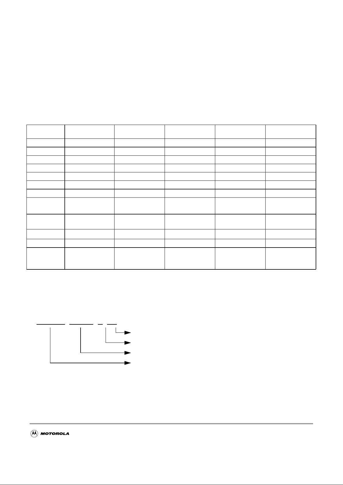
Derivative Differences and Document References
Derivative Differences
Table 0-1 shows the availability of peripheral modules on the various derivatives. For details about the
compatibility within the MC9S12D-Family refer also to engineering bulletin EB386.
The following figure provides an ordering number example for the MC9S12D128 devices.
Figure 0-1 Order Partnumber Example
The following items should be considered when using a derivative.
Table 0-1 Derivative Differences
1
NOTES:
1.
✓: Available for this device, ✕: Not available for this device
Modules
MC9S12DT128E,
MC9S12DT128
MC9S12DG128E,
MC9S12DG128
MC9S12DJ128E,
MC9S12DJ128
MC9S12DB128 MC9S12DB128
# of CANs 3 2220
CAN4 ✓✓✓✓✕
CAN1 ✓✕✕✕✕
CAN0 ✓✓✓✓✕
J1850/BDLC ✕✕✓✕✓
IIC ✓✓✓✕✕
Byteflight ✕✕✕✓✓
Package 112 LQFP
112 LQFP
80 QFP
2
112 LQFP
80 QFP
2
2. 80 Pin bond-out for MC9S12DG128E, MC9S12DG128, MC9S12DJ128E, and MC9S12DJ128 is the same, MC9S12DB128
has a different bond-out.
112 LQFP
80 QFP
2
Package
Code
PV PV/FU PV/FU PV FU
Mask set
1L40K3, 3L40K
3. Part numbers MC9S12DT128E, MC9S12DG128E, and MC9S12DJ128E are associated with the mark set 1L40K.
1L40K3, 3L40K 1L40K3, 3L40K
3L40K 3L40K
Temp Options M, V, C M, V, C M, V, C M, V, C M, V, C
Notes
An errata exists
contact Sales
Office
An errata exists
contact Sales
Office
An errata exists
contact Sales
Office
An errata exists
contact Sales
Office
An errata exists
contact Sales
Office
MC9S12 DJ128 C FU
Package Option
Temperature Option
Device Title
Controller Family
Temperature Options
C = -40˚C to 85˚C
V = -40˚C to 105˚C
M = -40˚C to 125˚C
Package Options
FU = 80QFP
PV = 112LQFP

MC9S12DT128 Device User Guide — V02.09
20
• Registers
– Do not write or read CAN0 registers (after reset: address range $0140 - $017F), if using a
derivative without CAN0 (see Table 0-1).
– Do not write or read CAN1 registers (after reset: address range $0180 - $01BF), if using a
derivative without CAN1 (see Table 0-1).
– Do not write or read CAN4 registers (after reset: address range $0280 - $02BF), if using a
derivative without CAN4 (see Table 0-1).
– Do not write or read BDLC registers (after reset: address range $00E8 - $00EF), if using a
derivative without BDLC (see Table 0-1).
– Do not write or read IIC registers (after reset: address range $00E0 - $00E7), if using a
derivative without IIC (see Table 0-1).
– Do not write or read Byteflight registers (after reset: address range $0300 - $035F), if using a
derivative without Byteflight registers (see Table 0-1).
• Interrupts
– Fill the four CAN0 interrupt vectors ($FFB0 - $FFB7) according to your coding policies for
unused interrupts, if using a derivative without CAN0 (see Table 0-1).
– Fill the four CAN1 interrupt vectors ($FFA8 - $FFAF) according to your coding policies for
unused interrupts, if using a derivative without CAN1 (see Table 0-1).
– Fill the four CAN4 interrupt vectors ($FF90 - $FF97) according to your coding policies for
unused interrupts, if using a derivative without CAN4 (see Table 0-1).
– Fill the BDLC interrupt vector ($FFC2, $FFC3) according to your coding policies for unused
interrupts, if using a derivative without BDLC (see Table 0-1).
– Fill the IIC interrupt vector ($FFC0, $FFC1) according to your coding policies for unused
interrupts, if using a derivative without IIC (see Table 0-1).
– Fill the fourByteflightinterrupt vectors ($FFA0 - $FFA7) according toyourcodingpolicies for
unused interrupts, if using a derivative without Byteflight (see Table 0-1).
• Ports
– The CAN0 pin functionality (TXCAN0, RXCAN0) is not available on port PJ7, PJ6, PM5,
PM4, PM3, PM2, PM1 and PM0, if using a derivative without CAN0 (see Table 0-1).
– The CAN1 pin functionality (TXCAN1, RXCAN1) is not available on port PM3 and PM2, if
using a derivative without CAN1 (see Table 0-1).
– The CAN4 pin functionality (TXCAN4, RXCAN4) is not available on port PJ7, PJ6, PM7,
PM6, PM5 and PM4, if using a derivative without CAN4 (see Table 0-1).
– The BDLC pin functionality (TXB, RXB) is not available on port PM1 and PM0, if using a
derivative without BDLC (see Table 0-1).
– The IIC pin functionality (SCL, SCA) is not available on port PJ7 and PJ6, if using a derivative
without IIC (see Table 0-1).

MC9S12DT128 Device User Guide — V02.09
21
– The Byteflight pin functionality (BF_PSLM, BF_PERR, BF_PROK, BF_PSYN, TX_BF,
RX_BF) is not available on port PM7, PM6, PM5, PM4, PM3 and PM2, if using a derivative
without Byteflight (see Table 0-1).
– Do not write MODRR1 and MODRR0 Bit of Module Routing Register (PIM_9DTB128Block
User Guide), if using a derivative without CAN0 (see Table 0-1).
– Do not write MODRR3 and MODRR2 Bit of Module Routing Register (PIM_9DTB128Block
User Guide), if using a derivative without CAN4 (see Table 0-1).
• Pins not available in 80 pin QFP package for MC9S12DG128E, MC9S12DG128,
MC9S12DJ128E, and MC9S12DJ128
– Port H
In order to avoid floating nodes the ports should be either configured as outputs by setting the
data direction register (DDRH at Base+$0262) to $FF, or enabling the pull resistors by writing
a $FF to the pull enable register (PERH at Base+$0264).
– Port J[1:0]
PortJpull-up resistors areenabled out ofreseton all fourpins(7:6 and 1:0).Therefore care must
be taken not to disable the pull enables on PJ[1:0] by clearing the bits PERJ1 and PERJ0 at
Base+$026C.
– Port K
Port K pull-up resistors are enabled out of reset, i.e. Bit 7 = PUKE = 1 in the register PUCR at
Base+$000C. Therefore care must be taken not to clear this bit.
– Port M[7:6]
PM7:6 must be configured as outputs or their pull resistors must be enabled to avoid floating
inputs.
– Port P6
PP6 must be configured as output or its pull resistor must be enabled to avoid a floating input.
– Port S[7:4]
PS7:4 must be configured as outputs or their pull resistors must be enabled to avoid floating
inputs.
– PAD[15:8] (ATD1 channels)
Out ofresetthe ATD1 is disabledpreventingcurrent flows in the pins.Donot modify the ATD1
registers!
• Pins not available in 80 pin QFP package for MC9S12DB128
– Port H
In order to avoid floating nodes the ports should be either configured as outputs by setting the
data direction register (DDRH at Base+$0262) to $FF, or enabling the pull resistors by writing
a $FF to the pull enable register (PERH at Base+$0264).
– Port J[7:6, 1:0]
PortJpull-up resistors areenabled out ofreseton all fourpins(7:6 and 1:0).Therefore care must
be taken not to disable the pull enables on PJ[7:6, 1:0] by clearing the bits PERJ7, PERJ6,
PERJ1 and PERJ0 at Base+$026C.
MC9S12DT128 Device User Guide — V02.09
22
– Port K
Port K pull-up resistors are enabled out of reset, i.e. Bit 7 = PUKE = 1 in the register PUCR at
Base+$000C. Therefore care must be taken not to clear this bit.
– Port M[1:0]
PM1:0 must be configured as outputs or their pull resistors must be enabled to avoid floating
inputs.
– Port P6
PP6 must be configured as output or its pull resistor must be enabled to avoid a floating input.
– Port S[3:2]
PS3:2 must be configured as outputs or their pull resistors must be enabled to avoid floating
inputs.
– PAD[15:8] (ATD1 channels)
Out ofresetthe ATD1 is disabledpreventingcurrent flows in the pins.Donot modify the ATD1
registers!
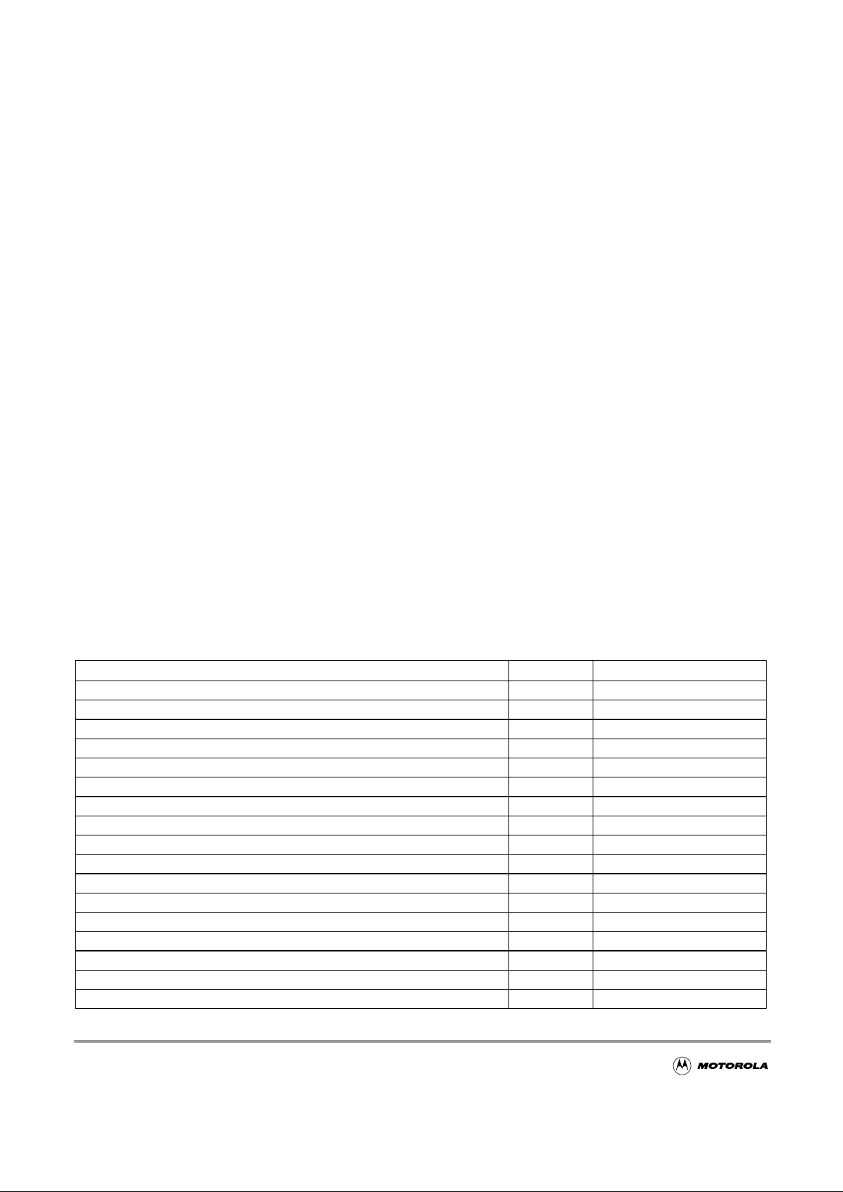
Document References
The Device User Guide provides information about the MC9S12DT128 device made up of standard
HCS12 blocks and the HCS12 processor core.
This document is part of the customer documentation. A complete set of device manuals also includes all
theindividualBlock User Guidesofthe implemented modules. Ina effort to reduceredundancy all module
specific information is located only in the respective Block User Guide. If applicable, special
implementation details of the module are given in the block description sections of this document.
See Table 0-2 for names and versions of the referenced documents throughout the Device User Guide.
Table 0-2 Document References
User Guide Version Document Order Number
HCS12 CPU Reference Manual V02 S12CPUV2/D
HCS12 Module Mapping Control (MMC) Block Guide V04 S12MMCV4/D
HCS12 Multiplexed External Bus Interface (MEBI) Block Guide V03 S12MEBIV3/D
HCS12 Interrupt (INT) Block Guide V01 S12INTV1/D
HCS12 Background Debug Module (BDM) Block Guide V04 S12BDMV4/D
HCS12 Breakpoint (BKP) Block Guide V01 S12BKPV1/D
Clock and Reset Generator (CRG) Block User Guide V04 S12CRGV4/D
Oscillator (OSC) Block User Guide V02 S12OSCV2/D
Enhanced Capture Timer 16 Bit 8 Channel (ECT_16B8C) Block User Guide V01 S12ECT16B8CV1/D
Analog to Digital Converter 10 Bit 8 Channel (ATD_10B8C) Block User Guide V02 S12ATD10B8CV2/D
Inter IC Bus (IIC) Block User Guide V02 S12IICV2/D
Asynchronous Serial Interface (SCI) Block User Guide V02 S12SCIV2/D
Serial Peripheral Interface (SPI) Block User Guide V02 S12SPIV2/D
Pulse Width Modulator 8 Bit 8 Channel (PWM_8B8C) Block User Guide V01 S12PWM8B8CV1/D
128K Byte Flash (FTS128K) Block User Guide V02 S12FTS128KV2/D
2K Byte EEPROM (EETS2K) Block User Guide V01 S12EETS2KV1/D
Byte Level Data Link Controller -J1850 (BDLC) Block User Guide V01 S12BDLCV1/D

MC9S12DT128 Device User Guide — V02.09
23
Motorola Scalable CAN (MSCAN) Block User Guide V02 S12MSCANV2/D
Voltage Regulator (VREG) Block User Guide V01 S12VREGV1/D
Port Integration Module (PIM_9DTB128) Block User Guide V02 S12DTB128PIMV2/D
Byteflight (BF) Block User Guide V01 S12BFV1/D
User Guide Version Document Order Number

MC9S12DT128 Device User Guide — V02.09
24

MC9S12DT128 Device User Guide — V02.09
25
Section 1 Introduction
1.1 Overview
The MC9S12DT128 microcontroller unit (MCU) is a 16-bit device composed of standard on-chip
peripherals including a 16-bit central processing unit (HCS12 CPU), 128K bytes of Flash EEPROM, 8K
bytes of RAM, 2K bytes of EEPROM, two asynchronous serial communications interfaces (SCI), two
serial peripheral interfaces (SPI), an 8-channel IC/OC enhanced capture timer, two 8-channel, 10-bit
analog-to-digital converters(ADC),an 8-channel pulse-width modulator(PWM),a digital Byte Data Link
Controller (BDLC), 29 discrete digital I/O channels (Port A, Port B, Port K and Port E), 20 discrete digital
I/O lines with interrupt and wakeup capability, three CAN 2.0 A, B software compatible modules
(MSCAN12), a Byteflight module and an Inter-IC Bus. The MC9S12DT128 has full 16-bit data paths
throughout. However, the external bus can operate in an 8-bit narrow mode so single 8-bit wide memory
can be interfaced for lower cost systems. The inclusion of a PLL circuit allows power consumption and
performance to be adjusted to suit operational requirements.
1.2 Features
• HCS12 Core
– 16-bit HCS12 CPU
i. Upward compatible with M68HC11 instruction set
ii. Interrupt stacking and programmer’s model identical to M68HC11
iii.20-bit ALU
iv.Instruction queue
v. Enhanced indexed addressing
– MEBI (Multiplexed External Bus Interface)
– MMC (Module Mapping Control)
– INT (Interrupt control)
– BKP (Breakpoints)
– BDM (Background Debug Module)
• CRG (Clock and Reset Generator)
– Choice of low current Colpitts oscillator or standard Pierce Oscillator
– PLL
– COP watchdog
– real time interrupt
– clock monitor
• 8-bit and 4-bit ports with interrupt functionality

MC9S12DT128 Device User Guide — V02.09
26
– Digital filtering
– Programmable rising or falling edge trigger
• Memory
– 128K Flash EEPROM
– 2K byte EEPROM
– 8K byte RAM
• Two 8-channel Analog-to-Digital Converters
– 10-bit resolution
– External conversion trigger capability
• Three 1M bit per second, CAN 2.0 A, B software compatible modules
– Five receive and three transmit buffers
– Flexible identifier filter programmable as 2 x 32 bit, 4 x 16 bit or 8x8bit
– Four separate interrupt channels for Rx, Tx, error and wake-up
– Low-pass filter wake-up function
– Loop-back for self test operation
• Enhanced Capture Timer
– 16-bit main counter with 7-bit prescaler
– 8 programmable input capture or output compare channels
– Four 8-bit or two 16-bit pulse accumulators
• 8 PWM channels
– Programmable period and duty cycle
– 8-bit 8-channel or 16-bit 4-channel
– Separate control for each pulse width and duty cycle
– Center-aligned or left-aligned outputs
– Programmable clock select logic with a wide range of frequencies
– Fast emergency shutdown input
– Usable as interrupt inputs
• Serial interfaces
– Two asynchronous Serial Communications Interfaces (SCI)
– Two Synchronous Serial Peripheral Interface (SPI)
– Byteflight
• Byte Data Link Controller (BDLC)

MC9S12DT128 Device User Guide — V02.09
27
• SAE J1850 Class B Data Communications Network Interface
– Compatible and ISO Compatible for Low-Speed (<125 Kbps) Serial Data Communications in
Automotive Applications
• Inter-IC Bus (IIC)
– Compatible with I2C Bus standard
– Multi-master operation
– Software programmable for one of 256 different serial clock frequencies
• 112-Pin LQFP and 80-Pin QFP package options
– I/O lines with 5V input and drive capability
– 5V A/D converter inputs
– Operation at 50MHz equivalent to 25MHz Bus Speed
– Development support
– Single-wire background debug™ mode
– On-chip hardware breakpoints
1.3 Modes of Operation
User modes
• Normal and Emulation Operating Modes
– Normal Single-Chip Mode
– Normal Expanded Wide Mode
– Normal Expanded Narrow Mode
– Emulation Expanded Wide Mode
– Emulation Expanded Narrow Mode
• Special Operating Modes
– Special Single-Chip Mode with active Background Debug Mode
– Special Test Mode (Motorola use only)
– Special Peripheral Mode (Motorola use only)
Low power modes
• Stop Mode
• Pseudo Stop Mode
• Wait Mode

MC9S12DT128 Device User Guide — V02.09
28
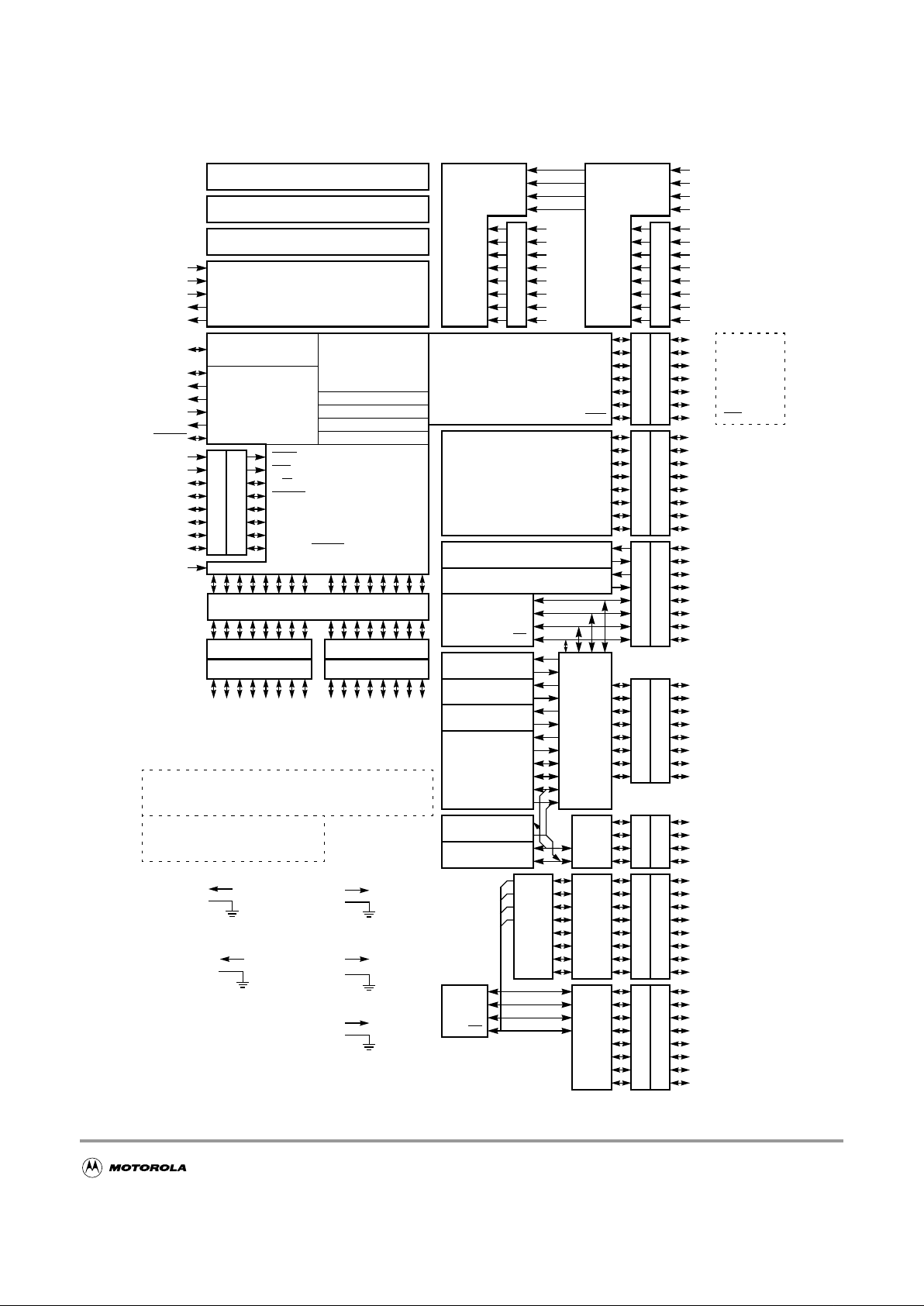
1.4 Block Diagram
Figure 1-1 shows a block diagram of the MC9S12DT128 device.
MC9S12DT128 Device User Guide — V02.09
29
Figure 1-1 MC9S12DT128 Block Diagram
128K Byte Flash EEPROM
8K Byte RAM
Enhanced Capture
RESET
EXTAL
XTAL
V
DD1,2
V
SS1,2
SCI0
2K Byte EEPROM
BKGD
R/
W
MODB
XIRQ
NOACC/
XCLKS
System
Integration
Module
(SIM)
VDDR
CPU
Periodic Interrupt
COP Watchdog
Clock Monitor
Single-wire Background
Breakpoints
PLL
VSSPLL
XFC
VDDPLL
Multiplexed Address/Data Bus
VDDA
VSSA
VRH
VRL
ATD0
Multiplexed
Wide Bus
Multiplexed
V
DDX
V
SSX
Internal Logic 2.5V
Narrow Bus
PPAGE
V
DDPLL
V
SSPLL
PLL 2.5V
IRQ
LSTRB
ECLK
MODA
PA4
PA3
PA2
PA1
PA0
PA7
PA6
PA5
TEST
ADDR12
ADDR11
ADDR10
ADDR9
ADDR8
ADDR15
ADDR14
ADDR13
DATA12
DATA11
DATA10
DATA9
DATA8
DATA15
DATA14
DATA13
PB4
PB3
PB2
PB1
PB0
PB7
PB6
PB5
ADDR4
ADDR3
ADDR2
ADDR1
ADDR0
ADDR7
ADDR6
ADDR5
DATA4
DATA3
DATA2
DATA1
DATA0
DATA7
DATA6
DATA5
DATA4
DATA3
DATA2
DATA1
DATA0
DATA7
DATA6
DATA5
PE3
PE4
PE5
PE6
PE7
PE0
PE1
PE2
AN2
AN6
AN0
AN7
AN1
AN3
AN4
AN5
PAD03
PAD04
PAD05
PAD06
PAD07
PAD00
PAD01
PAD02
IOC2
IOC6
IOC0
IOC7
IOC1
IOC3
IOC4
IOC5
PT3
PT4
PT5
PT6
PT7
PT0
PT1
PT2
VRH
VRL
VDDA
VSSA
VRH
VRL
ATD1
AN2
AN6
AN0
AN7
AN1
AN3
AN4
AN5
PAD11
PAD12
PAD13
PAD14
PAD15
PAD08
PAD09
PAD10
VDDA
VSSA
RXD
TXD
MISO
MOSI
PS3
PS4
PS5
PS0
PS1
PS2
SCI1
RXD
TXD
PWM2
PWM6
PWM0
PWM7
PWM1
PWM3
PWM4
PWM5
PP3
PP4
PP5
PP6
PP7
PP0
PP1
PP2
PIX2
PIX0
PIX1
PIX3
ROMCTL
ECS
PK3
PK7
PK0
PK1
XADDR17
ECS ROMCTL
XADDR14
XADDR15
XADDR16
SCK
SS
PS6
PS7
SPI0
IIC
SDA
SCL
PJ6
PJ7
CAN0
RxCAN
TxCAN
PM1
PM0
CAN1
RxCAN
TxCAN
PM2
PM3
PM4
PM5
PM6
PM7
KWH2
KWH6
KWH0
KWH7
KWH1
KWH3
KWH4
KWH5
PH3
PH4
PH5
PH6
PH7
PH0
PH1
PH2
KWJ0
KWJ1
PJ0
PJ1
I/O Driver 5V
V
DDA
V
SSA
A/D Converter 5V &
DDRA DDRB
PTA PTB
DDRE
PTE
AD1
AD0
PTK
DDRK
PTT
DDRT
PTP
DDRP
PTS
DDRS
PTM
DDRM
PTH
DDRH
PTJ
DDRJ
PK2
BDLC
RxB
TxB
Clock and
Reset
Generation
Module
Voltage Regulator
VSSR
Debug Module
VDD1,2
VSS1,2
VREGEN
V
DDR
V
SSR
Voltage Regulator 5V & I/O
CAN0,4
RxCAN
TxCAN
MISO
MOSI
SCK
SS
SPI1
PIX4
PIX5
PK4
PK5
XADDR18
XADDR19
Voltage Regulator Reference
KWP2
KWP6
KWP0
KWP7
KWP1
KWP3
KWP4
KWP5
KWJ6
KWJ7
Timer
(J1850)
Signals shown in Bold are not available in any of the two the 80 Pin Package Options
Module to Port Routing
RX_BF
TX_BF
BYTE-
BF_PSYN
BF_PROK
BF_PERR
BF_PSLM
FLIGHT
Signals shown in
Bold-Italics
are not available in the 80 Pin Package Option for DG and DJ128
Signals shown in
Italics
are not available in the 80 Pin Package Option for B128
MC9S12DT128 Device User Guide — V02.09
30
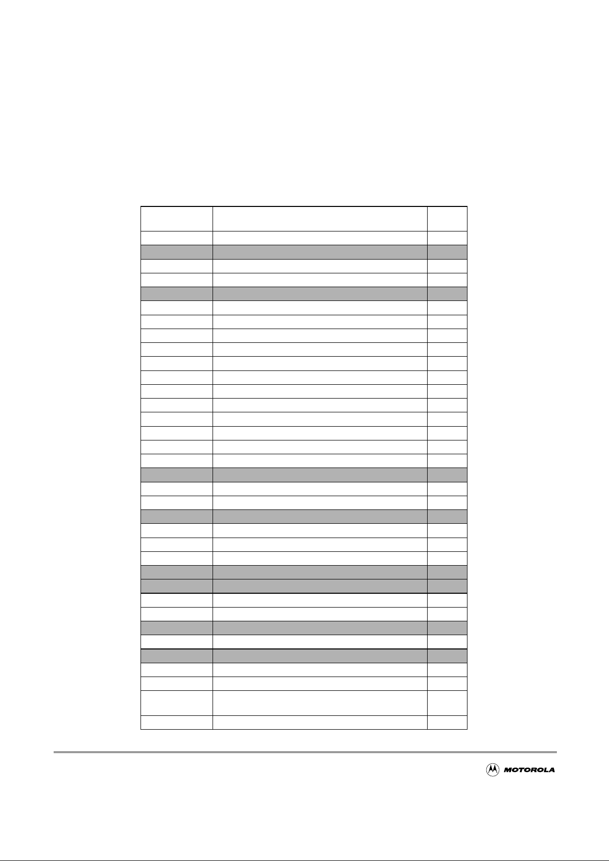
1.5 Device Memory Map
Table 1-1andFigure 1-2 showthedevice memory mapofthe MC9S12DT128afterreset. Note thatafter
reset the EEPROM ($0000
– $07FF) is hidden by the register space ($0000 - $03FF) and the RAM ($0000
- $1FFF). The bottom 1K Bytes of RAM ($0000 - $03FF) are hidden by the register space.
Table 1-1 Device Memory Map
Address Module
Size
(Bytes)
$0000 – $0017 CORE (Ports A, B, E, Modes, Inits, Test) 24
$0018 – $0019 Reserved 2
$001A – $001B Device ID register (PARTID) 2
$001C – $001F CORE (MEMSIZ, IRQ, HPRIO) 4
$0020 – $0027 Reserved 8
$0028 – $002F CORE (Background Debug Module) 8
$0030 – $0033 CORE (PPAGE, Port K) 4
$0034 – $003F Clock and Reset Generator (PLL, RTI, COP) 12
$0040 – $007F Enhanced Capture Timer 16-bit 8 channels 64
$0080 – $009F Analog to Digital Converter 10-bit 8 channels (ATD0) 32
$00A0 – $00C7 Pulse Width Modulator 8-bit 8 channels (PWM) 40
$00C8 – $00CF Serial Communications Interface (SCI0) 8
$00D0 – $00D7 Serial Communications Interface (SCI1) 8
$00D8 – $00DF Serial Peripheral Interface (SPI0) 8
$00E0 – $00E7 Inter IC Bus 8
$00E8 – $00EF Byte Level Data Link Controller (BDLC) 8
$00F0 – $00F7 Serial Peripheral Interface (SPI1) 8
$00F8 – $00FF Reserved 8
$0100 – $010F Flash Control Register 16
$0110 – $011B EEPROM Control Register 12
$011C – $011F Reserved 4
$0120 – $013F Analog to Digital Converter 10-bit 8 channels (ATD1) 32
$0140 – $017F Motorola Scalable CAN (CAN0) 64
$0180 – $01BF Motorola Scalable CAN (CAN1) 64
$01C0 – $01FF Reserved 64
$0200 – $023F Reserved 64
$0240 – $027F Port Integration Module (PIM) 64
$0280 – $02BF Motorola Scalable CAN (CAN4) 64
$02C0 – $02FF Reserved 64
$0300 – $035F Byteflight (BF) 96
$0360 – $03FF Reserved 160
$0000 – $07FF EEPROM array 2048
$0000 – $1FFF RAM array 8192
$4000 – $7FFF
Fixed Flash EEPROM array
incl. 0.5K, 1K, 2K or 4K Protected Sector at start
16384
$8000 – $BFFF Flash EEPROM Page Window 16384
 Loading...