

查询MC88915供应商
SEMICONDUCTOR TECHNICAL DATA
"' '
" #&#$ %%
! ( #$"!$
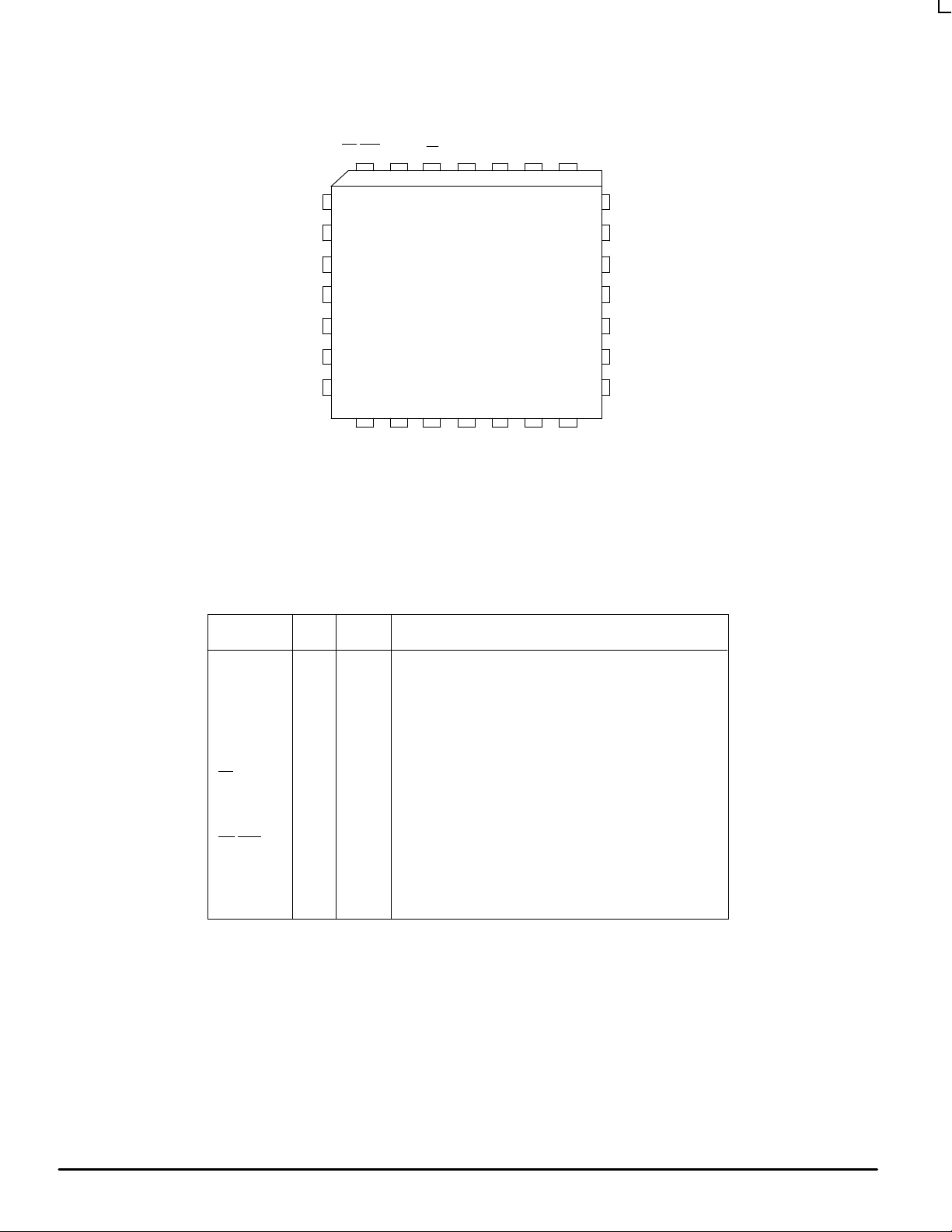
The MC88915T Clock Driver utilizes phase–locked loop technology to
lock its low skew outputs’ frequency and phase onto an input reference
clock. It is designed to provide clock distribution for high performance
PC’s and workstations. For a 3.3V version, see the MC88LV915T data
sheet.
The PLL allows the high current, low skew outputs to lock onto a single
clock input and distribute it with essentially zero delay to multiple
components on a board. The PLL also allows the MC88915T to multiply a
low frequency input clock and distribute it locally at a higher (2X) system
frequency . Multiple 88915’ s can lock onto a single reference clock, which
is ideal for applications when a central system clock must be distributed
synchronously to multiple boards (see Figure 7).
Five “Q” outputs (Q0–Q4) are provided with less than 500 ps skew between their rising edges. The Q5
phase shift) from the “Q” outputs. The 2X_Q output runs at twice the “Q” output frequency, while the Q/2 runs at 1/2 the “Q”
frequency.
The VCO is designed to run optimally between 20 MHz and the 2X_Q F
the different feedback configurations which create specific input/output frequency relationships. Possible frequency ratios of the
“Q” outputs to the SYNC input are 2:1, 1:1, and 1:2.
The FREQ_SEL pin provides one bit programmable divide–by in the feedback path of the PLL. It selects between divide–by–1
and divide–by–2 of the VCO before its signal reaches the internal clock distribution section of the chip (see the block diagram on
page 2). In most applications FREQ_SEL should be held high (÷1). If a low frequency reference clock input is used, holding
FREQ_SEL low (÷2) will allow the VCO to run in its optimal range (>20MHz and >40MHz for the TFN133 version).
In normal phase–locked operation the PLL_EN pin is held high. Pulling the PLL_EN pin low disables the VCO and puts the 88915
in a static “test mode”. In this mode there is no frequency limitation on the input clock, which is necessary for a low frequency board
test environment. The second SYNC input can be used as a test clock input to further simplify board–level testing (see detailed
description on page 1 1).
Pulling the OE
/RST pin goes back high Q0–Q4, Q5 and Q/2 will be reset in the low state, with 2X_Q being the inverse of the selected SYNC
OE
input. Assuming PLL_EN is low, the outputs will remain reset until the 88915 sees a SYNC input pulse.
A lock indicator output (LOCK) will go high when the loop is in steady–state phase and frequency lock. The LOCK output will go
low if phase–lock is lost or when the PLL_EN pin is low. The LOCK output will go high no later than 10ms after the 88915 sees a
SYNC signal and full 5V VCC.
/RST pin low puts the clock outputs 2X_Q, Q0–Q4, Q5 and Q/2 into a high impedance state (3–state). After the
max
LOW SKEW CMOS
PLL CLOCK DRIVER
output is inverted (180°
specification. The wiring diagrams in Figure 5 detail
Features
•
Five Outputs (Q0–Q4) with Output–Output Skew < 500 ps each being phase and frequency locked to the SYNC input
• The phase variation from part–to–part between the SYNC and FEEDBACK inputs is less than 550 ps (derived from the t
specification, which defines the part–to–part skew)
• Input/Output phase–locked frequency ratios of 1:2, 1:1, and 2:1 are available
• Input frequency range from 5MHz – 2X_Q FMAX spec. (10MHz – 2X_Q FMAX for the TFN133 version)
• Additional outputs available at 2X and +2 the system “Q” frequency. Also a Q (180° phase shift) output available
• All outputs have ±36 mA drive (equal high and low) at CMOS levels, and can drive either CMOS or TTL inputs. All inputs
are TTL–level compatible. ±88mA IOL/IOH specifications guarantee 50Ω transmission line switching on the incident edge
• Test Mode pin (PLL_EN) provided for low frequency testing. Two selectable CLOCK inputs for test or redundancy purposes.
All outputs can go into high impedance (3–state) for board test purposes
• Lock Indicator (LOCK) accuracy indicates a phase–locked state
Yield Surface Modeling and YSM are trademarks of Motorola, Inc.
1/97
Motorola, Inc. 1997
1
REV 4
PD
MC88915TFN55/70/100/133/160
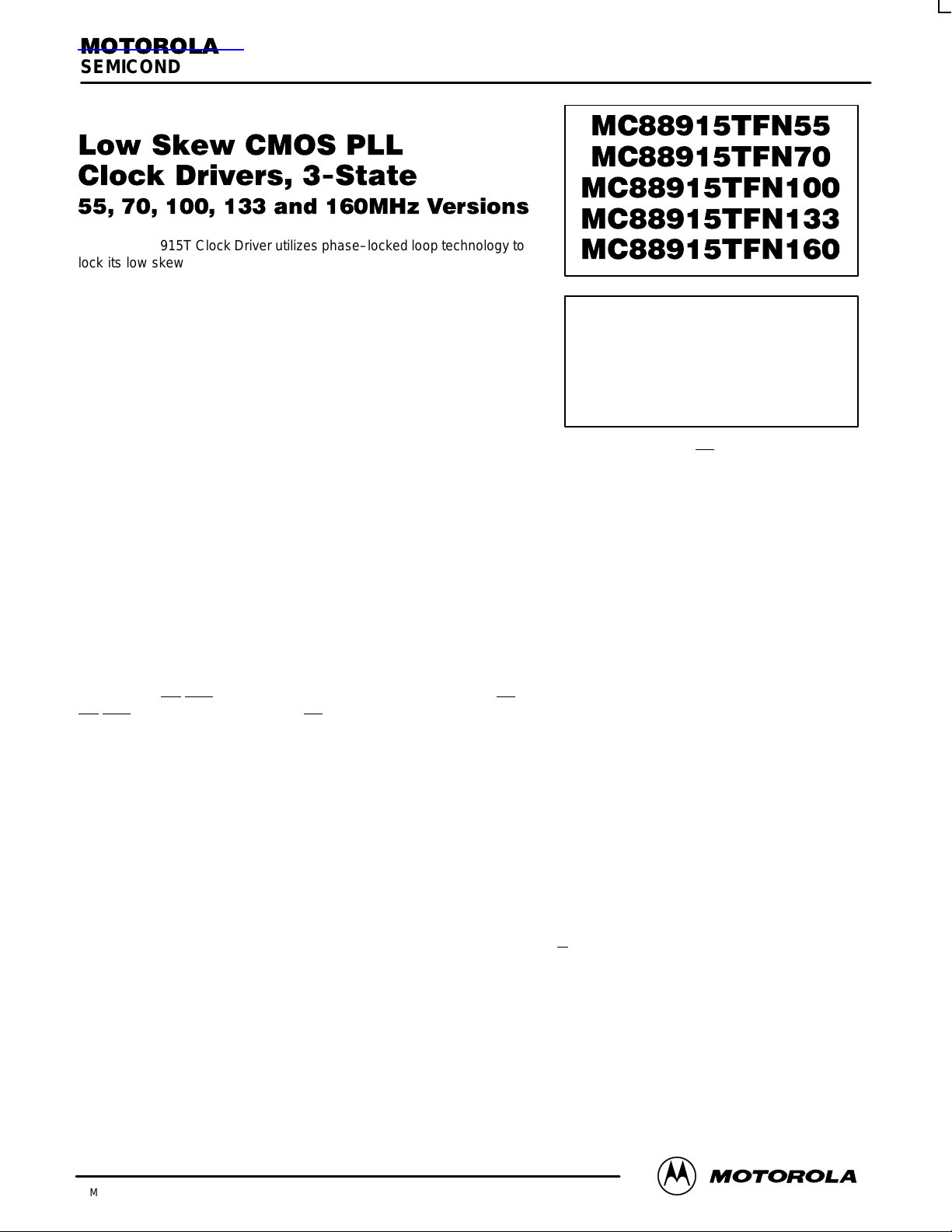
Pinout: 28–Lead PLCC (Top View)
FEEDBACK
REF_SEL
SYNC[0]
VCC(AN)
RC1
GND(AN)
SYNC[1]
PIN SUMMARY
/RST V
5
6
7
8
9
10
FREQ_SEL
CC
Q0GND
FN SUFFIX
PLASTIC PLCC
CASE 776–02
CC
2X_QOE
V
Q4Q5 GND
CC
2627284321
Q/2
25
GND
24
Q3
23
V
22
CC
Q2
21
GND
20
LOCK
1911
18171612 13 14 15
PLL_ENGNDQ1V
Pin Name Num I/O Function
1
SYNC[0]
SYNC[1]
REF_SEL
FREQ_SEL
FEEDBACK
RC1
Q(0–4)
Q5
2x_Q
Q/2
LOCK
OE
/RST
PLL_EN
VCC,GND
11
Input
1
Input
1
Input
1
Input
1
Input
1
Input
5
Output
1
Output
1
Output
1
Output
1
Output
1
Input
1
Input
Reference clock input
Reference clock input
Chooses reference between sync[0] & Sync[1]
Doubles VCO Internal Frequency (low)
Feedback input to phase detector
Input for external RC network
Clock output (locked to sync)
Inverse of clock output
2 x clock output (Q) frequency (synchronous)
Clock output(Q) frequency
÷
2 (synchronous)
Indicates phase lock has been achieved (high when locked)
Output Enable/Asynchronous reset (active low)
Disables phase–lock for low freq. testing
Power and ground pins (note pins 8, 10 are
“analog” supply pins for internal PLL only)
MOTOROLA TIMING SOLUTIONS
2
BR1333 — Rev 6
FEEDBACK
MC88915TFN55/70/100/133/160
LOCK
SYNC (0)
SYNC (1)
REF_SEL
PLL_EN
FREQ_SEL
OE/RST
0
M
U
X
1
PHASE/FREQ.
DETECTOR
1
0
MUX
DIVIDE
BY TWO
CHARGE PUMP/LOOP
FILTER
EXTERNAL REC NETWORK
(RC1 Pin)
÷
1)
(
1
M
(
÷
2)
U
X
0
VOLTAGE
CONTROLLED
OSCILLA TOR
D
Q
CP
Q
R
D
Q
CP
R
D
Q
CP
R
2x_Q
Q0
Q1
Q2
MC88915T Block Diagram (All Versions)
D
CP
D
CP
D
CP
D
CP
Q
R
Q
R
Q
R
Q
R
Q3
Q4
Q5
Q/2
TIMING SOLUTIONS
BR1333 — Rev 6
3 MOTOROLA
MC88915TFN55/70/100/133/160
MC88915TFN55 and MC88915TFN70
SYNC INPUT TIMING REQUIREMENTS
Minimum
Symbol Parameter TFN70 TFN55 Maximum Unit
t
RISE/FALL
t
CYCLE
Duty Cycle SYNC Inputs Input Duty Cycle SYNC Inputs 50% ±25%
1. These t
in Figure 5b.
2. Information in Table 1 and in Note 3 of the AC specification notes describe this specification and its limits depending on what output is fed back,
and if FREQ_SEL is high or low.
DC ELECTRICAL CHARACTERISTICS
(Voltages Referenced to GND) TA =–40° C to +85° C for 55MHz Version; TA =0° C to +70° C for 70MHz Version; VCC = 5.0 V ± 5%
Symbol
V
V
V
OH
V
I
I
CCT
I
OLD
I
OHD
I
CC
I
OZ
1. IOL and IOH are 12mA and –12mA respectively for the LOCK output.
2. The PLL_EN input pin is not guaranteed to meet this specification.
3. Maximum test duration is 2.0ms, one output loaded at a time.
4. Specification value for IOZ is preliminary, will be finalized upon ‘MC’ status.
,SYNC Inputs Rise/Fall Time, SYNC Inputs
, SYNC Inputs Input Clock Period SYNC Inputs 28.5
minimum values are valid when ‘Q’ output is fed back and connected to the FEEDBACK pin. This is the configuration shown
CYCLE
Minimum High–Level Input
IH
Voltage
Maximum Low–Level Input
IL
Voltage
Minimum High–Level Output
Voltage
OL
Maximum Low–Level Output
Voltage
Maximum Input Leakage Current VI = VCC or GND 5.25 ±1.0 µA
in
Maximum ICC/Input VI = VCC – 2.1 V 5.25
Minimum Dynamic Output Current
Maximum Quiescent Supply
Current (per Package)
Maximum 3–State Leakage Current VI = VIH or VIL;VO = VCC or GND 5.25 ±50
From 0.8 to 2.0V
Parameter Test Conditions
V
= 0.1 V or VCC – 0.1 V 4.75
out
V
= 0.1 V or VCC – 0.1 V 4.75
out
Vin = VIH or V
IOH = –36 mA
Vin = VIH or V
IOL = 36 mA
3
V
OLD
V
OHD
VI = VCC or GND 5.25 1.0 mA
IL
1
IL
1
= 1.0V Max 5.25 88 mA
= 3.85V Min 5.25 –88 mA
— — 3.0 ns
V
CC
V
5.25
5.25
4.75
5.25
4.75
5.25
1
1
36.0
Target Limit Unit
2.0
2.0
0.8
0.8
4.01
4.51
0.44
0.44
2.0
200
2
4
2
ns
mA
µA
V
V
V
V
CAPACITANCE AND POWER SPECIFICATIONS
Symbol Parameter Typical Values Unit Conditions
C
IN
C
PD
PD
1
PD
2
NOTE: PD1 and PD2 mW/Output numbers are for a ‘Q’ output.
FREQUENCY SPECIFICATIONS (T
Symbol Parameter TFN70 TFN55 Unit
1
f
max
1. Maximum Operating Frequency is guaranteed with the part in a phase–locked condition, and all outputs loaded with 50Ω terminated to VCC/2.
MOTOROLA TIMING SOLUTIONS
Input Capacitance 4.5 pF VCC = 5.0 V
Power Dissipation Capacitance 40 pF VCC = 5.0 V
Power Dissipation @ 50MHz with 50Ω Thevenin Termination 23mW/Output
Power Dissipation @ 50MHz with 50Ω Parallel Termination to GND 57mW/Output
=–40° C to +85° C, VCC = 5.0 V ±5%)
A
Maximum Operating Frequency (2X_Q Output) 70 55 MHz
Maximum Operating Frequency (Q0–Q4,Q5 Output) 35 27.5 MHz
4
184mW/Device
456mW/Device
Guaranteed Minimum
mW VCC = 5.0 V
T = 25°C
mW VCC = 5.0 V
T = 25° C
BR1333 — Rev 6
MC88915TFN55/70/100/133/160
1,3
Cpu s)
pa a o
MC88915TFN55 and MC88915TFN70 (continued)
AC CHARACTERISTICS (T
Symbol
t
RISE/FALL
Outputs
t
RISE/FALL
2X_Q Output
t
PULSE WIDTH
(Q0–Q4, Q5
t
PULSE WIDTH
(2X_Q Output)
t
PULSE WIDTH
(2X_Q Output)
t
PD
SYNC Feedback (Measured at SYNC0 or 1 and
t
SKEWr
(Rising) See Note
t
SKEWf
(Falling)
t
SKEWall
t
LOCK
t
PZL
t
PHZ,tPLZ
1. These specifications are not tested, they are guaranteed by statistcal characterization. See AC specification Note 1.
2. T
CYCLE
3. The TPD specification’s min/max values may shift closer to zero if a larger pullup resistor is used.
4. Under equally loaded conditions and at a fixed temperature and voltage.
5. With VCC fully powered–on, and an output properly connected to the FEEDBACK pin. t
with C1 = 0.01µF.
6. The t
reached.
1
1
, Q/2)
1
1
1,4
1,4
1,4
5
6
PZL
5
6
in this spec is 1/Frequency at which the particular output is running.
, t
, t
PHZ
PLZ
=–40° C to +85° C, VCC = 5.0V ±5%, Load = 50Ω Terminated to VCC/2)
A
Parameter Min Max Unit Condition
Rise/Fall Time, All Outputs
(Between 0.2VCC and 0.8VCC)
Rise/Fall Time Into a 20pF Load, With
Termination Specified in Note
Output Pulse Width: Q0, Q1, Q2, Q3,
Q4, Q5
, Q/2 @ VCC/2
Output Pulse Width: 66MHz
2X_Q @ 1.5V 50MHz
Output Pulse Width: 50–65MHz
2X_Q @ VCC/2 40–49MHz
SYNC Input to Feedback Delay
FEEDBACK Input Pins)
Output–to–Output Skew Between Outputs Q0–Q4, Q/2 (Rising Edges Only)
Output–to–Output Skew Between Outputs Q0–Q4 (Falling Edges Only)
Output–to–Output Skew 2X_Q, Q/2,
Q0–Q4 Rising, Q5 Falling
Time Required to Acquire Phase–Lock
From Time SYNC Input Signal is
Received
Output Enable Time OE/RST to 2X_Q,
Q0–Q4, Q5
Output Disable Time OE/RST to 2X_Q,
Q0–Q4, Q5
minimum and maximum specifications are estimates, the final guaranteed values will be available when ‘MC’ status is
, and Q/2
, and Q/2
2
40MHz
66–70MHz
1.0 2.5 ns Into a 50Ω Load
0.5 1.6 ns t
0.5t
0.5t
0.5t
0.5t
0.5t
0.5t
0.5t
– 0.520.5t
CYCLE
– 0.5
CYCLE
CYCLE
(With 1MΩ from RC1 to An GND)
– 1.0
CYCLE
– 1.5
CYCLE
– 1.0
– 1.5
CYCLE
– 0.5
CYCLE
(With 1MΩ from RC1 to An VCC)
–1.05 –0.40
+1.25 +3.25
— 500 ps All Outputs Into a
— 500 ps All Outputs Into a
— 750 ps All Outputs Into a
1.0 10 ms Also Time to LOCK
3.0 14 ns Measured With the
3.0 14 ns Measured With the
CYCLE
2
0.5t
CYCLE
0.5t
CYCLE
0.5t
CYCLE
2
0.5t
CYCLE
0.5t
CYCLE
0.5t
CYCLE
maximum is with C1 = 0.1µF, t
LOCK
+ 0.5
+ 0.5
+ 1.0
+ 1.5
+ 1.0
+ 1.5
+ 0.5
2
ns Into a 50Ω Load
2
ns Must Use Termination
2
ns Into a 50Ω Load
ns See Note 4 and
Terminated to VCC/2
: 0.8V – 2.0V
RISE
t
: 2.0V – 0.8V
FALL
Terminated to VCC/2
Specified in Note 2
Terminated to VCC/2
Figure 2 for Detailed
Explanation
Matched 50Ω Load
Terminated to VCC/2
Matched 50Ω Load
Terminated to VCC/2
Matched 50Ω Load
Terminated to VCC/2
Indicator High
PLL_EN Pin Low
PLL_EN Pin Low
minimum is
LOCK
TIMING SOLUTIONS
BR1333 — Rev 6
5 MOTOROLA
MC88915TFN55/70/100/133/160
MC88915TFN100
SYNC INPUT TIMING REQUIREMENTS
Symbol Parameter Minimum Maximum Unit
t
RISE/FALL
t
CYCLE
Duty Cycle SYNC Inputs Input Duty Cycle SYNC Inputs 50% ±25%
1. These t
in Figure 5b.
2. Information in Table 1 and in Note 3 of the AC specification notes describe this specification and its limits depending on what output is fed back,
and if FREQ_SEL is high or low.
,SYNC Inputs Rise/Fall Time, SYNC Inputs From 0.8 to 2.0V — 3.0 ns
, SYNC Inputs Input Clock Period SYNC Inputs 20.0
minimum values are valid when ‘Q’ output is fed back and connected to the FEEDBACK pin. This is the configuration shown
CYCLE
1
200
2
ns
DC ELECTRICAL CHARACTERISTICS (Voltages Referenced to GND) T
Symbol
V
V
V
OH
V
OL
I
I
CCT
I
OLD
I
OHD
I
CC
I
OZ
1. IOL and IOH are 12mA and –12mA respectively for the LOCK output.
2. The PLL_EN input pin is not guaranteed to meet this specification.
3. Maximum test duration is 2.0ms, one output loaded at a time.
4. Specification value for IOZ is preliminary, will be finalized upon ‘MC’ status.
Minimum High–Level Input
IH
Voltage
Maximum Low–Level Input
IL
Voltage
Minimum High–Level Output
Voltage
Maximum Low–Level Output
Voltage
Maximum Input Leakage Current VI = VCC or GND 5.25 ±1.0 µA
in
Maximum ICC/Input VI = VCC – 2.1 V 5.25
Minimum Dynamic Output Current
Maximum Quiescent Supply
Current (per Package)
Maximum 3–State Leakage Current VI = VIH or VIL;VO = VCC or GND 5.25 ±50
Parameter Test Conditions
V
= 0.1 V or VCC – 0.1 V 4.75
out
V
= 0.1 V or VCC – 0.1 V 4.75
out
Vin = VIH or V
IOH = –36 mA
Vin = VIH or V
IOL = 36 mA
3
V
= 1.0V Max 5.25 88 mA
OLD
V
= 3.85V Min 5.25 –88 mA
OHD
VI = VCC or GND 5.25 1.0 mA
=–40° C to +85° C, VCC = 5.0 V ± 5%
A
V
CC
V
5.25
5.25
IL
1
IL
1
4.75
5.25
4.75
5.25
Target Limit Unit
2.0
2.0
0.8
0.8
4.01
4.51
0.44
0.44
2
2.0
4
CAPACITANCE AND POWER SPECIFICATIONS
Symbol Parameter Typical Values Unit Conditions
C
IN
C
PD
PD
1
PD
2
NOTE: PD1 and PD2 mW/Output numbers are for a ‘Q’ output.
Input Capacitance 4.5 pF VCC = 5.0 V
Power Dissipation Capacitance 40 pF VCC = 5.0 V
Power Dissipation @ 50MHz with 50Ω Thevenin Termination 23mW/Output
184mW/Device
Power Dissipation @ 50MHz with 50Ω Parallel Termination to GND 57mW/Output
456mW/Device
mW VCC = 5.0 V
mW VCC = 5.0 V
V
V
V
V
mA
µA
T = 25°C
T = 25° C
FREQUENCY SPECIFICATIONS (T
Symbol Parameter TFN100 Unit
1
f
max
1. Maximum Operating Frequency is guaranteed with the part in a phase–locked condition, and all outputs loaded with 50Ω terminated to VCC/2.
MOTOROLA TIMING SOLUTIONS
Maximum Operating Frequency (2X_Q Output) 100 MHz
Maximum Operating Frequency (Q0–Q4,Q5 Output) 50 MHz
=–40° C to +85° C, VCC = 5.0 V ±5%)
A
6
Guaranteed Minimum
BR1333 — Rev 6

MC88915TFN55/70/100/133/160
1,3
Cpu s)
pa a o
MC88915TFN100 (continued)
AC CHARACTERISTICS (T
Symbol
t
RISE/FALL
Outputs
t
RISE/FALL
2X_Q Output
t
PULSE WIDTH
(Q0–Q4, Q5
t
PULSE WIDTH
(2X_Q Output)
t
PULSE WIDTH
(2X_Q Output)
t
PD
SYNC Feedback (Measured at SYNC0 or 1 and
t
SKEWr
(Rising) See Note
t
SKEWf
(Falling)
t
SKEWall
t
LOCK
t
PZL
t
PHZ,tPLZ
1. These specifications are not tested, they are guaranteed by statistcal characterization. See AC specification Note 1.
2. T
CYCLE
3. The TPD specification’s min/max values may shift closer to zero if a larger pullup resistor is used.
4. Under equally loaded conditions and at a fixed temperature and voltage.
5. With VCC fully powered–on, and an output properly connected to the FEEDBACK pin. t
with C1 = 0.01µF.
6. The t
reached.
1
1
, Q/2)
1
1
1,4
1,4
1,4
5
6
PZL
5
6
in this spec is 1/Frequency at which the particular output is running.
, t
, t
PHZ
PLZ
=–40° C to +85° C, VCC = 5.0V ±5%, Load = 50Ω Terminated to VCC/2)
A
Parameter Min Max Unit Condition
Rise/Fall Time, All Outputs
(Between 0.2VCC and 0.8VCC)
Rise/Fall Time Into a 20pF Load, With
Termination Specified in Note
Output Pulse Width: Q0, Q1, Q2, Q3,
Q4, Q5
, Q/2 @ VCC/2
Output Pulse Width:
2X_Q @ 1.5V
Output Pulse Width: 40–49MHz
2X_Q @ VCC/2 50–65MHz
SYNC Input to Feedback Delay
FEEDBACK Input Pins)
Output–to–Output Skew Between Outputs Q0–Q4, Q/2 (Rising Edges Only)
Output–to–Output Skew Between Outputs Q0–Q4 (Falling Edges Only)
Output–to–Output Skew 2X_Q, Q/2,
Q0–Q4 Rising, Q5
Time Required to Acquire Phase–Lock
From Time SYNC Input Signal is
Received
Output Enable Time OE/RST to 2X_Q,
Q0–Q4, Q5
Output Disable Time OE/RST to 2X_Q,
Q0–Q4, Q5
minimum and maximum specifications are estimates, the final guaranteed values will be available when ‘MC’ status is
Falling
, and Q/2
, and Q/2
2
66–100MHz
1.0 2.5 ns Into a 50Ω Load
0.5 1.6 ns t
0.5t
0.5t
0.5t
0.5t
0.5t
– 0.520.5t
CYCLE
– 0.520.5t
CYCLE
– 1.5
CYCLE
(With 1MΩ from RC1 to An GND)
– 1.0
CYCLE
– 0.5
CYCLE
(With 1MΩ from RC1 to An VCC)
–1.05 –0.30
+1.25 +3.25
— 500 ps All Outputs Into a
— 500 ps All Outputs Into a
— 750 ps All Outputs Into a
1.0 10 ms Also Time to LOCK
3.0 14 ns Measured With the
3.0 14 ns Measured With the
CYCLE
CYCLE
2
0.5t
CYCLE
0.5t
CYCLE
0.5t
CYCLE
maximum is with C1 = 0.1µF, t
LOCK
+ 0.5
+ 0.5
+ 1.5
+ 1.0
+ 0.5
2
ns Into a 50Ω Load
2
ns Must Use Termination
2
ns Into a 50Ω Load
ns See Note 4 and
Terminated to VCC/2
: 0.8V – 2.0V
RISE
t
: 2.0V – 0.8V
FALL
Terminated to VCC/2
Specified in Note 2
Terminated to VCC/2
Figure 2 for Detailed
Explanation
Matched 50Ω Load
Terminated to VCC/2
Matched 50Ω Load
Terminated to VCC/2
Matched 50Ω Load
Terminated to VCC/2
Indicator High
PLL_EN Pin Low
PLL_EN Pin Low
minimum is
LOCK
TIMING SOLUTIONS
BR1333 — Rev 6
7 MOTOROLA

MC88915TFN55/70/100/133/160
MC88915TFN133
SYNC INPUT TIMING REQUIREMENTS
Symbol Parameter Minimum Maximum Unit
t
RISE/FALL
t
CYCLE
Duty Cycle SYNC Inputs Input Duty Cycle SYNC Inputs 50% ±25%
1. These t
in Figure 5b.
2. Information in Table 1 and in Note 3 of the AC specification notes describe this specification and its limits depending on what output is fed back,
and if FREQ_SEL is high or low.
,SYNC Inputs Rise/Fall Time, SYNC Inputs From 0.8 to 2.0V — 3.0 ns
, SYNC Inputs Input Clock Period SYNC Inputs 15.0
minimum values are valid when ‘Q’ output is fed back and connected to the FEEDBACK pin. This is the configuration shown
CYCLE
1
100
2
ns
DC ELECTRICAL CHARACTERISTICS (Voltages Referenced to GND) T
Symbol
V
V
V
OH
V
OL
I
I
CCT
I
OLD
I
OHD
I
CC
I
OZ
1. IOL and IOH are 12mA and –12mA respectively for the LOCK output.
2. The PLL_EN input pin is not guaranteed to meet this specification.
3. Maximum test duration is 2.0ms, one output loaded at a time.
4. Specification value for IOZ is preliminary, will be finalized upon ‘MC’ status.
Minimum High–Level Input
IH
Voltage
Maximum Low–Level Input
IL
Voltage
Minimum High–Level Output
Voltage
Maximum Low–Level Output
Voltage
Maximum Input Leakage Current VI = VCC or GND 5.25 ±1.0 µA
in
Maximum ICC/Input VI = VCC – 2.1 V 5.25
Minimum Dynamic Output Current
Maximum Quiescent Supply
Current (per Package)
Maximum 3–State Leakage Current VI = VIH or VIL;VO = VCC or GND 5.25 ±50
Parameter Test Conditions
V
= 0.1 V or VCC – 0.1 V 4.75
out
V
= 0.1 V or VCC – 0.1 V 4.75
out
Vin = VIH or V
IOH = –36 mA
Vin = VIH or V
IOL = 36 mA
3
V
= 1.0V Max 5.25 88 mA
OLD
V
= 3.85V Min 5.25 –88 mA
OHD
VI = VCC or GND 5.25 1.0 mA
=–40° C to +85° C, VCC = 5.0 V ± 5%
A
V
CC
V
5.25
5.25
IL
1
IL
1
4.75
5.25
4.75
5.25
Target Limit Unit
2.0
2.0
0.8
0.8
4.01
4.51
0.44
0.44
2
2.0
4
CAPACITANCE AND POWER SPECIFICATIONS
Symbol Parameter Typical Values Unit Conditions
C
IN
C
PD
PD
1
PD
2
NOTE: PD1 and PD2 mW/Output numbers are for a ‘Q’ output.
Input Capacitance 4.5 pF VCC = 5.0 V
Power Dissipation Capacitance 40 pF VCC = 5.0 V
Power Dissipation @ 50MHz with 50Ω Thevenin Termination 23mW/Output
184mW/Device
Power Dissipation @ 50MHz with 50Ω Parallel Termination to GND 57mW/Output
456mW/Device
mW VCC = 5.0 V
mW VCC = 5.0 V
V
V
V
V
mA
µA
T = 25°C
T = 25° C
FREQUENCY SPECIFICATIONS (T
Symbol Parameter TFN133 Unit
1
f
max
1. Maximum Operating Frequency is guaranteed with the part in a phase–locked condition, and all outputs loaded with 50Ω terminated to VCC/2.
MOTOROLA TIMING SOLUTIONS
Maximum Operating Frequency (2X_Q Output) 133 MHz
Maximum Operating Frequency (Q0–Q4,Q5 Output) 66 MHz
=–40° C to +85° C, VCC = 5.0 V ±5%)
A
8
Guaranteed Minimum
BR1333 — Rev 6

MC88915TFN55/70/100/133/160
1,3
Cpu s)
pa a o
MC88915TFN133 (continued)
AC CHARACTERISTICS (T
Symbol
t
RISE/FALL
Outputs
t
RISE/FALL
2X_Q Output
t
PULSE WIDTH
(Q0–Q4, Q5
t
PULSE WIDTH
(2X_Q Output)
t
PULSE WIDTH
(2X_Q Output)
t
PD
SYNC Feedback (Measured at SYNC0 or 1 and
t
SKEWr
(Rising) See Note
t
SKEWf
(Falling)
t
SKEWall
t
LOCK
t
PZL
t
PHZ,tPLZ
1. These specifications are not tested, they are guaranteed by statistcal characterization. See AC specification Note 1.
2. T
CYCLE
3. The TPD specification’s min/max values may shift closer to zero if a larger pullup resistor is used.
4. Under equally loaded conditions and at a fixed temperature and voltage.
5. With VCC fully powered–on, and an output properly connected to the FEEDBACK pin. t
with C1 = 0.01µF.
6. The t
reached.
1
1
, Q/2)
1
1
1,4
1,4
1,4
5
6
PZL
5
6
in this spec is 1/Frequency at which the particular output is running.
, t
, t
PHZ
PLZ
=–40° C to +85° C, VCC = 5.0V ±5%, Load = 50Ω Terminated to VCC/2)
A
Parameter Min Max Unit Condition
Rise/Fall Time, All Outputs
(Between 0.2VCC and 0.8VCC)
Rise/Fall Time Into a 20pF Load, With
Termination Specified in Note
Output Pulse Width: Q0, Q1, Q2, Q3,
Q4, Q5
, Q/2 @ VCC/2
Output Pulse Width: 66–133MHz
2X_Q @ 1.5V 40–65MHz
Output Pulse Width: 66–133MHz
2X_Q @ VCC/2 40–65MHz
SYNC Input to Feedback Delay
FEEDBACK Input Pins)
Output–to–Output Skew Between Outputs Q0–Q4, Q/2 (Rising Edges Only)
Output–to–Output Skew Between Outputs Q0–Q4 (Falling Edges Only)
Output–to–Output Skew 2X_Q, Q/2,
Q0–Q4 Rising, Q5 Falling
Time Required to Acquire Phase–Lock
From Time SYNC Input Signal is
Received
Output Enable Time OE/RST to 2X_Q,
Q0–Q4, Q5
Output Disable Time OE/RST to 2X_Q,
Q0–Q4, Q5
minimum and maximum specifications are estimates, the final guaranteed values will be available when ‘MC’ status is
, and Q/2
, and Q/2
2
1.0 2.5 ns Into a 50Ω Load
0.5 1.6 ns t
0.5t
0.5t
0.5t
0.5t
0.5t
– 0.520.5t
CYCLE
– 0.5
CYCLE
CYCLE
(With 1MΩ from RC1 to An GND)
– 0.9
CYCLE
– 0.5
– 0.9
CYCLE
(With 1MΩ from RC1 to An VCC)
–1.05 –0.25
+1.25 +3.25
— 500 ps All Outputs Into a
— 500 ps All Outputs Into a
— 750 ps All Outputs Into a
1.0 10 ms Also Time to LOCK
3.0 14 ns Measured With the
3.0 14 ns Measured With the
CYCLE
2
0.5t
CYCLE
0.5t
CYCLE
2
0.5t
CYCLE
0.5t
CYCLE
maximum is with C1 = 0.1µF, t
LOCK
+ 0.5
+ 0.5
+ 0.9
+ 0.5
+ 0.9
2
ns Into a 50Ω Load
2
ns Must Use Termination
2
ns Into a 50Ω Load
ns See Note 4 and
Terminated to VCC/2
: 0.8V – 2.0V
RISE
t
: 2.0V – 0.8V
FALL
Terminated to VCC/2
Specified in Note 2
Terminated to VCC/2
Figure 2 for Detailed
Explanation
Matched 50Ω Load
Terminated to VCC/2
Matched 50Ω Load
Terminated to VCC/2
Matched 50Ω Load
Terminated to VCC/2
Indicator High
PLL_EN Pin Low
PLL_EN Pin Low
minimum is
LOCK
TIMING SOLUTIONS
BR1333 — Rev 6
9 MOTOROLA

MC88915TFN55/70/100/133/160
MC88915TFN160
SYNC INPUT TIMING REQUIREMENTS
Symbol Parameter Minimum Maximum Unit
t
RISE/FALL
t
CYCLE
Duty Cycle SYNC Inputs Input Duty Cycle SYNC Inputs 50% ±25%
1. These t
in Figure 5b.
2. Information in Table 1 and in Note 3 of the AC specification notes describe this specification and its limits depending on what output is fed back,
and if FREQ_SEL is high or low.
,SYNC Inputs Rise/Fall Time, SYNC Inputs From 0.8 to 2.0V — 3.0 ns
, SYNC Inputs Input Clock Period SYNC Inputs 12.5 100 ns
minimum values are valid when ‘Q’ output is fed back and connected to the FEEDBACK pin. This is the configuration shown
CYCLE
DC ELECTRICAL CHARACTERISTICS (Voltages Referenced to GND) T
Symbol
V
V
V
OH
V
OL
I
I
CCT
I
OLD
I
OHD
I
CC
I
OZ
1. IOL and IOH are 12mA and –12mA respectively for the LOCK output.
2. The PLL_EN input pin is not guaranteed to meet this specification.
3. Maximum test duration is 2.0ms, one output loaded at a time.
4. Specification value for IOZ is preliminary, will be finalized upon ‘MC’ status.
Minimum High–Level Input
IH
Voltage
Maximum Low–Level Input
IL
Voltage
Minimum High–Level Output
Voltage
Maximum Low–Level Output
Voltage
Maximum Input Leakage Current VI = VCC or GND 5.25 ±1.0 µA
in
Maximum ICC/Input VI = VCC – 2.1 V 5.25
Minimum Dynamic Output Current
Maximum Quiescent Supply
Current (per Package)
Maximum 3–State Leakage Current VI = VIH or VIL;VO = VCC or GND 5.25 ±50
Parameter Test Conditions
V
= 0.1 V or VCC – 0.1 V 4.75
out
V
= 0.1 V or VCC – 0.1 V 4.75
out
Vin = VIH or V
IOH = –36 mA
Vin = VIH or V
IOL = 36 mA
3
V
OLD
V
OHD
VI = VCC or GND 5.25 1.0 mA
IL
1
IL
1
= 1.0V Max 5.25 88 mA
= 3.85V Min 5.25 –88 mA
=0° C to +70° C, VCC = 5.0 V ± 5%
A
V
CC
V
5.25
5.25
4.75
5.25
4.75
5.25
Target Limit Unit
2.0
2.0
0.8
0.8
4.01
4.51
0.44
0.44
2
2.0
4
CAPACITANCE AND POWER SPECIFICATIONS
Symbol Parameter Typical Values Unit Conditions
C
IN
C
PD
PD
1
PD
2
NOTE: PD1 and PD2 mW/Output numbers are for a ‘Q’ output.
Input Capacitance 4.5 pF VCC = 5.0 V
Power Dissipation Capacitance 40 pF VCC = 5.0 V
Power Dissipation @ 50MHz with 50Ω Thevenin Termination 15mW/Output
120mW/Device
Power Dissipation @ 50MHz with 50Ω Parallel Termination to GND 57mW/Output
456mW/Device
mW VCC = 5.0 V
mW VCC = 5.0 V
V
V
V
V
mA
µA
T = 25°C
T = 25° C
FREQUENCY SPECIFICATIONS (T
Symbol Parameter TFN160 Unit
1
f
max
1. Maximum Operating Frequency is guaranteed with the part in a phase–locked condition, and all outputs loaded with 50Ω terminated to VCC/2.
MOTOROLA TIMING SOLUTIONS
Maximum Operating Frequency (2X_Q Output) 160 MHz
Maximum Operating Frequency (Q0–Q4,Q5 Output) 80 MHz
=0° C to +70° C, VCC = 5.0 V ±5%)
A
10
Guaranteed Minimum
BR1333 — Rev 6

MC88915TFN55/70/100/133/160
1
(
g
MC88915TFN160 (continued)
AC CHARACTERISTICS (T
Symbol
t
RISE/FALL
Outputs
t
RISE/FALL
2X_Q Output
t
PULSE WIDTH
(Q0–Q4, Q5
t
PULSE WIDTH
(2X_Q Output)
t
PD
SYNC Feedback
t
CYCLE
(2x_Q Output)
t
SKEWr
(Rising) See Note 4
t
SKEWf
(Falling)
t
SKEWall
t
LOCK
t
PZL
t
PHZ,tPLZ
1. T
CYCLE
2. The TPD specification’s min/max values may shift closer to zero if a larger pullup resistor is used.
3. Under equally loaded conditions and at a fixed temperature and voltage.
4. With VCC fully powered–on, and an output properly connected to the FEEDBACK pin. t
with C1 = 0.01µF.
5. The t
reached.
, Q/2)
3
3
3
4
5
5
in this spec is 1/Frequency at which the particular output is running.
, t
PHZ
, t
PLZ
PZL
=0° C to +70° C, VCC = 5.0V ±5%, Load = 50Ω Terminated to VCC/2)
A
Parameter Min Max Unit Condition
Rise/Fall Time, All Outputs
(Between 0.2VCC and 0.8VCC)
Rise/Fall Time 0.5 1.6 ns t
Output Pulse Width: Q0, Q1, Q2, Q3,
Q4, Q5
, Q/2 @ VCC/2
Output Pulse Width: 80MHz
2X_Q @ V
SYNC Input to Feedback Delay
(Measured at SYNC0 or 1 and
FEEDBACK Input Pins)
Cycle–to–Cycle Variation 133MHz
Output–to–Output Skew Between Outputs Q0–Q4, Q/2 (Rising Edges Only)
Output–to–Output Skew Between Outputs Q0–Q4 (Falling Edges Only)
Output–to–Output Skew 2X_Q, Q/2,
Q0–Q4 Rising, Q5 Falling
Time Required to Acquire Phase–Lock
From Time SYNC Input Signal is
Received
Output Enable Time OE/RST to 2X_Q,
Q0–Q4, Q5, and Q/2
Output Disable Time OE/RST to 2X_Q,
Q0–Q4, Q5, and Q/2
minimum and maximum specifications are estimates, the final guaranteed values will be available when ‘MC’ status is
CC
100MHz
133MHz
160MHz
133MHz
160MHz
160MHz
1.0 2.5 ns Into a 50Ω Load
0.5t
0.5t
0.5t
0.5t
t
CYCLE
t
CYCLE
– 0.520.5t
CYCLE
– 0.7
CYCLE
– 0.5
CYCLE
– 0.5
CYCLE
TBD
(With 1MΩ from RC1 to An VCC)
–1.05
–0.9
– 300ps
– 300ps
— 500 ps All Outputs Into a
— 500 ps All Outputs Into a
— 750 ps All Outputs Into a
1.0 10 ms Also Time to LOCK
3.0 14 ns Measured With the
3.0 14 ns Measured With the
CYCLE
0.5t
CYCLE
0.5t
CYCLE
0.5t
CYCLE
TBD
–0.25
–0.10
t
+ 300ps
CYCLE
t
+ 300ps
CYCLE
maximum is with C1 = 0.1µF, t
LOCK
+ 0.5
+ 0.7
+ 0.5
+ 0.5
Terminated to VCC/2
RISE
t
FALL
2
ns Into a 50Ω Load
Terminated to VCC/2
ns
ns See Note 2 and
Figure 2 for Detailed
Explanation
Matched 50Ω Load
Terminated to VCC/2
Matched 50Ω Load
Terminated to VCC/2
Matched 50Ω Load
Terminated to VCC/2
Indicator High
PLL_EN Pin Low
PLL_EN Pin Low
: 0.8V – 2.0V
: 2.0V – 0.8V
minimum is
LOCK
TIMING SOLUTIONS
BR1333 — Rev 6
11 MOTOROLA

MC88915TFN55/70/100/133/160
Applications Information for All Versions
General AC Specification Notes
1. Several specifications can only be measured when the
MC88915TFN55, 70 and 100 are in phase–locked
operation. It is not possible to have the part in phase–lock
on ATE (automated test equipment). Statistical
characterization techniques were used to guarantee
those specifications which cannot be measured on the
A TE. MC88915TFN55, 70 and 100 units were fabricated
with key transistor properties intentionally varied to
create a 14 cell designed experimental matrix. IC
performance was characterized over a range of transistor
properties (represented by the 14 cells) in excess of the
expected process variation of the wafer fabrication area,
to set performance limits of ATE testable specifications
within those which are to be guaranteed by statistical
characterization. In this way all units passing the A TE test
will meet or exceed the non–tested specifications limits.
88915
2X_Q
Output
R
s
ZO (CLOCK TRACE)
Rs = Zo – 7
2. These two specs (t
output) guarantee that the MC88915T meets the 40MHz
and 33MHz MC68040 P–Clock input specification (at
80MHz and 66MHz, respectively). For these two specs to
be guaranteed by Motorola, the termination scheme
shown below in Figure 1 must be used.
3. The wiring Diagrams and explanations in Figure 5
demonstrate the input and output frequency relationships
for three possible feedback configurations. The allowable
SYNC input range for each case is also indicated. There
are two allowable SYNC frequency ranges, depending
whether FREQ_SEL is high or low. Although not shown, it
is possible to feed back the Q5
180° phase shift between the SYNC input and the “Q”
outputs. Table 1 below summarizes the allowable SYNC
frequency range for each possible configuration.
R
Ω
p
RlSE/FALL
Rp = 1.5 Z
and t
PULSE
output, thus creating a
68040
P–Clock
Input
o
Width 2X_Q
Figure 1. MC68040 P–Clock Input T ermination Scheme
FREQ_SEL
Level
HIGH Q/2 5 to (2X_Q FMAX Spec)/4 20 to (2X_Q FMAX Spec) 0°
HIGH Any “Q” (Q0–Q4) 10 to (2X_Q FMAX Spec)/2 20 to (2X_Q FMAX Spec) 0°
HIGH Q5 10 to (2X_Q FMAX Spec)/2 20 to (2X_Q FMAX Spec) 180°
HIGH 2X_Q 20 to (2X_Q FMAX Spec) 20 to (2X_Q FMAX Spec) 0°
LOW Q/2 2.5 to (2X_Q FMAX Spec)/8 20 to (2X_Q FMAX Spec) 0°
LOW Any “Q” (Q0–Q4) 5 to (2X_Q FMAX Spec)/4 20 to (2X_Q FMAX Spec) 0°
LOW Q5 5 to (2X_Q FMAX Spec)/4 20 to (2X_Q FMAXSpec) 180°
LOW 2X_Q 10 to (2X_Q FMAX Spec)/2 20 to (2X_Q FMAXSpec) 0°
T able 1. Allowable SYNC Input Frequency Ranges for Different Feedback Configurations.
4. A 1MΩ resistor tied to either Analog VCC or Analog GND
as shown in Figure 2 is required to ensure no jitter is
present on the MC88915T outputs. This technique
causes a phase offset between the SYNC input and the
output connected to the FEEDBACK input, measured at
the input pins. The tPD spec describes how this offset
varies with process, temperature, and voltage. The specs
were arrived at by measuring the phase relationship for
Feedback
Output
Allowable SYNC Input
Frequency Range (MHZ)
Corresponding VCO
Frequency Range
the 14 lots described in note 1 while the part was in
phase–locked operation. The actual measurements were
made with a 10MHz SYNC input (1.0ns edge rate from
0.8V – 2.0V) with the Q/2 output fed back. The phase
measurements were made at 1.5V. The Q/2 output was
terminated at the FEEDBACK input with 100Ω to VCC and
100Ω to ground.
Phase Relationships
of the “Q” Outputs
to Rising SYNC Edge
MOTOROLA TIMING SOLUTIONS
12
BR1333 — Rev 6

MC88915TFN55/70/100/133/160
EXTERNAL LOOP FILTER
330
Ω
0.1
µ
F
With the 1M
measured at the input pins is:
Ω
resistor tied in this fashion, the tPD specification
tPD = 2.25ns
SYNC INPUT
FEEDBACK OUTPUT
RC1
R2
Ω
1M
C1
±
1.0ns tPD = –0.775ns ± 0.275ns
2.25ns OFFSET
REFERENCE
RESISTOR
ANALOG GND
With the 1MΩ resistor tied in this fashion, the tPD specification
measured at the input pins is:
3.0V
5.0V
FEEDBACK OUTPUT
ANALOG VCC
1M
Ω
REFERENCE
RESISTOR
SYNC INPUT
330
0.1
RC1
Ω
R2
µ
F
C1
ANALOG GND
–0.775ns OFFSET
3.0V
5.0V
Figure 2. Depiction of the Fixed SYNC to Feedback Offset (tPD) Which is
Present When a 1MΩ Resistor is Tied to VCC or Ground
5. The t
of outputs Q/2, Q0, Q1, Q2, Q3, and Q4 will always fall
within a 500ps window within one part. However, if the
relative position of each output within this window is not
specified, the 500 ps window must be added to each side
of the tPD specification limits to calculate the total
part–to–part skew. For this reason the absolute
T able 2. Relative Positions of Outputs Q/2, Q0–Q4, 2X_Q, Within the 500ps t
specification guarantees that the rising edges
SKEWr
Output
Q/2 –16 250
2X_Q –633 –35
distribution of these outputs are provided in table 2. When
taking the skew data, Q0 was used as a reference, so all
measurements are relative to this output. The information
in Table 2 is derived from measurements taken from the
14 process lots described in Note 1, over the temperature
and voltage range.
–
(ps)
Q0 0 0
Q1 –72 40
Q2 –44 276
Q3 –40 255
Q4 –274 –34
+
(ps)
SKEWr
Spec Window
TIMING SOLUTIONS
BR1333 — Rev 6
13 MOTOROLA

MC88915TFN55/70/100/133/160
6. Calculation of Total Output–to–Skew between
multiple parts (Part–to–Part skew)
By combining the tPD specification and the information in
Note 5, the worst case output–to–output skew between
multiple 88915’s connected in parallel can be calculated.
This calculation assumes that all parts have a common
SYNC input clock with equal delay of that input signal to
each part. This skew value is valid at the 88915 output
pins only (equally loaded), it does not include PCB trace
delays due to varying loads.
With a 1MΩ resistor tied to analog VCC as shown in note
4, the tPD spec. limits between SYNC and the Q/2 output
(connected to the FEEDBACK pin) are –1.05ns and
–0.5ns. To calculate the skew of any given output
between two or more parts, the absolute value of the
distribution of that output given in table 2 must be
subtracted and added to the lower and upper tPD spec
limits respectively. For output Q2, [276 – (–44)] = 320ps is
the absolute value of the distribution. Therefore
–0.50
–0.75
tPD
SYNC to
FEEDBACK
–1.00
(ns)
–1.25
[–1.05ns – 0.32ns] = –1.37ns is the lower tPD limit, and
[–0.5ns + 0.32ns] = –0.18ns is the upper limit. Therefore
the worst case skew of output Q2 between any number of
parts is |(–1.37) – (–0.18)| = 1.19ns. Q2 has the worst
case skew distribution of any output, so 1.2ns is the
absolute worst case output–to–output skew between
multiple parts.
7. Note 4 explains that the tPD specification was measured
and is guaranteed for the configuration of the Q/2 output
connected to the FEEDBACK pin and the SYNC input
running at 10MHz. The fixed offset (tPD) as described
above has some dependence on the input frequency and
at what frequency the VCO is running. The graphs of
Figure 3 demonstrate this dependence.
The data presented in Figure 3 is from devices
representing process extremes, and the measurements
were also taken at the voltage extremes (VCC = 5.25V
and 4.75V). Therefore the data in Figure 3 is a realistic
representation of the variation of tPD.
–0.5
–1.0
tPD
SYNC to
FEEDBACK
(ns)
–1.5
tPD
SYNC to
FEEDBACK
(ns)
–1.50
2.5 5.0 7.5 10.0 12.5 15.0 17.5
SYNC INPUT FREQUENCY (MHz)
Figure 3a.
tPD versus Frequency Variation for Q/2 Output Fed
Back, Including Process and Voltage Variation @ 25
(With 1M
3.5
3.0
2.5
2.0
1.5
1.0
0.5
2.5 5.0 7.5 10.0 12.5 15.0 17.5
Ω
Resistor Tied to Analog VCC)
°
FEEDBACK
Figure 3c.
tPD versus Frequency Variation for Q/2 Output Fed
Back, Including Process and Voltage Variation @ 25
(With 1M
Ω
Resistor Tied to Analog GND)
°
C
tPD
SYNC to
(ns)
C
–2.0
2.5 5.0 7.5 10.0 12.5 15.0 17.5 20.0 22.5 25.0 27.5
SYNC INPUT FREQUENCY (MHz)
Figure 3b.
tPD versus Frequency Variation for Q4 Output Fed
Back, Including Process and Voltage Variation @ 25
(With 1M
3.5
3.0
2.5
2.0
1.5
1.0
0.5
0 5 10 15 20 25
Ω
Resistor Tied to Analog VCC)
SYNC INPUT FREQUENCY (MHz)SYNC INPUT FREQUENCY (MHz)
Figure 3d.
tPD versus Frequency Variation for Q4 Output Fed
Back, Including Process and Voltage Variation @ 25
(With 1M
Ω
Resistor Tied to Analog GND)
°
C
°
C
MOTOROLA TIMING SOLUTIONS
14
BR1333 — Rev 6

MC88915TFN55/70/100/133/160
8. The lock indicator pin (LOCK) will reliably indicate a
phase–locked condition at SYNC input frequencies down
to 10MHz. At frequencies below 10MHz, the frequency of
correction pulses going into the phase detector form the
SYNC and FEEDBACK pins may not be sufficient to allow
the lock indicator circuitry to accurately predict a
phase–locked conditition. The MC88915T is guaranteed
SYNC INPUT
(SYNC[1] or
SYNC[0])
t
PD
FEEDBACK
INPUT
Q/2 OUTPUT
t
CYCLE
to provide stable phase–locked operation down to the
appropriate minimum input frequency given in Table 1,
even though the LOCK pin may be LOW at frequencies
below 10MHZ. The exact minimum frequency where the
lock indicator functionality can be guaranteed will be
available when the MC88915T reaches ‘MC’ status.
SYNC INPUT
t
SKEWALL
Q0 – Q4
OUTPUTS
OUTPUT
Q5
2X_Q OUTPUT
t
SKEWf
t
SKEWr
t
SKEWf
t
CYCLE “Q” OUTPUTS
Figure 4. Output/Input Switching Waveforms and Timing Diagrams
(These waveforms represent the hook–up configuration of Figure 5a on page 16)
Timing Notes:
• The MC88915T aligns rising edges of the FEEDBACK input and SYNC input, therefore the SYNC input does
not require a 50% duty cycle.
t
SKEWR
• All skew specs are measured between the V
are specified as ‘windows’, not as a ± deviation around a center point.
• If a “Q” output is connected to the FEEDBACK input (this situation is not shown), the “Q” output frequency
would match the SYNC input frequency, the 2X_Q output would run at twice the SYNC frequency, and the
Q/2 output would run at half the SYNC frequency .
TIMING SOLUTIONS
BR1333 — Rev 6
/2 crossing point of the appropriate output edges.All skews
CC
15 MOTOROLA

MC88915TFN55/70/100/133/160
25MHz FEEDBACK SIGNAL
HIGH
CRYSTAL
OSCILLATOR
LOW
25MHz INPUT
EXTERNAL
LOOP
FILTER
RST
FEEDBACK
REF_SEL
SYNC[0]
ANALOG V
RC1
ANALOG GND
Q5
MC88915T
CC
Q4
100MHz SIGNAL
2X_Q
Q/2
Q3
Q2
1:2 Input to “Q” Output Frequency Relationship
In this application, the Q/2 output is connected to
the FEEDBACK input. The internal PLL will line up
the positive edges of Q/2 and SYNC, thus the Q/2
frequency will equal the SYNC frequency. The “Q”
50MHz
“Q”
CLOCK
outputs (Q0–Q4, Q5
frequency, and the 2X_Q output will run at 4X the
Q/2 frequency.
) will always run at 2X the Q/2
OUTPUTS
Allowable Input Frequency Range:
CRYSTAL
OSCILLATOR
FQ_SEL Q0 Q1
PLL_EN
5MHz to (2X_Q FMAX Spec)/4 (for FREQ_SEL HIGH)
2.5MHz to (2X_Q FMAX Spec)/8 (for FREQ_SEL LOW)
HIGH
HIGH
Note: If the OE/RST input is active, a pull–up or pull–down resistor isn’t necessary at the FEEDBACK pin so it won’t when
the fed back output goes into 3–state.
Figure 5a. Wiring Diagram and Frequency Relationships With Q/2 Output Feed Back
50MHz FEEDBACK SIGNAL
100MHz SIGNAL
HIGH
1:1 Input to “Q” Output Frequency Relationship
In this application, the Q4 output is connected to
the FEEDBACK input. The internal PLL will line up
the positive edges of Q4 and SYNC, thus the Q4
“Q”
frequency (and the rest of the “Q” outputs) will
equal the SYNC frequency. The Q/2 output will always run at 1/2 the “Q” frequency, and the 2X_Q
output will run at 2X the “Q” frequency.
Allowable Input Frequency Range:
10MHz to (2X_Q FMAX Spec)/2 (for FREQ_SEL HIGH)
5MHz to (2X_Q FMAX Spec)/4 (for FREQ_SEL LOW)
LOW
50MHZ INPUT
EXTERNAL
LOOP
FILTER
RST
Q5
Q4
FEEDBACK
REF_SEL
SYNC[0]
ANALOG V
MC88915T
CC
RC1
ANALOG GND
FQ_SEL Q0 Q1
HIGH
2X_Q
Q/2
Q3
Q2
PLL_EN
HIGH
25MHz
SIGNAL
50MHz
CLOCK
OUTPUTS
Figure 5b. Wiring Diagram and Frequency Relationships With Q4 Output Feed Back
100MHz FEEDBACK SIGNAL
HIGH
CRYSTAL
OSCILLATOR
LOW
100MHz INPUT
EXTERNAL
LOOP
FILTER
RST
Q5
FEEDBACK
REF_SEL
SYNC[0]
ANALOG V
MC88915T
CC
RC1
ANALOG GND
Q4
2X_Q
Q/2
Q3
Q2
25MHz
SIGNAL
50MHz
“Q”
CLOCK
OUTPUTS
2:1 Input to “Q” Output Frequency Relationship
In this application, the 2X_Q output is connected
to the FEEDBACK input. The internal PLL will line
up the positive edges of 2X_Q and SYNC, thus the
2X_Q frequency will equal the SYNC frequency.
The Q/2 output will always run at 1/4 the 2X_Q frequency, and the “Q” outputs will run at 1/2 the
2X_Q frequency.
FQ_SEL
HIGH
Q0 Q1
PLL_EN
HIGH
Allowable Input Frequency Range:
20MHz to (2X_Q FMAX Spec) (for FREQ_SEL HIGH)
10MHz to (2X_Q FMAX Spec)/2 (for FREQ_SEL LOW)
Figure 5c. Wiring Diagram and Frequency Relationships with 2X_Q Output Feed Back
MOTOROLA TIMING SOLUTIONS
16
BR1333 — Rev 6

MC88915TFN55/70/100/133/160
BOARD V
CC
47
Ω
8
ANALOG V
1M
10µF LOW
FREQ BYPASS
0.1µF HIGH
FREQ
BYPASS
Ω
Ω
47
BOARD GND
Ω
330
9
RC1
0.1µF (LOOP
FILTER CAP)
A SEPARATE ANALOG POWER SUPPLY IS NOT NECESSARY AND
SHOULD NOT BE USED. FOLLOWING THESE PRESCRIBED GUIDELINES
IS ALL THAT IS NECESSARY TO USE THE MC88915T IN A NORMAL
DIGITAL ENVIRONMENT.
10
ANALOG GND
Figure 6. Recommended Loop Filter and Analog Isolation Scheme for the MC88915T
CC
ANALOG LOOP FILTER/VCO
SECTION OF THE MC88915T
28–PIN PLCC P ACKAGE (NOT
DRAWN TO SCALE)
Notes Concerning Loop Filter and Board Layout Issues
1. Figure 6 shows a loop filter and analog isolation scheme
which will be effective in most applications. The following
guidelines should be followed to ensure stable and
jitter–free operation:
1a.All loop filter and analog isolation components should be
tied as close to the package as possible. Stray current
passing through the parasitics of long traces can cause
undesirable voltage transients at the RC1 pin.
1b.The 47Ω resistors, the 10µF low frequency bypass
capacitor, and the 0.1µF high frequency bypass capacitor
form a wide bandwidth filter that will minimize the
88915T’s sensitivity to voltage transients from the system
digital VCC supply and ground planes. This filter will
typically ensure that a 100mV step deviation on the digital
VCC supply will cause no more than a 100pS phase
deviation on the 88915T outputs. A 250mV step deviation
on VCC using the recommended filter values should
cause no more than a 250pS phase deviation; if a 25µF
bypass capacitor is used (instead of 10µF) a 250mV V
CC
step should cause no more than a 100pS phase
deviation.
If good bypass techniques are used on a board design
near components which may cause digital VCC and
ground noise, the above described VCC step deviations
should not occur at the 88915T’s digital VCC supply . The
purpose of the bypass filtering scheme shown in Figure 6
is to give the 88915T additional protection from the power
supply and ground plane transients that can occur in a
high frequency, high speed digital system.
1c.There are no special requirements set forth for the loop
filter resistors (1MΩ and 330Ω). The loop filter capacitor
(0.1µF) can be a ceramic chip capacitior, the same as a
standard bypass capacitor.
1d.The 1M reference resistor injects current into the internal
charge pump of the PLL, causing a fixed offset between
the outputs and the SYNC input. This also prevents
excessive jitter caused by inherent PLL dead–band. If the
VCO (2X_Q output) is running above 40MHz, the 1MΩ
resistor provides the correct amount of current injection
into the charge pump (2–3µA). For the TFN55, 70 or 100,
if the VCO is running below 40MHz, a 1.5MΩ reference
resistor should be used (instead of 1MΩ).
2. In addition to the bypass capacitors used in the analog
filter of Figure 6, there should be a 0.1µF bypass
capacitor between each of the other (digital) four VCC pins
and the board ground plane. This will reduce output
switching noise caused by the 88915T outputs, in
addition to reducing potential for noise in the ‘analog’
section of the chip. These bypass capacitors should also
be tied as close to the 88915T package as possible.
TIMING SOLUTIONS
BR1333 — Rev 6
17 MOTOROLA

MC88915TFN55/70/100/133/160
CLOCK
@ f
SYSTEM
CLOCK
SOURCE
DISTRIBUTE
CLOCK @ f
CLOCK @ 2f
AT POINT OF USE
MC88915T
PLL
2f
MC88915T
PLL
2f
MC88915T
PLL
2f
CMMUCMMU
CMMU
CPU
CMMU CMMU
CPU
MEMORY
CONTROL
CMMU
CMMU
CMMU
CMMU CMMU
CPU
CARD
CPU
CARD
MEMORY
CARDS
CLOCK @ 2f
AT POINT OF USE
Figure 7. Representation of a Potential Multi–Processing Application Utilizing the MC88915T
for Frequency Multiplication and Low Board–to–Board Skew
MC88915T System Level Testing Functionality
3–state functionality has been added to the 100MHz version of the MC88915T to ease system board testing. Bringing the
OE/RST pin low will put all outputs (except for LOCK) into the high impedance state. As long as the PLL_EN pin is low, the
Q0–Q4, Q5, and the Q/2 outputs will remain reset in the low state after the OE
/RST until a falling SYNC edge is seen. The 2X_Q
output will be the inverse of the SYNC signal in this mode. If the 3–state functionality will be used, a pull–up or pull–down resistor
must be tied to the FEEDBACK input pin to prevent it from floating when the fedback output goes into high impedance.
With the PLL_EN pin low the selected SYNC signal is gated directly into the internal clock distribution network, bypassing
and disabling the VCO. In this mode the outputs are directly driven by the SYNC input (per the block diagram). This mode can
also be used for low frequency board testing.
Note: If the outputs are put into 3–state during normal PLL operation, the loop will be broken and phase–lock will be lost. It will
take a maximum of 10mS (tLOCK spec) to regain phase–lock after the OE
/RST pin goes back high.
MOTOROLA TIMING SOLUTIONS
18
BR1333 — Rev 6

OUTLINE DIMENSIONS
FN SUFFIX
PLASTIC PACKAGE
CASE 776–02
ISSUE D
MC88915TFN55/70/100/133/160
–L–
–N–
28 1
Z
C
G
G1
S
0.010 (0.250) N
L–M
T
Y BRK
0.007 (0.180) N
B
0.007 (0.180) N
U
M
T
L–M
M
T
S
L–M
S
S
S
D
Z
–M–
W
D
V
0.010 (0.250) N
G1X
S
T
L–M
S
S
VIEW D–D
A
0.007 (0.180) N
0.007 (0.180) N
R
E
M
M
T
T
L–M
L–M
S
S
S
S
H
0.007 (0.180) N
M
S
L–M
T
S
K1
0.004 (0.100)
SEATING
J
–T–
PLANE
VIEW S
S
S
K
VIEW S
0.007 (0.180) N
F
T
L–M
S
S
M
TIMING SOLUTIONS
BR1333 — Rev 6
NOTES:
1. DATUMS –L–, –M–, AND –N– DETERMINED
WHERE TOP OF LEAD SHOULDER EXITS
PLASTIC BODY AT MOLD PARTING LINE.
2. DIMENSION G1, TRUE POSITION TO BE
MEASURED AT DA TUM –T–, SEATING PLANE.
3. DIMENSIONS R AND U DO NOT INCLUDE
MOLD FLASH. ALLOWABLE MOLD FLASH IS
0.010 (0.250) PER SIDE.
4. DIMENSIONING AND TOLERANCING PER
ANSI Y14.5M, 1982.
5. CONTROLLING DIMENSION: INCH.
6. THE PACKAGE TOP MAY BE SMALLER THAN
THE PACKAGE BOTTOM BY UP TO 0.012
(0.300). DIMENSIONS R AND U ARE
DETERMINED AT THE OUTERMOST
EXTREMES OF THE PLASTIC BODY
EXCLUSIVE OF MOLD FLASH, TIE BAR
BURRS, GATE BURRS AND INTERLEAD
FLASH, BUT INCLUDING ANY MISMATCH
BETWEEN THE TOP AND BOTTOM OF THE
PLASTIC BODY.
7. DIMENSION H DOES NOT INCLUDE DAMBAR
PROTRUSION OR INTRUSION. THE DAMBAR
PROTRUSION(S) SHALL NOT CAUSE THE H
DIMENSION TO BE GREATER THAN 0.037
(0.940). THE DAMBAR INTRUSION(S) SHALL
NOT CAUSE THE H DIMENSION TO BE
SMALLER THAN 0.025 (0.635).
19 MOTOROLA
DIM MIN MAX MIN MAX
A 0.485 0.495 12.32 12.57
B 0.485 0.495 12.32 12.57
C 0.165 0.180 4.20 4.57
E 0.090 0.110 2.29 2.79
F 0.013 0.019 0.33 0.48
G 0.050 BSC 1.27 BSC
H 0.026 0.032 0.66 0.81
J 0.020 ––– 0.51 –––
K 0.025 ––– 0.64 –––
R 0.450 0.456 11.43 11.58
U 0.450 0.456 11.43 11.58
V 0.042 0.048 1.07 1.21
W 0.042 0.048 1.07 1.21
X 0.042 0.056 1.07 1.42
Y ––– 0.020 ––– 0.50
Z 2 10 2 10
____
G1 0.410 0.430 10.42 10.92
K1 0.040 ––– 1.02 –––
MILLIMETERSINCHES

MC88915TFN55/70/100/133/160
Motorola reserves the right to make changes without further notice to any products herein. Motorola makes no warranty , representation or guarantee regarding
the suitability of its products for any particular purpose, nor does Motorola assume any liability arising out of the application or use of any product or circuit, and
specifically disclaims any and all liability, including without limitation consequential or incidental damages. “T ypical” parameters which may be provided in Motorola
data sheets and/or specifications can and do vary in different applications and actual performance may vary over time. All operating parameters, including “Typicals”
must be validated for each customer application by customer’s technical experts. Motorola does not convey any license under its patent rights nor the rights of
others. Motorola products are not designed, intended, or authorized for use as components in systems intended for surgical implant into the body, or other
applications intended to support or sustain life, or for any other application in which the failure of the Motorola product could create a situation where personal injury
or death may occur. Should Buyer purchase or use Motorola products for any such unintended or unauthorized application, Buyer shall indemnify and hold Motorola
and its officers, employees, subsidiaries, affiliates, and distributors harmless against all claims, costs, damages, and expenses, and reasonable attorney fees
arising out of, directly or indirectly, any claim of personal injury or death associated with such unintended or unauthorized use, even if such claim alleges that
Motorola was negligent regarding the design or manufacture of the part. Motorola and are registered trademarks of Motorola, Inc. Motorola, Inc. is an Equal
Opportunity/Affirmative Action Employer.
How to reach us:
USA/EUROPE/Locations Not Listed: Motorola Literature Distribution; JAP AN: Nippon Motorola Ltd.; Tatsumi–SPD–JLDC, 6F Seibu–Butsuryu–Center,
P.O. Box 5405; Denver, Colorado 80217. 303–675–2140 or 1–800–441–2447 3–14–2 Tatsumi Koto–Ku, Tokyo 135, Japan. 81–3–3521–8315
Mfax: RMFAX0@email.sps.mot.com – TOUCHTONE 602–244–6609 ASIA/PACIFIC: Motorola Semiconductors H.K. Ltd.; 8B Tai Ping Industrial Park,
INTERNET: http://www.mot.com/sps/ 51 Ting Kok Road, Tai Po, N.T., Hong Kong. 852–26629298
MOTOROLA TIMING SOLUTIONS
◊
20
MC88915T/D
BR1333 — Rev 6
 Loading...