

MC78PC00 Series
Low Noise 150 mA
Low Drop Out (LDO)
Linear Voltage Regulator
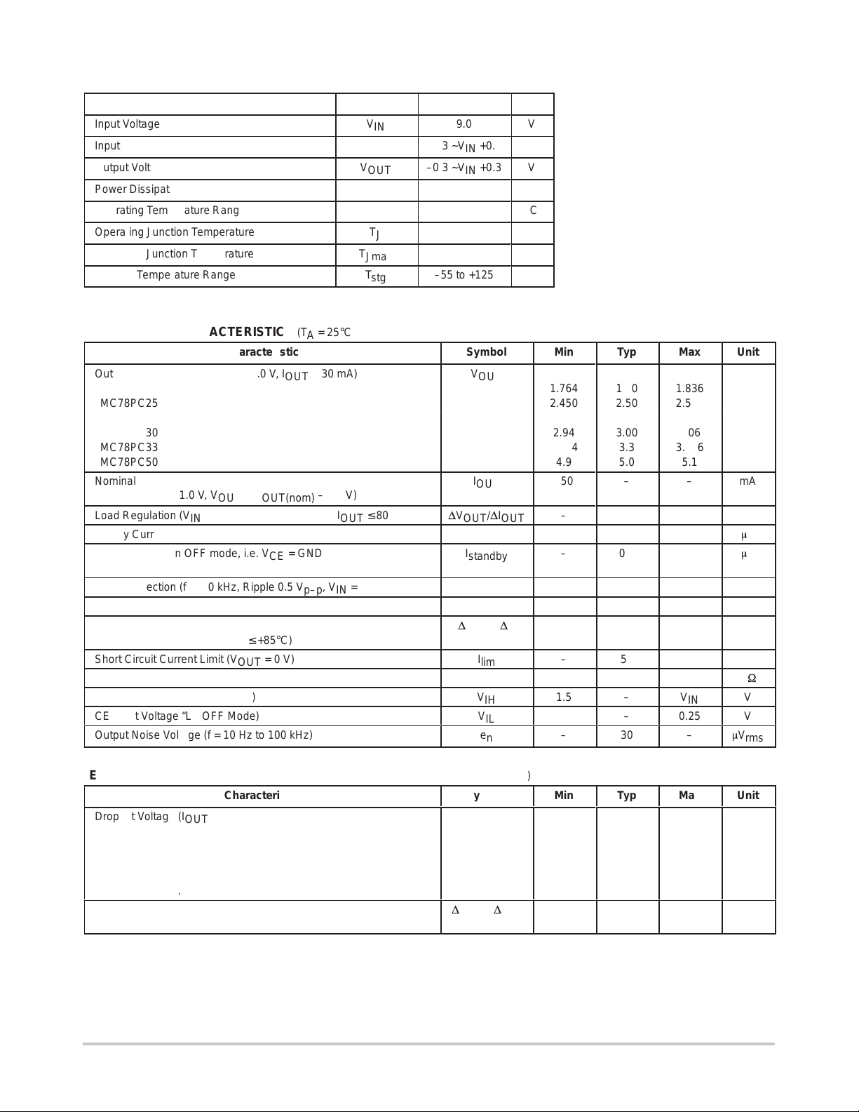
The MC78PC00 are a series of CMOS linear voltage regulators with
high output voltage accuracy, low supply current, low dropout voltage,
and high Ripple Rejection. Each of these voltage regulators consists of
an internal voltage reference, an error amplifier, resistors, a current
limiting circuit and a chip enable circuit.
The dynamic Response to line and load is fast, which makes these
products ideally suited for use in hand–held communication
equipment.
The MC78PC00 series are housed in the SOT–23 5 lead package,
for maximum board space saving.
MC78PC00 Features:
• Ultra–Low Supply Current: typical 35
• Standby Mode: typical 0.1
m
A.
• Low Dropout Voltage: typical 0.2 V @ I
• High Ripple Rejection: typical 70 dB @ f = 1 kHz.
• Low Temperature–Drift Coefficient of Output Voltage:
typical ±100 ppm/°C.
• Excellent Line Regulation: typical 0.05%/V.
• High Accuracy Output Voltage: ±2.0%.
• Fast Dynamic Response to Line and Load.
• Small Package: SOT–23 5 leads.
• Built–in Chip Enable circuit (CE input pin).
• Identical Pinout to the LP2980/1/2.
MC78PC00 Applications:
• Power source for cellular phones (GSM, CDMA, TDMA), Cordless
Phones (PHS, DECT) and 2–way radios.
• Power source for domestic appliances such as cameras, VCRs and
camcorders.
• Power source for battery–powered equipment.
Block Diagram
1
V
IN
m
A in ON mode with no load.
= 100 mA.
OUT
MC78PCxx
5
V
OUT
http://onsemi.com
5
1
SOT–23–5
N SUFFIX
CASE 1212
PIN CONNECTIONS
V
IN
GND
CE
DEVICE MARKING
(4 digits are available for device marking)
Marking Voltage Version
1 2
3 4
Pin # Symbol Description
1
2
3
4
5
K8
F5 2.5 V
F8 2.8 V
G0
G3
J0
PINS DESCRIPTION
V
IN
GND
CE
N/C
V
OUT
ORDERING INFORMATION
1
15
2
2
3
3
4
(Top View)
V
OUT
N/C
4
1.8 V
3.0 V
3.3 V
5.0 V
Lot Number
Input Pin
Ground Pin
Chip Enable Pin
No Connection
Output Pin
ref
CURRENT LIMIT
V
3
CE
Semiconductor Components Industries, LLC, 1999
October, 1999 – Rev. 2
Device ShippingPackage
MC78PC18NTR
MC78PC25NTR
MC78PC28NTR
MC78PC30NTR
MC78PC33NTR
2
GND
1 Publication Order Number:
MC78PC50NTR
Other voltages are available. Consult your ON Semiconductor
representative.
SOT–23
5 Leads
3000 Units
Tape & Reel
MC78PC00/D
MAXIMUM RATINGS
Á
Á
Á
Á
Á
Á
Rating Symbol Value Unit
Input Voltage
Input Voltage
Output Voltage
Power Dissipation
Operating Temperature Range
Operating Junction Temperature
Maximum Junction Temperature
Storage Temperature Range
MC78PC00 Series
V
V
V
T
Jmax
T
IN
CE
OUT
P
D
T
A
T
J
stg
9.0
–0.3 ~VIN +0.3
–0.3 ~VIN +0.3
250
–40 to +85
+125
+150
–55 to +125
V
V
V
mW
°C
°C
°C
°C
ELECTRICAL CHARACTERISTICS (T
Characteristic
Output Voltage (VIN = V
OUT
+ 1.0 V, I
OUT
= 25°C)
A
= 30 mA)
Symbol Min Typ Max Unit
V
OUT
MC78PC18 1.764 1.80 1.836
MC78PC25 2.450 2.50 2.550
MC78PC28 2.744 2.80 2.856
MC78PC30 2.94 3.00 3.06
MC78PC33 3.234 3.3 3.366
MC78PC50 4.9 5.0 5.1
Nominal Output Current
ББББББББББББББББ
(VIN = V
Load Regulation (VIN = V
Supply Current in ON mode (VIN = V
OUT
+ 1.0 V, V
= V
OUT
OUT(nom)
+ 1.0 V, 1.0 mA ≤ I
OUT
OUT
– 0.1 V)
+ 1.0 V, I
≤ 80 mA)
OUT
= 0 mA) I
OUT
Supply Current in OFF mode, i.e. VCE = GND I
(VIN = V
Ripple Rejection (f = 1.0 kHz, Ripple 0.5 V
OUT
+ 1.0 V, I
OUT
= 0 mA)
p–p
, VIN = V
+ 1.0 V) RR – 70 – dB
OUT
Input Voltage V
Output Voltage Temperature Coefficient
(I
= 30 mA, –40°C ≤ TA ≤ +85°C)
OUT
Short Circuit Current Limit (V
= 0 V) I
OUT
CE Pull–down Resistance R
CE Input Voltage “H” (ON Mode) V
CE Input Voltage “L” (OFF Mode) V
Output Noise Voltage (f = 10 Hz to 100 kHz)
I
OUT
ÁÁÁ
D
V
/DI
OUT
SS
standby
IN
D
V
OUT
lim
PD
IH
IL
e
n
OUT
/DT
150
ÁÁ
–
–
ÁÁ
12
– 35 70
– 0.1 1.0
– – 8.0 V
– ±100 – ppm/°C
– 50 – mA
2.5 5.0 10
1.5 – V
0 – 0.25 V
–
30
–
ÁÁ
40
IN
–
mA
Á
mV
m
m
M
m
V
V
A
A
W
V
rms
ELECTRICAL CHARACTERISTICS by OUTPUT VOLTAGE V
Characteristic
Dropout Voltage (I
1.8 ≤ V
OUT
2.0 ≤ V
OUT
2.5 ≤ V
OUT
2.8 ≤ V
OUT
3.4 ≤ V
OUT
Line Regulation
(V
+ 0.5 V ≤ VIN ≤ 8.0 V, I
OUT
≤ 1.9 – 0.60 1.40
≤ 2.4 – 0.35 0.70
≤ 2.7 – 0.24 0.35
≤ 3.3 – 0.20 0.30
≤ 6.0 – 0.17 0.26
OUT
= 100 mA)
OUT
= 30 mA) – 0.05 0.20
(T
OUT
Symbol Min Typ Max Unit
D
V
OUT
http://onsemi.com
2
A
V
DIF
= 25°C)
/DV
IN
V
%/V
MC78PC00 Series
OPERATION
MC78PC00
R1
R2
5
V
OUT
2
GND
1
V
IN
3
CE
In the MC78PC00, the output voltage V
ERROR AMP.
V
OUT
CURRENT LIMIT
ref
is detected by R1, R2. The detected output voltage is then compared to the
internal voltage reference by the error amplifier. Both a current limiting circuit for short circuit protection, and a chip ena ble
circuit are included.
http://onsemi.com
3
MC78PC00 Series
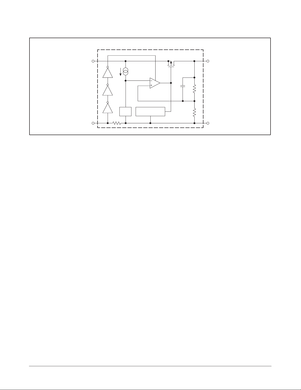
TEST CIRCUITS
Figure 1. Standard T est Circuits
3
CE
IN
0.1 mF
1
V
IN
MC78PCxx
Series
2 GND
Figure 3. Ripple Rejection, Line
Transient Response Test Circuit
3
CE
IN
P.G.
1
V
IN
MC78PCxx
Series
2 GND
5
V
5
V
OUT
OUT
I
OUT
2.2 mF
I
OUT
10 mF
OUT
OUT
IN
Figure 2. Supply Current Test Circuit
3
CE
IN
I
SS
0.1 mF
1
V
IN
MC78PCxx
Series
2 GND
Figure 4. Load Transient Response
T est Circuit
3
CE
1
MC78PCxx
Series
2 GND
V
1 mF
V
IN
5
OUT
5
V
OUT
10 mF
OUT
I
OUT
2.2 mF
I1 I2
OUT
http://onsemi.com
4
MC78PC00 Series
V
,
OUT
UT
VO
T
GE
(VO
T
)
IN
V
,
OUT
UT
VO
T
GE
(VO
T
)
IN
V,
OUT
UT
VO
T
GE
(VO
T
)
S
L
A
L
P
OUT
S
L
A
L
P
OUT
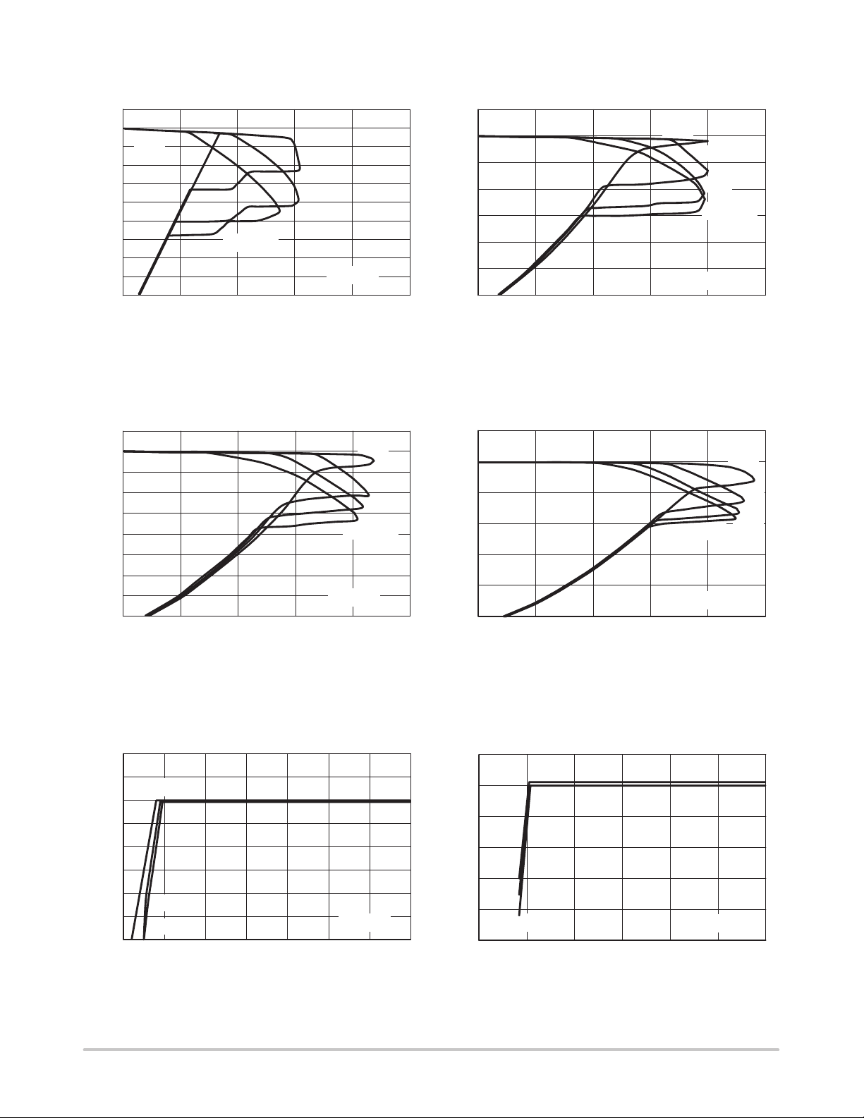
Figure 5. MC78PC18 Output Voltage versus
Output Current
2.0
1.8
3.8 V
1.6
1.4
1.2
1.0
0.8
0.6
0.4
0.2
VIN = 2.1 V
0
0
100 200 300 400 500
I
, OUTPUT CURRENT (mA)
OUT
2.8 V
2.3 V
Figure 7. MC78PC40 (4.0 V) Output Voltage
versus Output Current
4.5
4.0
3.5
3.0
2.5
2.0
1.5
1.0
0.5
0
0
100 200 300 400 500
I
, OUTPUT CURRENT (mA)
OUT
TA = 25°C
6.0 V
VIN = 4.3 V
TA = 25°C
5.0 V
4.5 V
, OUTPUT VOLTAGE (VOLTS)
OUT
V
, OUTPUT VOLTAGE (VOLTS)
OUT
V
Figure 6. MC78PC30 Output Voltage versus
Output Current
3.5
3.0
2.5
2.0
1.5
1.0
0.5
0
0
100 200 300 400 500
I
, OUTPUT CURRENT (mA)
OUT
5.0 V
Figure 8. MC78PC50 Output Voltage versus
Output Current
6.0
5.0
4.0
3.0
2.0
1.0
0
0
100 200 300 400 500
I
, OUTPUT CURRENT (mA)
OUT
VIN = 5.3 V
4.0 V
3.5 V
VIN = 3.3 V
TA = 25°C
7.0 V
6.0 V
5.5 V
TA = 25°C
S
L
A
L
P
OUT
Figure 9. MC78PC18 Output Voltage versus
Input Voltage
2.0
1.9
I
= 1 mA
OUT
1.8
1.7
1.6
1.5
1.4
1.3
1.2
1.0
30 mA
50 mA
2.0
3.0 4.0 5.0 6.0 7.0 8.0
V
, INPUT VOLTAGE (VOLTS)
TA = 25°C
http://onsemi.com
Figure 10. MC78PC30 Output Voltage versus
Input Voltage
3.1
3.0
2.9
2.8
1.0 mA
2.7
30 mA
2.6
OUT
V , OUTPUT VOLTAGE (VOLTS)
5
2.5
2.0
I
= 50 mA
OUT
3.0 4.0 5.0 6.0 7.0 8.0
V
, INPUT VOLTAGE (VOLTS)
TA = 25°C
 Loading...