

Datasheet MC78L24ACPRP, MC78L24ABPRP, MC78L24ABP, MC78L18ACPRA, MC78L18ACPRM Datasheet (MOTOROLA)
...
Semiconductor Components Industries, LLC, 1999
October, 1999 – Rev. 0
1 Publication Order Number:
MC78L00A/D
MC78L00A Series
Three-Terminal Low Current
Positive Voltage Regulators
The MC78L00A Series of positive voltage regulators are
inexpensive, easy–to–use devices suitable for a multitude of
applications that require a regulated supply of up to 100 mA. Like
their higher powered MC7800 and MC78M00 Series cousins, these
regulators feature internal current limiting and thermal shutdown
making them remarkably rugged. No external components are
required with the MC78L00 devices in many applications.
These devices offer a substantial performance advantage over the
traditional zener diode–resistor combination, as output impedance
and quiescent current are substantially reduced.
• Wide Range of Available, Fixed Output Voltages
• Low Cost
• Internal Short Circuit Current Limiting
• Internal Thermal Overload Protection
• No External Components Required
• Complementary Negative Regulators Offered (MC79L00A Series)
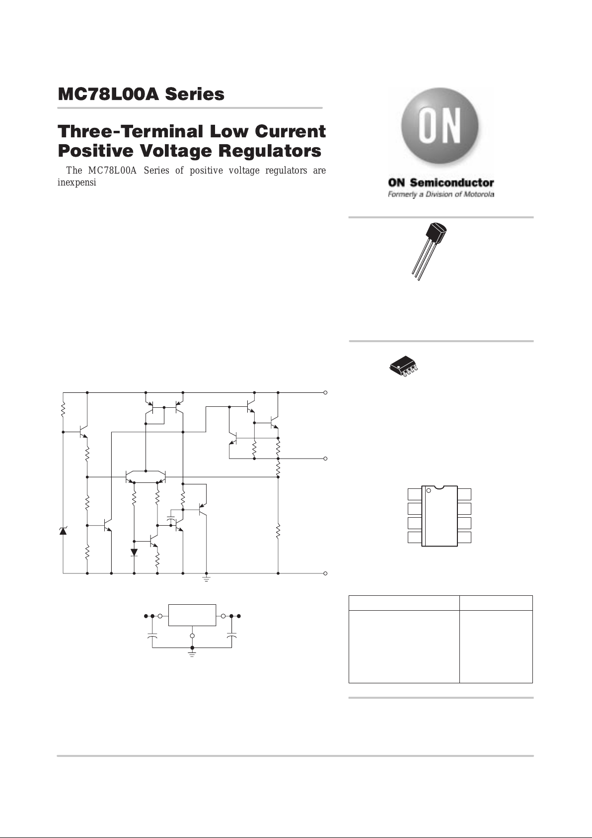
Representative Schematic Diagram
15k
Q1
Q3 Q5
Input
Output
Ground
Q11
Q12
3.0
0–25k
2.85k
5.0k
Q10
3.8k
Q4 Q6
1.2k
1.9k 19k 2.2k
Q9
Q8
C
Q7
1.0k
420
Z1
Q2
Standard Application
A common ground is required between the input and the output voltages. The
input voltage must remain typically 2.0 V above the output voltage even during
the low point on the input ripple voltage.
*Cin is required if regulator is located an *appreciable distance from power
supply filter.
**CO is not needed for stability; however, it does *improve transient response.
MC78LXXA
Input
Cin*
0.33µF
CO**
Output
TO–92
P SUFFIX
CASE 29
http://onsemi.com
See detailed ordering and shipping information in the package
dimensions section on page 7 of this data sheet.
ORDERING INFORMATION
2
3
1
Pin: 1. Output
2. Ground
3. Input
8
1
PIN CONNECTIONS
18
7
6
5
2
3
4
(Top View)
V
OUT
GND
GND
V
IN
GND
NC
GND
NC
SOP–8*
D SUFFIX
CASE 751
*SOP–8 is an internally modified SO–8 package. Pins
2, 3, 6, and 7 are electrically common to the die attach
flag. This internal lead frame modification decreases
package thermal resistance and increases power
dissipation capability when appropriately mounted on
a printed circuit board. SOP–8 conforms to all external dimensions of the standard SO–8 package.
DEVICE TYPE/NOMINAL VOLTAGE
5% Output Voltage Accuracy Voltage
MC78L05AC
MC78L08AC
MC78L09AC
MC78L12AC
MC78L15AC
MC78L18AC
MC78L24AC
5.0
8.0
9.0
12
15
18
24
MC78L00A Series
http://onsemi.com
2
MAXIMUM RATINGS (T
A
= +125°C, unless otherwise noted.)
Rating
Symbol Value Unit
Input Voltage (2.6 V–8.0 V)
Input Voltage (12 V–18 V)
Input Voltage (24 V)
V
I
30
35
40
Vdc
Storage Temperature Range T
stg
–65 to +150 °C
Operating Junction Temperature Range T
J
0 to +150 °C
ELECTRICAL CHARACTERISTICS (V
I
= 10 V, IO = 40 mA, CI = 0.33 µF, CO = 0.1 µF, – 40°C < TJ < +125°C (for MC78LXXAB),
0°C < TJ < +125°C (for MC78LXXAC), unless otherwise noted.)
MC78L05AC, AB
Characteristics Symbol Min Typ Max Unit
Output Voltage (TJ = +25°C) V
O
4.8 5.0 5.2 Vdc
Line Regulation
(TJ = +25°C, IO = 40 mA)
7.0 Vdc ≤ VI ≤ 20 Vdc
8.0 Vdc ≤ VI ≤ 20 Vdc
Reg
line
–
–
55
45
150
100
mV
Load Regulation
(TJ = +25°C, 1.0 mA ≤ IO ≤ 100 mA)
(TJ = +25°C, 1.0 mA ≤ IO ≤ 40 mA)
Reg
load
–
–
11
5.0
60
30
mV
Output Voltage
(7.0 Vdc ≤ VI ≤ 20 Vdc, 1.0 mA ≤ IO ≤ 40 mA)
(VI = 10 V, 1.0 mA ≤ IO ≤ 70 mA)
V
O
4.75
4.75
–
–
5.25
5.25
Vdc
Input Bias Current
(TJ = +25°C)
(TJ = +125°C)
I
IB
–
–
3.8
–
6.0
5.5
mA
Input Bias Current Change
(8.0 Vdc ≤ VI ≤ 20 Vdc)
(1.0 mA ≤ IO ≤ 40 mA)
∆I
IB
–
–
–
–
1.5
0.1
mA
Output Noise Voltage
(TA = +25°C, 10 Hz ≤ f ≤ 100 kHz)
V
n
– 40 – µV
Ripple Rejection (IO = 40 mA,
f = 120 Hz, 8.0 Vdc ≤ VI ≤ 18 V, TJ = +25°C)
RR 41 49 – dB
Dropout Voltage (TJ = +25°C) VI – V
O
– 1.7 – Vdc
MC78L00A Series
http://onsemi.com
3
ELECTRICAL CHARACTERISTICS (V
I
= 14 V, IO = 40 mA, CI = 0.33 µF, CO = 0.1 µF, – 40°C < TJ < +125°C (for MC78LXXAB),
0°C < TJ < +125°C (for MC78LXXAC), unless otherwise noted.)
MC78L08AC, AB
Characteristics Symbol Min Typ Max Unit
Output Voltage (TJ = +25°C) V
O
7.7 8.0 8.3 Vdc
Line Regulation
(TJ = +25°C, IO = 40 mA)
10.5 Vdc ≤ VI ≤ 23 Vdc
11 Vdc ≤ VI ≤ 23 Vdc
Reg
line
–
–
20
12
175
125
mV
Load Regulation
(TJ = +25°C, 1.0 mA ≤ IO ≤ 100 mA)
(TJ = +25°C, 1.0 mA ≤ IO ≤ 40 mA)
Reg
load
–
–
15
8.0
80
40
mV
Output Voltage
(10.5 Vdc ≤ VI ≤ 23 Vdc, 1.0 mA ≤ IO ≤ 40 mA)
(VI = 14 V, 1.0 mA ≤ IO ≤ 70 mA)
V
O
7.6
7.6
–
–
8.4
8.4
Vdc
Input Bias Current
(TJ = +25°C)
(TJ = +125°C)
I
IB
–
–
3.0
–
6.0
5.5
mA
Input Bias Current Change
(11 Vdc ≤ VI ≤ 23 Vdc)
(1.0 mA ≤ IO ≤ 40 mA)
∆I
IB
–
–
–
–
1.5
0.1
mA
Output Noise Voltage
(TA = +25°C, 10 Hz ≤ f ≤ 100 kHz)
V
n
– 60 – µV
Ripple Rejection (IO = 40 mA,
f = 120 Hz, 12 V ≤ VI ≤ 23 V, TJ = +25°C)
RR 37 57 – dB
Dropout Voltage (TJ = +25°C) VI – V
O
– 1.7 – Vdc
ELECTRICAL CHARACTERISTICS (V
I
= 15 V, IO = 40 mA, CI = 0.33 µF, CO = 0.1 µF, – 40°C < TJ < +125°C (for MC78LXXAB),
0°C < TJ < +125°C (for MC78LXXAC), unless otherwise noted.)
MC78L09AC, AB
Characteristics Symbol Min Typ Max Unit
Output Voltage (TJ = +25°C) V
O
8.6 9.0 9.4 Vdc
Line Regulation
(TJ = +25°C, IO = 40 mA)
11.5 Vdc ≤ VI ≤ 24 Vdc
12 Vdc ≤ VI ≤ 24 Vdc
Reg
line
–
–
20
12
175
125
mV
Load Regulation
(TJ = +25°C, 1.0 mA ≤ IO ≤ 100 mA)
(TJ = +25°C, 1.0 mA ≤ IO ≤ 40 mA)
Reg
load
–
–
15
8.0
90
40
mV
Output Voltage
(11.5 Vdc ≤ VI ≤ 24 Vdc, 1.0 mA ≤ IO ≤ 40 mA)
(VI = 15 V, 1.0 mA ≤ IO ≤ 70 mA)
V
O
8.5
8.5
–
–
9.5
9.5
Vdc
Input Bias Current
(TJ = +25°C)
(TJ = +125°C)
I
IB
–
–
3.0
–
6.0
5.5
mA
Input Bias Current Change
(11 Vdc ≤ VI ≤ 23 Vdc)
(1.0 mA ≤ IO ≤ 40 mA)
∆I
IB
–
–
–
–
1.5
0.1
mA
Output Noise Voltage
(TA = +25°C, 10 Hz ≤ f ≤ 100 kHz)
V
n
– 60 – µV
Ripple Rejection (IO = 40 mA,
f = 120 Hz, 13 V ≤ VI ≤ 24 V, TJ = +25°C)
RR 37 57 – dB
Dropout Voltage
(TJ = +25°C)
VI – V
O
– 1.7 – Vdc

MC78L00A Series
http://onsemi.com
4
ELECTRICAL CHARACTERISTICS (V
I
= 19 V, IO = 40 mA, CI = 0.33 µF, CO = 0.1 µF, – 40°C < TJ < +125°C (for MC78LXXAB),
0°C < TJ < +125°C (for MC78LXXAC), unless otherwise noted.)
MC78L12AC, AB
Characteristics Symbol Min Typ Max Unit
Output Voltage (TJ = +25°C) V
O
11.5 12 12.5 Vdc
Line Regulation
(TJ = +25°C, IO = 40 mA)
14.5 Vdc ≤ VI ≤ 27 Vdc
16 Vdc ≤ VI ≤ 27 Vdc
Reg
line
–
–
120
100
250
200
mV
Load Regulation
(TJ = +25°C, 1.0 mA ≤ IO ≤ 100 mA)
(TJ = +25°C, 1.0 mA ≤ IO ≤ 40 mA)
Reg
load
–
–
20
10
100
50
mV
Output Voltage
(14.5 Vdc ≤ VI ≤ 27 Vdc, 1.0 mA ≤ IO ≤ 40 mA)
(VI = 19 V, 1.0 mA ≤ IO ≤ 70 mA)
V
O
11.4
11.4
–
–
12.6
12.6
Vdc
Input Bias Current
(TJ = +25°C)
(TJ = +125°C)
I
IB
–
–
4.2
–
6.5
6.0
mA
Input Bias Current Change
(16 Vdc ≤ VI ≤ 27 Vdc)
(1.0 mA ≤ IO ≤ 40 mA)
∆I
IB
–
–
–
–
1.5
0.1
mA
Output Noise Voltage
(TA = +25°C, 10 Hz ≤ f ≤ 100 kHz)
V
n
– 80 – µV
Ripple Rejection (IO = 40 mA,
f = 120 Hz, 15 V ≤ VI ≤ 25 V, TJ = +25°C)
RR 37 42 – dB
Dropout Voltage
(TJ = +25°C)
VI – V
O
– 1.7 – Vdc
ELECTRICAL CHARACTERISTICS (V
I
= 23 V, IO = 40 mA, CI = 0.33 µF, CO = 0.1 µF, – 40°C < TJ < +125°C (for MC78LXXAB),
S 0°C < T
J
< +125°C (for MC78LXXAC), unless otherwise noted.)
MC78L15AC, AB
Characteristics Symbol Min Typ Max Unit
Output Voltage (TJ = +25°C) V
O
14.4 15 15.6 Vdc
Line Regulation
(TJ = +25°C, IO = 40 mA)
17.5 Vdc ≤ VI ≤ 30 Vdc
20 Vdc ≤ VI ≤ 30 Vdc
Reg
line
–
–
130
110
300
250
mV
Load Regulation
(TJ = +25°C, 1.0 mA ≤ IO ≤ 100 mA)
(TJ = +25°C, 1.0 mA ≤ IO ≤ 40 mA)
Reg
load
–
–
25
12
150
75
mV
Output Voltage
(17.5 Vdc ≤ VI ≤ 30 Vdc, 1.0 mA ≤ IO ≤ 40 mA)
(VI = 23 V, 1.0 mA ≤ IO ≤ 70 mA)
V
O
14.25
14.25
–
–
15.75
15.75
Vdc
Input Bias Current
(TJ = +25°C)
(TJ = +125°C)
I
IB
–
–
4.4
–
6.5
6.0
mA
Input Bias Current Change
(20 Vdc ≤ VI ≤ 30 Vdc)
(1.0 mA ≤ IO ≤ 40 mA)
∆I
IB
–
–
–
–
1.5
0.1
mA
Output Noise Voltage
(TA = +25°C, 10 Hz ≤ f ≤ 100 kHz)
V
n
– 90 – µV
Ripple Rejection (IO = 40 mA,
f = 120 Hz, 18.5 V ≤ VI ≤ 28.5 V, TJ = +25°C)
RR 34 39 – dB
Dropout Voltage
(TJ = +25°C)
VI – V
O
– 1.7 – Vdc

MC78L00A Series
http://onsemi.com
5
ELECTRICAL CHARACTERISTICS (V
I
= 27 V , IO = 40 mA, CI = 0.33 µF, CO = 0.1 µF, 0°C < TJ < +125°C, unless otherwise noted.)
MC78L18AC
Characteristics Symbol Min Typ Max Unit
Output Voltage (TJ = +25°C) V
O
17.3 18 18.7 Vdc
Line Regulation
(TJ = +25°C, IO = 40 mA)
21.4 Vdc ≤ VI ≤ 33 Vdc
20.7 Vdc ≤ VI ≤ 33 Vdc
22 Vdc ≤ VI ≤ 33 Vdc
21 Vdc ≤ VI ≤ 33 Vdc
Reg
line
–
–
45
35
325
275
mV
Load Regulation
(TJ = +25°C, 1.0 mA ≤ IO ≤ 100 mA)
(TJ = +25°C, 1.0 mA ≤ IO ≤ 40 mA)
Reg
load
–
–
30
15
170
85
mV
Output Voltage
(21.4 Vdc ≤ VI ≤ 33 Vdc, 1.0 mA ≤ IO ≤ 40 mA)
(20.7 Vdc ≤ VI ≤ 33 Vdc, 1.0 mA ≤ IO ≤ 40 mA)
(VI = 27 V, 1.0 mA ≤ IO ≤ 70 mA)
(VI = 27 V, 1.0 mA ≤ IO ≤ 70 mA)
V
O
17.1
17.1
–
–
18.9
18.9
Vdc
Input Bias Current
(TJ = +25°C)
(TJ = +125°C)
I
IB
–
–
3.1
–
6.5
6.0
mA
Input Bias Current Change
(22 Vdc ≤ VI ≤ 33 Vdc)
(21 Vdc ≤ VI ≤ 33 Vdc)
(1.0 mA ≤ IO ≤ 40 mA)
∆I
IB
–
–
–
–
1.5
0.1
mA
Output Noise Voltage
(TA = +25°C, 10 Hz ≤ f ≤ 100 kHz)
V
n
– 150 – µV
Ripple Rejection (IO = 40 mA,
f = 120 Hz, 23 V ≤ VI ≤ 33 V, TJ = +25°C)
RR 33 48 – dB
Dropout Voltage
(TJ = +25°C)
VI – V
O
– 1.7 – Vdc
ELECTRICAL CHARACTERISTICS (V
I
= 33 V , IO = 40 mA, CI = 0.33 µF, CO = 0.1 µF, 0°C < TJ < +125°C, unless otherwise noted.)
MC78L24AC
Characteristics Symbol Min Typ Max Unit
Output Voltage (TJ = +25°C) V
O
23 24 25 Vdc
Line Regulation
(TJ = +25°C, IO = 40 mA)
27.5 Vdc ≤ VI ≤ 38 Vdc
28 Vdc ≤ VI ≤ 80 Vdc
27 Vdc ≤ VI ≤ 38 Vdc
Reg
line
–
–
–
–
50
60
–
300
350
mV
Load Regulation
(TJ = +25°C, 1.0 mA ≤ IO ≤ 100 mA)
(TJ = +25°C, 1.0 mA ≤ IO ≤ 40 mA)
Reg
load
–
–
40
20
200
100
mV
Output Voltage
(28 Vdc ≤ VI ≤ 38 Vdc, 1.0 mA ≤ IO ≤ 40 mA)
(27 Vdc ≤ VI ≤ 38 Vdc, 1.0 mA ≤ IO ≤ 40 mA)
(28 Vdc ≤ VI = 33 Vdc, 1.0 mA ≤ IO ≤ 70 mA)
(27 Vdc ≤ VI ≤ 33 Vdc, 1.0 mA ≤ IO ≤ 70 mA)
V
O
22.8
22.8
–
–
25.2
25.2
Vdc
Input Bias Current
(TJ = +25°C)
(TJ = +125°C)
I
IB
–
–
3.1
–
6.5
6.0
mA
Input Bias Current Change
(28 Vdc ≤ VI ≤ 38 Vdc)
(1.0 mA ≤ IO ≤ 40 mA)
∆I
IB
–
–
–
–
1.5
0.1
mA
Output Noise Voltage
(TA = +25°C, 10 Hz ≤ f ≤ 100 kHz)
V
n
– 200 – µV
Ripple Rejection (IO = 40 mA,
f = 120 Hz, 29 V ≤ VI ≤ 35 V, TJ = +25°C)
RR 31 45 – dB
Dropout Voltage
(TJ = +25°C)
VI – V
O
– 1.7 – Vdc

MC78L00A Series
http://onsemi.com
6
P
D
, POWER DISSIPATION (mW)
I
IB
, INPUT BIAS CURRENT (mA)
I
IB
, INPUT BIAS CURRENT (mA) V
O
, OUTPUT VOLTAGE (V)
Figure 1. Dropout Characteristics
Figure 2. Dropout Voltage versus
Junction Temperature
Figure 3. Input Bias Current versus
Ambient Temperature
Figure 4. Input Bias Current
versus Input Voltage
Figure 5. Maximum Average Power Dissipation versus
Ambient Temperature – TO–92 Type Package
VI, INPUT VOLTAGE (V)
0 2.0 4.0 6.0 8.0 10
, INPUT/OUTPUT DIFFERENTIAL VOL TAGE (V)
IO
TJ, JUNCTION TEMPERATURE (°C)
0 25 50 75 100 125
–VV
Dropout of Regulation is
defined as when
VO = 2% of V
O
TA, AMBIENT TEMPERATURE (°C)
0 25 50 75 100 125
VI, INPUT VOLTAGE (V)
0 5.0 10 15 20 25 30 35 40
TA, AMBIENT TEMPERATURE (°C)
25 50 75 100 125 150
No Heatsink
8.0
6.0
4.0
2.0
0
2.5
2.0
1.5
1.0
0.5
0
4.2
4.0
3.8
3.6
3.4
3.2
3.0
0
5.0
4.0
3.0
2.0
1.0
0
10,000
1000
100
10
MC78L05AC
V
out
= 5.0 V
TJ = 25°C
MC78L05AC
V
out
= 5.0 V
IO = 40 mA
TJ = 25°C
R
θJA
= 200°C/W
P
D(max)
to 25°C = 625 mW
IO = 1.0 mA
IO = 40 mA
IO = 100 mA
IO = 70 mA
IO = 1.0 mA
IO = 40 mA
MC78L05AC
VI = 10 V
VO= 5.0 V
IO = 40 mA
30
50
70
90
110
130
150
0.4
0.8
1.2
1.6
2.0
2.4
2.8
02030504010
L, LENGTH OF COPPER (mm)
170
3.2
R
θJA
P
D
R , THERMAL RESISTANCE
JAθ
JUNCTION-TO-AIR ( C/W)°
, MAXIMUM POWER DISSIPATION (W)
2.0 oz.
Copper
Graph represents symmetrical layout
3.0 mmL
L
Figure 6. SOP–8 Thermal Resistance and Maximum
Power Dissipation versus P.C.B. Copper Length
P
D(max)
for TA = 50°C

MC78L00A Series
http://onsemi.com
7
APPLICATIONS INFORMATION
Design Considerations
The MC78L00A Series of fixed voltage regulators are
designed with Thermal Overload Protection that shuts
down the circuit when subjected to an excessive power
overload condition. Internal Short Circuit Protection limits
the maximum current the circuit will pass.
In many low current applications, compensation
capacitors are not required. However, it is recommended
that the regulator input be bypassed with a capacitor if the
regulator is connected to the power supply filter with long
wire lengths, or if the output load capacitance is large. The
input bypass capacitor should be selected to provide good
high–frequency characteristics to insure stable operation
under all load conditions. A 0.33 µF or larger tantalum,
mylar, or other capacitor having low internal impedance at
high frequencies should be chosen.The bypass capacitor
should be mounted with the shortest possible leads directly
across the regulators input terminals. Good construction
techniques should be used to minimize ground loops and
lead resistance drops since the regulator has no external
sense lead. Bypassing the output is also recommended.
Figure 7. Current Regulator Figure 8. ± 15 V Tracking Voltage Regulator
Figure 9. Positive and Negative Regulator
The MC78L00 regulators can also be used as a current source
when connected as above. In order to minimize dissipation the
MC78L05C is chosen in this application. Resistor R determines
the current as follows:
For example, a 100 mA current source would require R to be a
50 Ω, 1/2 W resistor and the output voltage compliance would be
the input voltage less 7 V.
IO =
5.0 V
+ I
B
IIB = 3.8 mA over line and load changes
Input
0.33µF
R
I
O
MC78L05A
Constant
Current to
Grounded Load
–
+
MC1741
+20V
0.33µF
MC78L15A +V
O
10k
10k
–V
O
7
6
2
3
4
6.5
20V
MPS A70
MPS U55
0.33µF
0.33µF
+V
I
–V
I
MC78LXXA
MC79LXXA
+V
O
–V
O
0.33µF
0.1µF
0.1µF
R
ORDERING INFORMATION
Device
Operating
Temperature Range
Package Shipping
MC78LXXACD* SOP–8 98 Units / Rail
MC78LXXACDR2* SOP–8 / Tape & Reel 2500 Units / Tape & Reel
MC78LXXACP
TJ = 0° to +125°C
TO–92 2000 Units / Bag
MC78LXXACPRA / MC78LXXACPRE TO–92 / Tape & Reel 2000 Units / Tape & Reel
MC78LXXACPRM / MC78LXXACPRP TO–92 / Ammo Pack 2000 Units / Ammo Pack
MC78LXXABD* SOP–8 98 Units / Rail
MC78LXXABDR2* SOP–8 / Tape & Reel 2500 Units / Tape & Reel
MC78LXXABP*
TJ = –40° to +125°C
TO–92 2000 Units / Bag
MC78LXXABPRA / MC78LXXABPRE TO–92 / Tape & Reel 2000 Units / Tape & Reel
MC78LXXABPRM / MC78LXXABPRP TO–92 / Ammo Pack 2000 Units / Ammo Pack
XX indicates nominal voltage
*Available in 5, 8, 9, 12 and 15 V devices.

MC78L00A Series
http://onsemi.com
8
P ACKAGE DIMENSIONS
P SUFFIX
PLASTIC PACKAGE
CASE 29–04
ISSUE AD
R
A
P
J
L
F
B
K
G
H
SECTION X–X
C
V
D
N
N
XX
SEATING
PLANE
1
NOTES:
1. DIMENSIONING AND TOLERANCING PER ANSI
Y14.5M, 1982.
2. CONTROLLING DIMENSION: INCH.
3. CONTOUR OF PACKAGE BEYOND DIMENSION R
IS UNCONTROLLED.
4. DIMENSION F APPLIES BETWEEN P AND L.
DIMENSION D AND J APPLY BETWEEN L AND K
MINIMUM. LEAD DIMENSION IS UNCONTROLLED
IN P AND BEYOND DIMENSION K MINIMUM.
DIM MIN MAX MIN MAX
MILLIMETERSINCHES
A 0.175 0.205 4.45 5.20
B 0.170 0.210 4.32 5.33
C 0.125 0.165 3.18 4.19
D 0.016 0.022 0.41 0.55
F 0.016 0.019 0.41 0.48
G 0.045 0.055 1.15 1.39
H 0.095 0.105 2.42 2.66
J 0.015 0.020 0.39 0.50
K 0.500 ––– 12.70 –––
L 0.250 ––– 6.35 –––
N 0.080 0.105 2.04 2.66
P ––– 0.100 ––– 2.54
R 0.115 ––– 2.93 –––
V 0.135 ––– 3.43 –––
(SOP–8)
D SUFFIX
PLASTIC PACKAGE
CASE 751–05
ISSUE R
SEATING
PLANE
1
4
58
A0.25MCB
SS
0.25MB
M
h
q
C
X 45
_
L
DIM MIN MAX
MILLIMETERS
A 1.35 1.75
A1 0.10 0.25
B 0.35 0.49
C 0.18 0.25
D 4.80 5.00
E
1.27 BSCe
3.80 4.00
H 5.80 6.20
h
0 7
L 0.40 1.25
q
0.25 0.50
__
NOTES:
1. DIMENSIONING AND TOLERANCING PER ASME
Y14.5M, 1994.
2. DIMENSIONS ARE IN MILLIMETERS.
3. DIMENSION D AND E DO NOT INCLUDE MOLD
PROTRUSION.
4. MAXIMUM MOLD PROTRUSION 0.15 PER SIDE.
5. DIMENSION B DOES NOT INCLUDE MOLD
PROTRUSION. ALLOWABLE DAMBAR
PROTRUSION SHALL BE 0.127 TOTAL IN EXCESS
OF THE B DIMENSION AT MAXIMUM MATERIAL
CONDITION.
D
E
H
A
B
e
B
A1
C
A
0.10
USA/EUROPE Literature Fulfillment:
Literature Distribution Center for ON Semiconductor
P.O. Box 5163, Denver, Colorado 80217 USA
Phone: 303–675–2175 or 800–344–3860 T oll Free USA/Canada
Fax: 303–675–2176 or 800–344–3867 Toll Free USA/Canada
Email: ONlit@hibbertco.com
Fax Response Line*: 303–675–2167
800–344–3810 Toll Free USA/Canada
*To receive a Fax of our publications
N. America Technical Support: 800–282–9855 Toll Free USA/Canada
ON Semiconductor and are trademarks of Semiconductor Components Industries, LLC (SCILLC). SCILLC reserves the right to make changes
without further notice to any products herein. SCILLC makes no warranty , representation or guarantee regarding the suitability of its products for any particular
purpose, nor does SCILLC assume any liability arising out of the application or use of any product or circuit, and specifically disclaims any and all liability ,
including without limitation special, consequential or incidental damages. “Typical” parameters which may be provided in SCILLC data sheets and/or
specifications can and do vary in different applications and actual performance may vary over time. All operating parameters, including “Typicals” must be
validated for each customer application by customer’s technical experts. SCILLC does not convey any license under its patent rights nor the rights of others.
SCILLC products are not designed, intended, or authorized for use as components in systems intended for surgical implant into the body, or other applications
intended to support or sustain life, or for any other application in which the failure of the SCILLC product could create a situation where personal injury or death
may occur. Should Buyer purchase or use SCILLC products for any such unintended or unauthorized application, Buyer shall indemnify and hold SCILLC
and its officers, employees, subsidiaries, affiliates, and distributors harmless against all claims, costs, damages, and expenses, and reasonable attorney fees
arising out of, directly or indirectly, any claim of personal injury or death associated with such unintended or unauthorized use, even if such claim alleges that
SCILLC was negligent regarding the design or manufacture of the part. SCILLC is an Equal Opportunity/Affirmative Action Employer.
PUBLICATION ORDERING INFORMATION
ASIA/PACIFIC: LDC for ON Semiconductor – Asia Support
Phone: 303–675–2121 (Tue–Fri 9:00am to 1:00pm, Hong Kong T ime)
Email: ONlit–asia@hibbertco.com
JAPAN: ON Semiconductor, Japan Customer Focus Center
4–32–1 Nishi–Gotanda, Shinagawa–ku, T okyo, Japan 141–8549
Phone: 81–3–5487–8345
Email: r14153@onsemi.com
ON Semiconductor Website: http://onsemi.com
For additional information, please contact your local Sales Representative.
MC78L00A/D
 Loading...