

Motorola MC74LVQ04D, MC74LVQ04DT, MC74LVQ04M, MC74LVQ04SD Datasheet
SEMICONDUCTOR TECHNICAL DATA
Motorola, Inc. 1995
1
11/95
REV 1
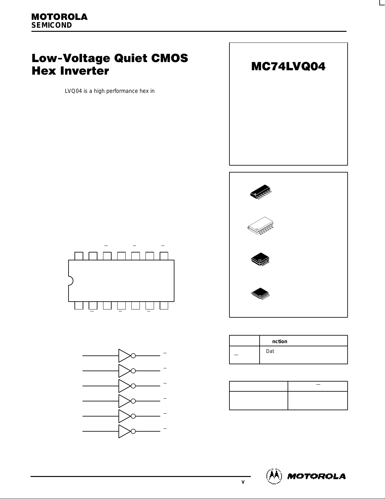
The MC74LVQ04 is a high performance hex inverter operating from a
2.7 to 3.6V supply. High impedance TTL compatible inputs significantly
reduce current loading to input drivers while TTL compatible outputs offer
improved switching noise performance.
Current drive capability is 12mA at the outputs.
• Designed for 2.7 to 3.6V V
CC
Operation – Ideal for Low Power/Low
Noise Applications
• Guaranteed Simultaneous Switching Noise Level and Dynamic
Threshold Performance
• Guaranteed Skew Specifications
• Guaranteed Incident Wave Switching into 75Ω
• Low Static Supply Current (10µA) Substantially Reduces System Power
Requirements
• Latchup Performance Exceeds 500mA
• ESD Performance: Human Body Model >2000V
Pinout: 14–Lead (Top View)
1314 12 11 10 9 8
21 3 4 5 6 7
V
CC
A3 O
3 A4 O4 A5 O5
A0 O
0 A1 O1 A2 O2 GND
2
O
0
1
A0
LOGIC DIAGRAM
4
O
1
3
A1
6
O
2
5
A2
12
O
3
13
A3
10
O
4
11
A4
8
O
5
9
A5
LOW–VOLTAGE CMOS
HEX INVERTER
LVQ
PIN NAMES
Function
Data Inputs
Outputs
Pins
An
O
n
FUNCTION TABLE
An On
L
H
H
L
DT SUFFIX
PLASTIC TSSOP
CASE 948G–01
14
1
SD SUFFIX
PLASTIC SSOP
CASE 940A–03
14
1
M SUFFIX
PLASTIC SOIC EIAJ
CASE 965–01
14
1
D SUFFIX
PLASTIC SOIC
CASE 751A–03
14
1
MC74LVQ04
MOTOROLA LVQ DATA
BR1478
2
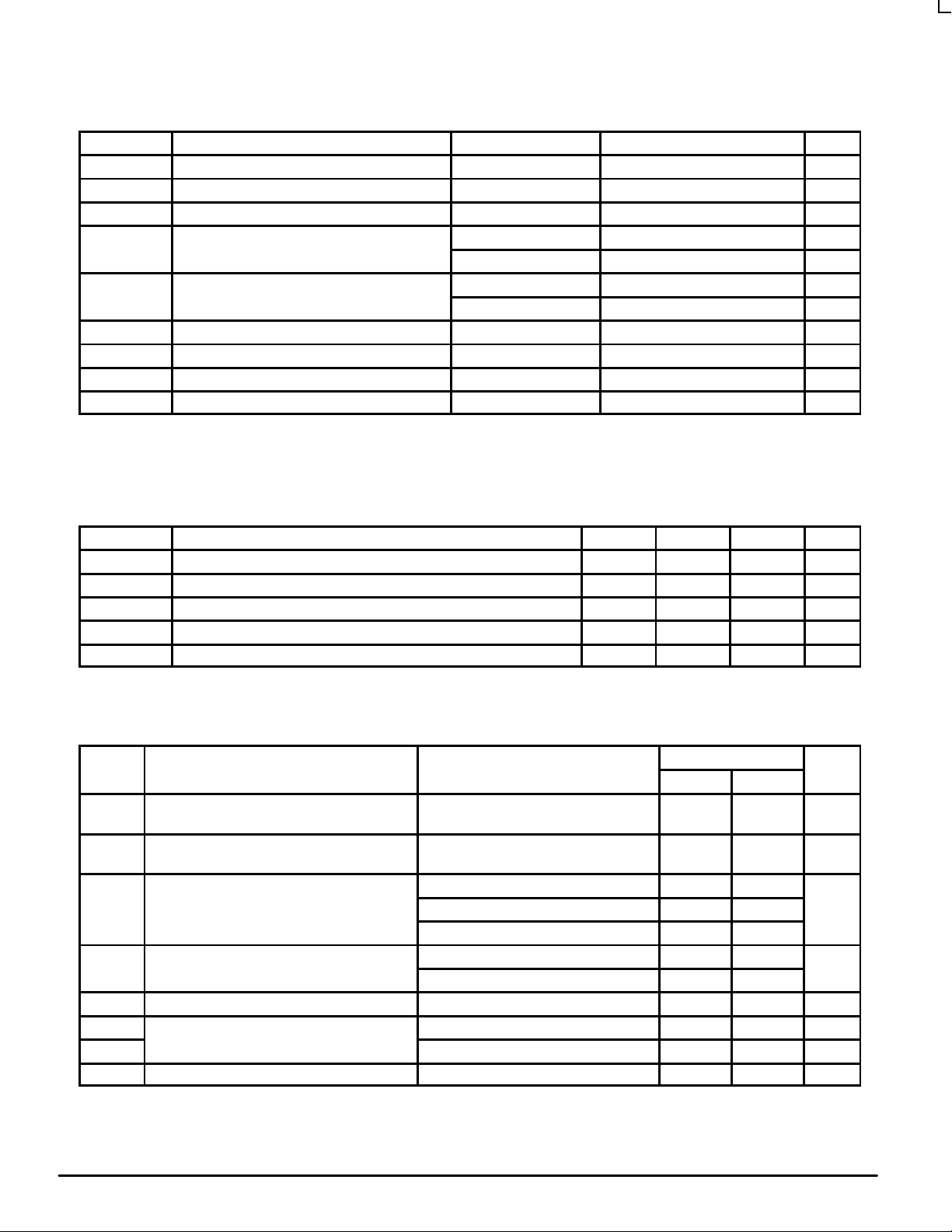
ABSOLUTE MAXIMUM RATINGS*
Symbol Parameter Value Condition Unit
V
CC
DC Supply Voltage –0.5 to +7.0 V
V
I
DC Input Voltage –0.5 ≤ VI ≤ VCC + 0.5V V
V
O
DC Output Voltage –0.5 ≤ VO ≤ VCC + 0.5 Output in HIGH or LOW State V
I
IK
DC Input Diode Current –20 VI = –0.5V mA
+20 VI = VCC + 0.5V mA
I
OK
DC Output Diode Current –20 VO = –0.5V mA
+20 VI = VCC + 0.5V mA
I
O
DC Output Source/Sink Current ±50 mA
I
CC
DC Supply Current ±200 mA
I
GND
DC Ground Current ±200 mA
T
STG
Storage Temperature Range –65 to +150 °C
* Absolute maximum continuous ratings are those values beyond which damage to the device may occur. Exposure to these conditions or
conditions beyond those indicated may adversely affect device reliability. Functional operation under absolute–maximum–rated conditions is
not implied.
RECOMMENDED OPERATING CONDITIONS
Symbol Parameter Min Typ Max Unit
V
CC
Supply Voltage 2.0 3.3 3.6 V
V
I
Input Voltage 0 V
CC
V
V
O
Output Voltage 0 V
CC
V
T
A
Operating Free–Air Temperature –40 +85 °C
∆V/∆t Input Transition Rise or Fall Rate, VIN from 0.8V to 2.0V, VCC = 3.0V 0 125 mV/ns
DC ELECTRICAL CHARACTERISTICS
TA = –40°C to +85°C
Symbol Characteristic Condition Min Max Unit
V
IH
HIGH Level Input Voltage (Note 1) 2.7V ≤ VCC ≤ 3.6V,
VO = 0.1V or VCC – 0.1V
2.0 V
V
IL
LOW Level Input Voltage (Note 1) 2.7V ≤ VCC ≤ 3.6V,
VO = 0.1V or VCC – 0.1V
0.8 V
V
OH
HIGH Level Output Voltage 2.7V ≤ VCC ≤ 3.6V; IOH = –50µA VCC– 0.1 V
VCC = 2.7V; IOH = –12mA 2.2
VCC = 3.0V; IOH = –12mA 2.48
V
OL
LOW Level Output Voltage 2.7V ≤ VCC ≤ 3.6V; IOL = 50µA 0.1 V
2.7V ≤ VCC ≤ 3.6V; IOL= 12mA 0.4
I
I
Input Leakage Current 2.7V ≤ VCC ≤3.6V; VI= VCC, GND ±1.0 µA
I
OLD
Minimum Dynamic Output Current (Note 2) VCC = 3.6V; V
OLD
= 0.8V Max 36 mA
I
OHD
VCC = 3.6V; V
OHD
= 2.0V Min –25 mA
I
CC
Quiescent Supply Current 2.7V ≤ VCC ≤3.6V; VI = VCC, GND 10 µA
1. These values of VI are used to test DC electrical characteristics only. Functional test should use VIH ≥ 2.4V, VIL ≤ 0.5V.
2. Incident wave switching on transmission lines with impedances as low as 75Ω for commercial temperature range is guaranteed. Maximum test
duration is 2ms, one output loaded at a time.
MC74LVQ04
LCX DATA
BR1478
3 MOTOROLA
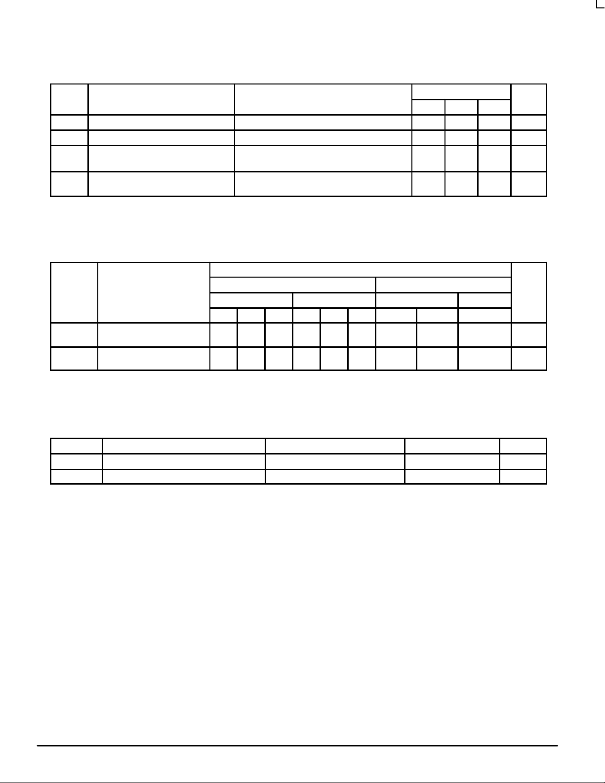
DYNAMIC SWITCHING CHARACTERISTICS (VCC = 3.3V)
TA = +25°C
Symbol Characteristic Condition Min Typ Max Unit
V
OLP
Dynamic LOW Peak Voltage (Note 1) CL = 50pF, VIH = 3.3V, VIL = 0V 0.6 1.0 V
V
OLV
Dynamic LOW Valley Voltage (Note 1) CL = 50pF, VIH = 3.3V, VIL = 0V –0.5 –1.0 V
V
IHD
High Level Dynamic Input Voltage
(Note 2)
Input–Under–Test Switching 0V to Threshold,
f=1MHz
1.5 2.0 V
V
ILD
Low Level Dynamic Input Voltage
(Note 2)
Input–Under–Test Switching 3.3V to Threshold,
f=1MHz
1.5 0.8 V
1. Number of outputs defined as “n”. Measured with “n–1” outputs switching from HIGH–to–LOW. The remaining output is measured in the LOW
state.
2. Number of data inputs is defined as “n” switching, “n–1” inputs switching 0V to 3.3V.
AC CHARACTERISTICS (tR = tF = 2.5ns; CL = 50pF; RL = 500Ω)
Limits
TA = +25°C TA = –40°C to +85°C
VCC = 3.0V to 3.6V VCC = 2.7V VCC = 3.0V to 3.6V VCC = 2.7V
Symbol Parameter Min Typ Max Min Typ Max Min Max Max Unit
t
PLH
t
PHL
Propagation Delay Input to
Output
1.5
1.5
5.0
5.0
9.0
8.5
1.5
1.5
6.5
5.4
10.5
9.5
1.0
1.0
10.0
9.5
11.0
10.0
ns
t
OSHL
t
OSLH
Output–to–Output Skew
(Note 1)
1.0
1.0
1.5
1.5
1.0
1.0
1.5
1.5
1.5
1.5
ns
1. Skew is defined as the absolute value of the difference between the actual propagation delay for any two separate outputs of the same device.
The specification applies to any outputs switching in the same direction, either HIGH–to–LOW (t
OSHL
) or LOW–to–HIGH (t
OSLH
); parameter
guaranteed by design.
CAPACITIVE CHARACTERISTICS
Symbol Parameter Condition Typical Unit
C
PD
Power Dissipation Capacitance 10MHz, VCC = 3.3V, VI = 0V or V
CC
14 pF
C
IN
Input Capacitance VCC = Open, VI = 0V or V
CC
4.5 pF
 Loading...