

Motorola MC74LCX74M, MC74LCX74DT, MC74LCX74D, MC74LCX74SD Datasheet
SEMICONDUCTOR TECHNICAL DATA
!
"
The MC74LCX74 is a high performance, dual D–type flip–flop with
asynchronous clear and set inputs and complementary (O, O
operates from a 2.7 to 3.6V supply. High impedance TTL compatible
inputs significantly reduce current loading to input drivers while TTL
compatible outputs offer improved switching noise performance. A V
specification of 5.5V allows MC74LCX74 inputs to be safely driven from
5V devices.
The MC74LCX74 consists of 2 edge–triggered flip–flops with
individual D–type inputs. The flip–flop will store the state of individual D
inputs, that meet the setup and hold time requirements, on the
LOW–to–HIGH Clock (CP) transition.
) outputs. It
I
LOW–VOLTAGE CMOS
DUAL D–TYPE FLIP–FLOP
• Designed for 2.7 to 3.6V V
Operation
CC
• 5V Tolerant Inputs — Interface Capability With 5V TTL Logic
• LVTTL Compatible
• LVCMOS Compatible
• 24mA Balanced Output Sink and Source Capability
• Near Zero Static Supply Current in All Three Logic States (10µA)
Substantially Reduces System Power Requirements
• Latchup Performance Exceeds 500mA
• ESD Performance: Human Body Model >2000V; Machine Model >200V
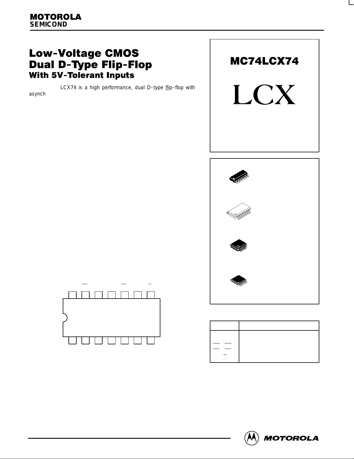
Pinout: 14–Lead (Top View)
VCCCD
CD
2 D2 CP2 SD2O2 O2
1314 12 11 10 9 8
21 34567
1 D1 CP1 SD1O1 O1 GND
14
14
14
14
PIN NAMES
Pins
CP1, CP2
D1, D2
CD
1, CD2
SD1, SD2
On, O
n
1
1
1
1
Function
Clock Pulse Inputs
Data Inputs
Direct Clear Inputs
Direct Set Inputs
Outputs
D SUFFIX
PLASTIC SOIC
CASE 751A–03
M SUFFIX
PLASTIC SOIC EIAJ
CASE 965–01
SD SUFFIX
PLASTIC SSOP
CASE 940A–03
DT SUFFIX
PLASTIC TSSOP
CASE 948G–01
11/96
Motorola, Inc. 1996
1
REV 1
MC74LCX74
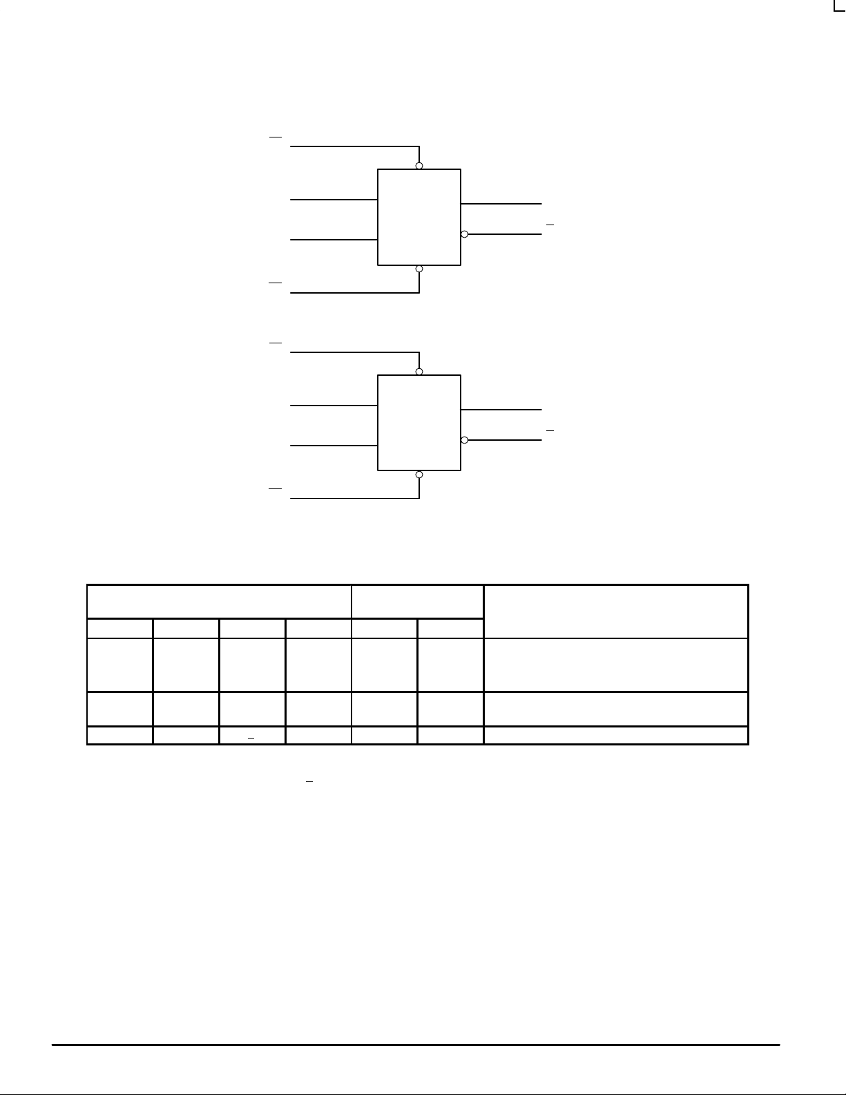
LOGIC DIAGRAM
SD1
CP1 CP
CD1
SD2
CP2 CP
CD2
4
2
D1 D
3
1
10
12
D2 D
11
13
SD
CD
SD
CD
5
Q
Q
Q
Q
O1
6
O
1
9
O2
8
O
2
INPUTS OUTPUTS
SDn CDn CPn Dn On On
L
H
L L X X H H Undetermined
H
H
H H ↑ X NC NC Hold
H = High Voltage Level; h = High V oltage Level One Setup T ime Prior to the Low–to–High Clock Transition; L = Low Voltage Level; l = Low
Voltage Level One Setup T ime Prior to the Low–to–High Clock T ransition; NC = No Change; X = High or Low Voltage Level or Transitions
are Acceptable; ↑ = Low–to–High T ransition; ↑
H
L
H
H
X
X
↑
↑
X
X
h
l
= Not a Low–to–High Transition; For ICC Reasons DO NOT FLOAT Inputs
H
L
H
L
L
H
L
H
OPERATING MODE
Asynchronous Set
Asynchronous Clear
Load and Read Register
MOTOROLA LCX DATA
2
BR1339 — REV 3
MC74LCX74
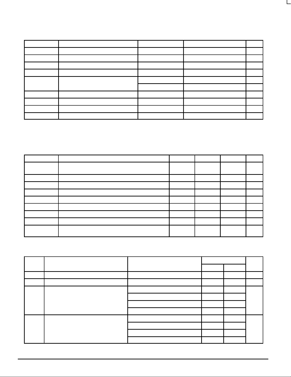
ABSOLUTE MAXIMUM RATINGS*
Symbol Parameter Value Condition Unit
V
CC
V
I
V
O
I
IK
I
OK
I
O
I
CC
I
GND
T
STG
* Absolute maximum continuous ratings are those values beyond which damage to the device may occur. Exposure to these conditions or
conditions beyond those indicated may adversely affect device reliability. Functional operation under absolute–maximum–rated conditions is
not implied.
1. Output in HIGH or LOW State. IO absolute maximum rating must be observed.
RECOMMENDED OPERATING CONDITIONS
Symbol Parameter Min Typ Max Unit
V
CC
V
I
V
O
I
OH
I
OL
I
OH
I
OL
T
A
∆t/∆V Input Transition Rise or Fall Rate, VIN from 0.8V to 2.0V ,
DC Supply Voltage –0.5 to +7.0 V
DC Input Voltage –0.5 ≤ VI ≤ +7.0 V
DC Output Voltage –0.5 ≤ VO ≤ VCC + 0.5 Note 1. V
DC Input Diode Current –50 VI < GND mA
DC Output Diode Current –50 VO < GND mA
+50 VO > V
DC Output Source/Sink Current ±50 mA
DC Supply Current Per Supply Pin ±100 mA
DC Ground Current Per Ground Pin ±100 mA
Storage Temperature Range –65 to +150 °C
Supply Voltage Operating
Data Retention Only
Input Voltage 0 5.5 V
Output Voltage (HIGH or LOW State) 0 V
HIGH Level Output Current, VCC = 3.0V – 3.6V –24 mA
LOW Level Output Current, VCC = 3.0V – 3.6V 24 mA
HIGH Level Output Current, VCC = 2.7V – 3.0V –12 mA
LOW Level Output Current, VCC = 2.7V – 3.0V 12 mA
Operating Free–Air Temperature –40 +85 °C
VCC = 3.0V
2.0
1.5
0 10 ns/V
3.3
3.3
CC
3.6
3.6
CC
mA
V
V
DC ELECTRICAL CHARACTERISTICS
TA = –40°C to +85°C
Symbol Characteristic Condition Min Max Unit
V
IH
V
IL
V
OH
V
OL
2. These values of VI are used to test DC electrical characteristics only.
LCX DATA
BR1339 — REV 3
HIGH Level Input Voltage (Note 2.) 2.7V ≤ VCC ≤ 3.6V 2.0 V
LOW Level Input Voltage (Note 2.) 2.7V ≤ VCC ≤ 3.6V 0.8 V
HIGH Level Output Voltage 2.7V ≤ VCC ≤ 3.6V; IOH = –100µA VCC– 0.2 V
VCC = 2.7V; IOH = –12mA 2.2
VCC = 3.0V; IOH = –18mA 2.4
VCC = 3.0V; IOH = –24mA 2.2
LOW Level Output Voltage 2.7V ≤ VCC ≤ 3.6V; IOL = 100µA 0.2 V
VCC = 2.7V; IOL= 12mA 0.4
VCC = 3.0V; IOL = 16mA 0.4
VCC = 3.0V; IOL = 24mA 0.55
3 MOTOROLA
 Loading...