

Motorola MC74LCX652DW, MC74LCX652SD, MC74LCX652DT Datasheet
SEMICONDUCTOR TECHNICAL DATA
&-&$*! *$
(%) #, ( !#)* (
(%) #, ( #*" +$ %$
#*" &$ (%* %'+*) % +*'+*)
** &%%, (*#%!
The MC74LCX652 is a high performance, non–inverting octal
transceiver/registered transceiver operating from a 2.7 to 3.6V supply.
High impedance TTL compatible inputs significantly reduce current
loading to input drivers while TTL compatible outputs offer improved
switching noise performance. A VI specification of 5.5V allows
MC74LCX652 inputs to be safely driven from 5V devices. The
MC74LCX652 is suitable for memory address driving and all TTL level
bus oriented transceiver applications.
Data on the A or B bus will be clocked into the registers as the
appropriate clock pin goes from a LOW–to–HIGH logic level. Two Output
Enable pins (OEBA
outputs. In the transceiver mode, data present at the high impedance port
may be stored in either the A or the B register or in both. The select
controls (SBA, SAB) can multiplex stored and real–time (transparent
mode) data. In the isolation mode (both outputs disabled), A data may be
stored in the B register or B data may be stored in the A register. When in
the real–time mode, it is possible to store data without using the internal
registers by simultaneously enabling OEAB and OEBA
configuration, each output reinforces its input (data retention is not
guaranteed in this mode).
, OEAB) are provided to control the transceiver
. In this
LOW–VOLTAGE CMOS
OCTAL TRANSCEIVER/
REGISTERED TRANSCEIVER
WITH DUAL ENABLE
DW SUFFIX
24–LEAD PLASTIC SOIC PACKAGE
CASE 751E–04
• Designed for 2.7 to 3.6V V
Operation
CC
• 5V Tolerant — Interface Capability With 5V TTL Logic
• Supports Live Insertion and Withdrawal
• I
Specification Guarantees High Impedance When VCC = 0V
OFF
• LVTTL Compatible
• LVCMOS Compatible
• 24mA Balanced Output Sink and Source Capability
• Near Zero Static Supply Current in All Three Logic States (10µA)
Substantially Reduces System Power Requirements
• Latchup Performance Exceeds 500mA
• ESD Performance: Human Body Model >2000V; Machine Model >200V
V
CBA SBA OEBA B0 B1 B2 B3 B4 B5
CC
2324 22 21 20 19 18
21 34567
CAB SAB OEAB A0 A1 A2 A3 A4 A5 A6
17
16
9
8
15
10
B6 B7
14
13
11
12
A7 GND
24–LEAD PLASTIC SSOP PACKAGE
24–LEAD PLASTIC TSSOP PACKAGE
PIN NAMES
Pins
A0–A7
B0–B7
CAB, CBA
SAB, SBA
OEBA
, OEAB
SD SUFFIX
CASE 940D–03
DT SUFFIX
CASE 948H–01
Function
Side A Inputs/Outputs
Side B Inputs/Outputs
Clock Pulse Inputs
Select Control Inputs
Output Enable Inputs
3/97
Motorola, Inc. 1997
Figure 1. 24–Lead Pinout (Top View)
1
REV 1
MC74LCX652
O
1
CBA
3
OEAB
21
OEBA
22
SBA
2
SAB
23
CAB
A0
1 of 8 Channels
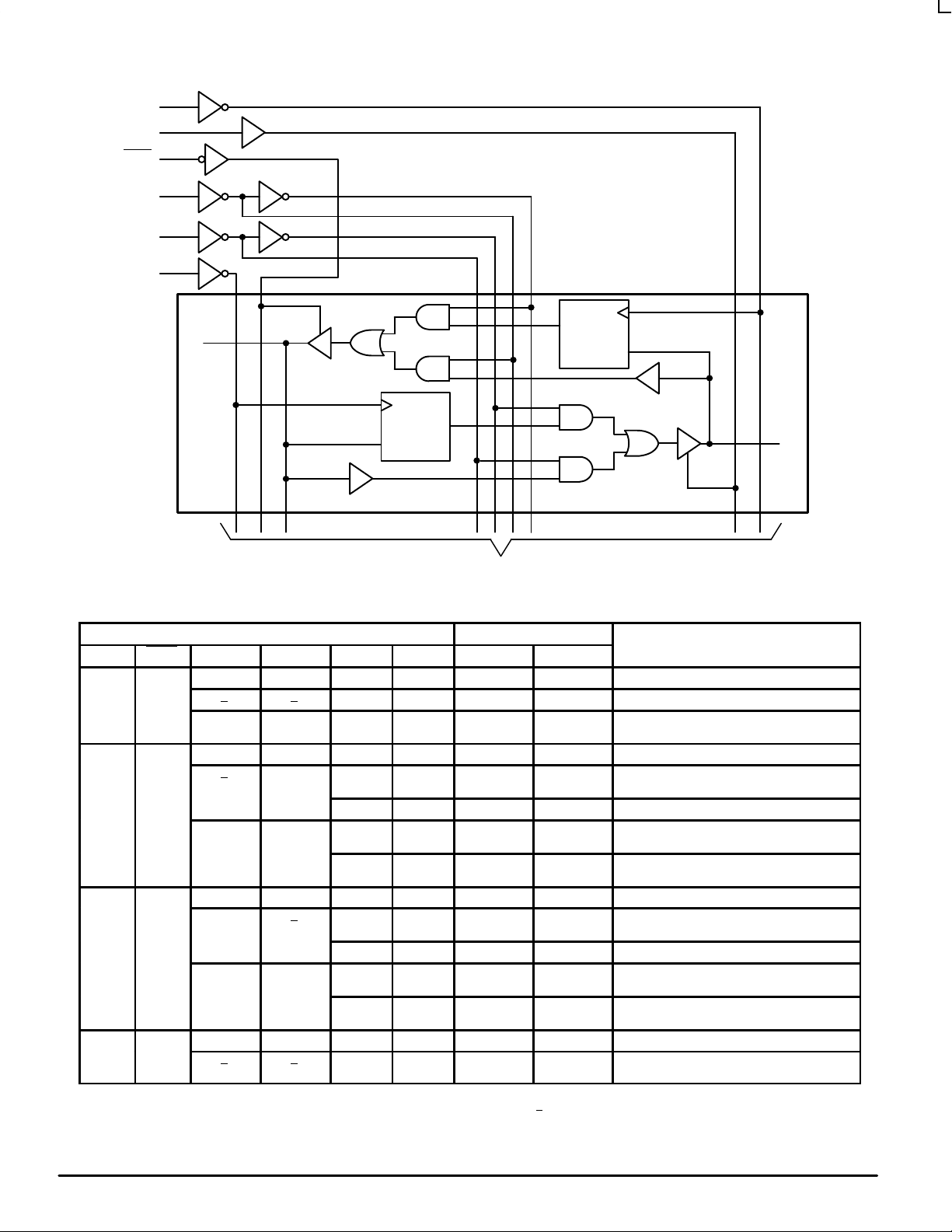
Figure 2. Logic Diagram
C
Q
D
C
Q
D
B0
To 7 Other Channels
FUNCTION TABLE
Inputs
OEAB OEBA CAB CBA SAB SBA An Bn
L H Input Input
↑ ↑ X X X X Isolation, Hold Storage
↑ ↑ X X l
H H Input Output
↑ X* L X L
H X X QA Stored A Data to B Bus
↑ X* L X l
H X L
L L Output Input
X* ↑ X L L
X H QB X Stored B Data to A Bus
X* ↑ X L L
X H QB
H L Output Output
↑ ↑ H H QB QA Stored A Data to B Bus,
H = High Voltage Level; h = High Voltage Level One Setup Time Prior to the Low–to–High Clock Transition; L = Low Voltage Level; l = Low Voltage Level One Setup
Time Prior to the Low–to–High Clock T ransition; X = Don’t Care; ↑ = Low–to–High Clock Transition; ↑
QB = B input storage register; * = The clocks are not internally gated with either the Output Enables or the Source Inputs. Therefore, data at the A or B ports may be
clocked into the storage registers, at any time. For ICC reasons, Do Not Float Inputs.
Data Ports
h
H
h
H
H
H
QB
perating Mode
l
h
L
H
L
H
QA
QA
L
H
l
h
L
H
= NOT Low–to–High Clock Transition; QA = A input storage register;
Store A and/or B Data
Real Time A Data to B Bus
Real Time A Data to B Bus; Store A Data
Clock A Data to B Bus; Store A Data
Real Time B Data to A Bus
Real Time B Data to A Bus; Store B Data
Clock B Data to A Bus; Store B Data
Stored B Data to A Bus
MOTOROLA LCX DATA
2
BR1339 — REV 3
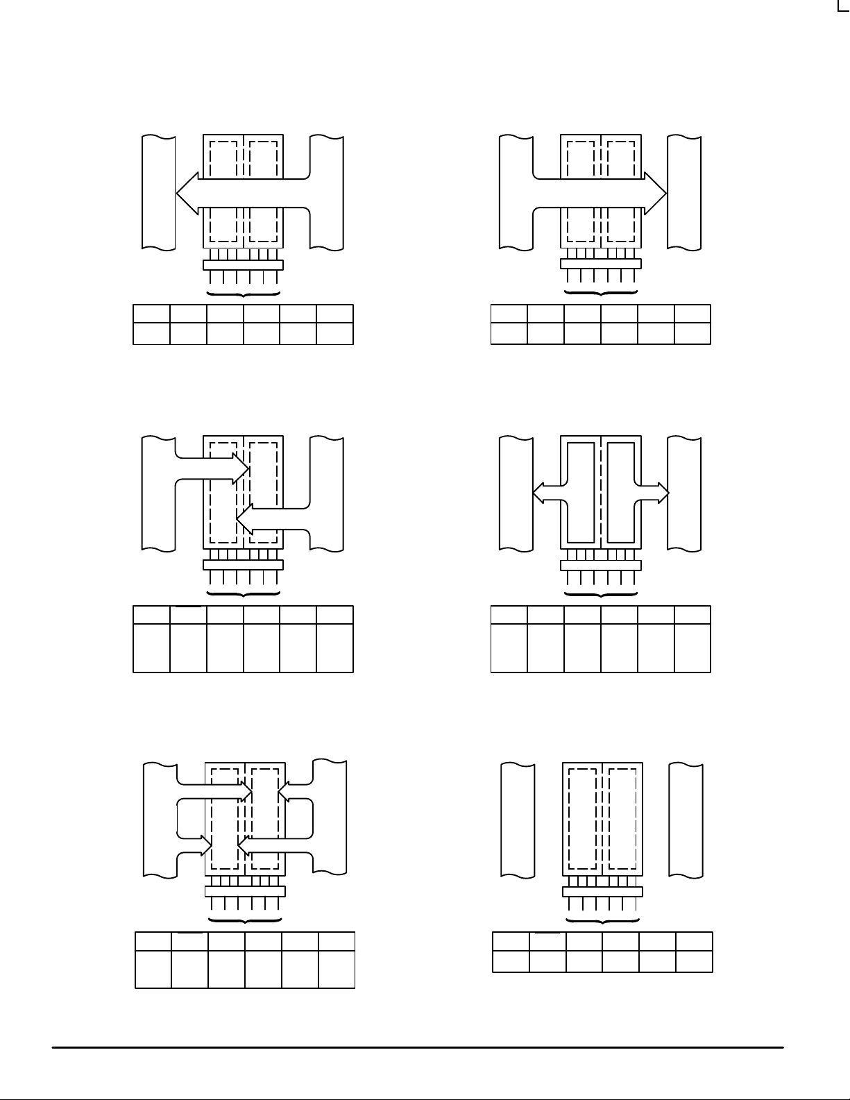
MC74LCX652
Real Time Transfer – Bus B to
Bus A
BUS A
OEABLOEBA
CABXCBAXSABXSBA
L
Store Data from Bus A, Bus B or
Bus A and Bus B
BUS B
L
Real Time Transfer – Bus A to
Bus B
BUS A
OEABHOEBA
CABXCBAXSABLSBA
H
Transfer A Stored Data to Bus B
or B Stored Data to Bus A or
Both at the Same Time
BUS B
X
BUS A
OEBA
H
X
H
CAB
↑
X
↑
CBA
X
↑
↑
SAB
X
X
X
OEAB
X
L
L
Store Bus A in Both Registers or
Store Bus B in Both Registers
BUS A
BUS B
SBA
X
X
X
BUS B
OEAB
H
L
H
BUS A
OEBA
H
L
L
BUS A
CAB
H or L
X
H or L
Isolation
CBA
X
H or L
H or L
SAB
H
X
H
BUS B
SBA
X
H
H
BUS B
OEAB
LCX DATA
BR1339 — REV 3
CAB
CBA
H or L
SABXSBA
X
CAB
OEBA
H
H
L
L
CBA
↑
↑
↑
↑
SAB
L
X
SBA
X
L
OEABLOEBA
H
H or L
Figure 3. Bus Applications
3 MOTOROLA
 Loading...