

MOTOROLA MC74LCX573DTR2, MC74LCX573ML2, MC74LCX573DWR2, MC74LCX573MEL, MC74LCX573DTEL Datasheet
SEMICONDUCTOR TECHNICAL DATA
1
REV 3
Motorola, Inc. 1996
11/96
")" & &
$!%#$!& &
") $"' !"'&
& " $!& !#'&% ! '&#'&%
&& "!!($&!
The MC74LCX573 is a high performance, non–inverting octal
transparent latch operating from a 2.7 to 3.6V supply. High impedance
TTL compatible inputs significantly reduce current loading to input drivers
while TTL compatible outputs offer improved switching noise
performance. A VI specification of 5.5V allows MC74LCX573 inputs to be
safely driven from 5V devices.
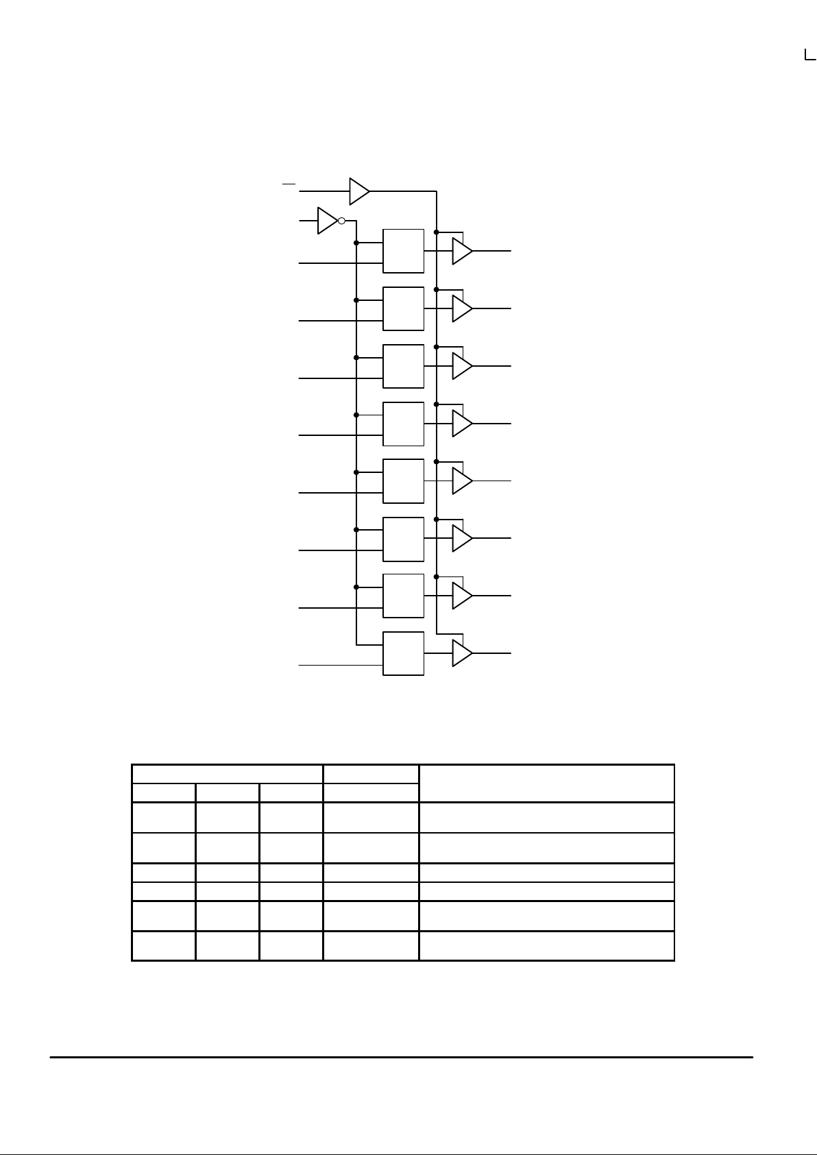
The MC74LCX573 contains 8 D–type latches with 3–state standard
outputs. When the Latch Enable (LE) input is HIGH, data on the Dn inputs
enters the latches. In this condition, the latches are transparent, i.e., a
latch output will change state each time its D input changes. When LE is
LOW, the latches store the information that was present on the D inputs a
setup time preceding the HIGH–to–LOW transition of LE. The 3–state
standard outputs are controlled by the Output Enable (OE
) input. When
OE
is LOW, the standard outputs are enabled. When OE is HIGH, the
standard outputs are in the high impedance state, but this does not
interfere with new data entering into the latches. The LCX573 flow
through design facilitates easy PC board layout.
• Designed for 2.7 to 3.6V V
CC
Operation
• 5V T olerant — Interface Capability With 5V TTL Logic
• Supports Live Insertion and Withdrawal
• I
OFF
Specification Guarantees High Impedance When VCC = 0V
• LVTTL Compatible
• LVCMOS Compatible
• 24mA Balanced Output Sink and Source Capability
• Near Zero Static Supply Current in All Three Logic States (10µA)
Substantially Reduces System Power Requirements
• Latchup Performance Exceeds 500mA
• ESD Performance: Human Body Model >2000V; Machine Model >200V
Pinout: 20–Lead (Top View)
1920 18 17 16 15 14
21 34567
V
CC
13
8
12
9
11
10
O0 O1 O2 O3 O4 O5 O6 O7 LE
OE
D0 D1 D2 D3 D4 D5 D6 D7 GND
DW SUFFIX
PLASTIC SOIC
CASE 751D–04
DT SUFFIX
PLASTIC TSSOP
CASE 948E–02
20
1
20
1
M SUFFIX
PLASTIC SOIC EIAJ
CASE 967–01
20
1
SD SUFFIX
PLASTIC SSOP
CASE 940C–03
20
1
PIN NAMES
Function
Output Enable Input
Latch Enable Input
Data Inputs
3–State Latch Outputs
Pins
OE
LE
D0–D7
O0–O7
LOW–VOL TAGE
CMOS OCTAL
TRANSPARENT LATCH
MC74LCX573
MOTOROLA LCX DATA
BR1339 — REV 3
2
O0
D0
O1
D1
O2
D2
O3
D3
O4
D4
O5
D5
O6
D6
O7
D7
LOGIC DIAGRAM
nLE
Q
D
nLE
Q
D
nLE
Q
D
nLE
Q
D
nLE
Q
D
nLE
Q
D
nLE
Q
D
nLE
Q
D
LE
OE
2
3
4
5
6
7
8
9
19
18
17
16
15
14
13
12
11
1
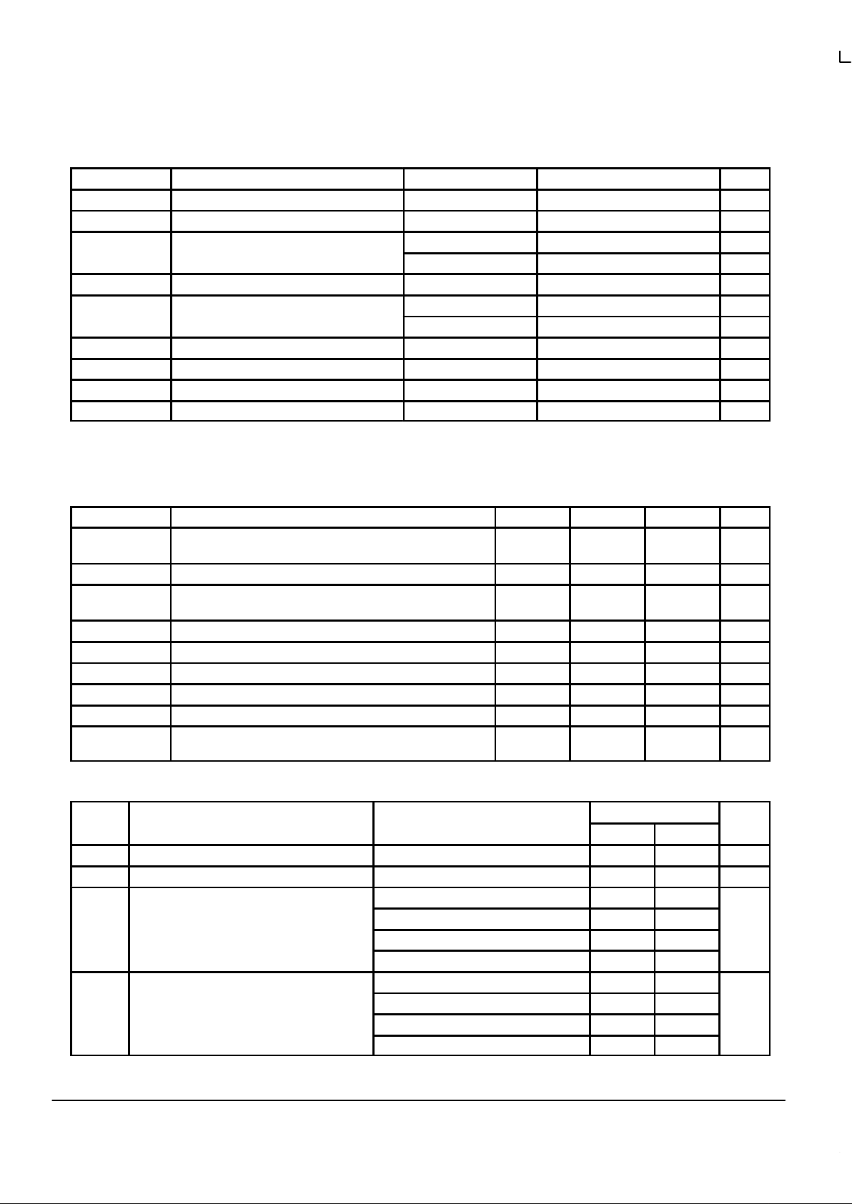
INPUTS OUTPUTS
OE LE Dn On OPERATING MODE
L
L
H
H
H
L
H
L
Transparent (Latch Disabled); Read Latch
L
L
L
L
h
l
H
L
Latched (Latch Enabled) Read Latch
L L X NC Hold; Read Latch
H L X Z Hold; Disabled Outputs
H
H
H
H
H
L
Z
Z
Transparent (Latch Disabled); Disabled Outputs
H
H
L
L
h
l
Z
Z
Latched (Latch Enabled); Disabled Outputs
H = High Voltage Level; h = High Voltage Level One Setup Time Prior to the Latch Enable High–to–Low Transition;
L = Low Voltage Level; l = Low Voltage Level One Setup Time Prior to the Latch Enable High–to–Low Transition;
NC = No Change, State Prior to the Latch Enable High–to–Low Transition; X = High or Low V oltage Level or Transitions
are Acceptable; Z = High Impedance State; For ICC Reasons DO NOT FLOAT Inputs
MC74LCX573
LCX DATA
BR1339 — REV 3
3 MOTOROLA
ABSOLUTE MAXIMUM RATINGS*
Symbol Parameter Value Condition Unit
V
CC
DC Supply Voltage –0.5 to +7.0 V
V
I
DC Input Voltage –0.5 ≤ VI ≤ +7.0 V
V
O
DC Output Voltage –0.5 ≤ VO ≤ +7.0 Output in 3–State V
–0.5 ≤ VO ≤ VCC + 0.5 Note 1. V
I
IK
DC Input Diode Current –50 VI < GND mA
I
OK
DC Output Diode Current –50 VO < GND mA
+50 VO > V
CC
mA
I
O
DC Output Source/Sink Current ±50 mA
I
CC
DC Supply Current Per Supply Pin ±100 mA
I
GND
DC Ground Current Per Ground Pin ±100 mA
T
STG
Storage Temperature Range –65 to +150 °C
* Absolute maximum continuous ratings are those values beyond which damage to the device may occur. Exposure to these conditions or conditions
beyond those indicated may adversely affect device reliability. Functional operation under absolute–maximum–rated conditions is not implied.
1. Output in HIGH or LOW State. IO absolute maximum rating must be observed.
RECOMMENDED OPERATING CONDITIONS
Symbol Parameter Min Typ Max Unit
V
CC
Supply Voltage Operating
Data Retention Only
2.0
1.5
3.3
3.3
3.6
3.6
V
V
I
Input Voltage 0 5.5 V
V
O
Output Voltage (HIGH or LOW State)
(3–State)
0
0
V
CC
5.5
V
I
OH
HIGH Level Output Current, VCC = 3.0V – 3.6V –24 mA
I
OL
LOW Level Output Current, VCC = 3.0V – 3.6V 24 mA
I
OH
HIGH Level Output Current, VCC = 2.7V – 3.0V –12 mA
I
OL
LOW Level Output Current, VCC = 2.7V – 3.0V 12 mA
T
A
Operating Free–Air Temperature –40 +85 °C
∆t/∆V Input Transition Rise or Fall Rate, VIN from 0.8V to 2.0V ,
VCC = 3.0V
0 10 ns/V
DC ELECTRICAL CHARACTERISTICS
TA = –40°C to +85°C
Symbol Characteristic Condition Min Max Unit
V
IH
HIGH Level Input Voltage (Note 2.) 2.7V ≤ VCC ≤ 3.6V 2.0 V
V
IL
LOW Level Input Voltage (Note 2.) 2.7V ≤ VCC ≤ 3.6V 0.8 V
V
OH
HIGH Level Output Voltage 2.7V ≤ VCC ≤ 3.6V; IOH = –100µA VCC– 0.2 V
VCC = 2.7V; IOH = –12mA 2.2
VCC = 3.0V; IOH = –18mA 2.4
VCC = 3.0V; IOH = –24mA 2.2
V
OL
LOW Level Output Voltage 2.7V ≤ VCC ≤ 3.6V; IOL = 100µA 0.2 V
VCC = 2.7V; IOL= 12mA 0.4
VCC = 3.0V; IOL = 16mA 0.4
VCC = 3.0V; IOL = 24mA 0.55
2. These values of VI are used to test DC electrical characteristics only.
 Loading...