

Motorola MC74LCX543DW, MC74LCX543SD, MC74LCX543DT Datasheet
SEMICONDUCTOR TECHNICAL DATA
' $ $
$ "#&"
$ "$ !%$# %$!%$#
$$ &"$
The MC74LCX543 is a high performance, non–inverting octal latching
transceiver operating from a 2.7 to 3.6V supply. High impedance TTL
compatible inputs significantly reduce current loading to input drivers
while TTL compatible outputs offer improved switching noise
performance. A VI specification of 5.5V allows MC74LCX543 inputs to be
safely driven from 5V devices. The MC74LCX543 is suitable for memory
address driving and all TTL level bus oriented transceiver applications.
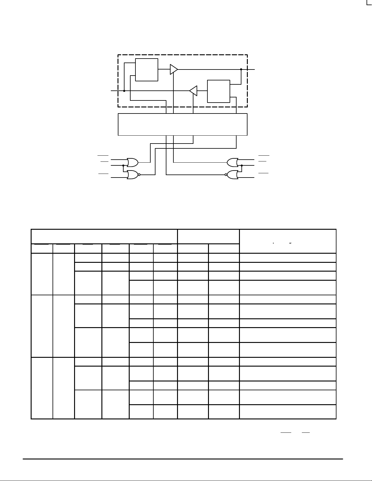
For data flow from A to B with the EAB
Enable (OEAB
indicated in the Function Table. With EAB
A–to–B Latch Enable (LEAB
transparent; a subsequent LOW–to–HIGH transition of the LEAB
will latch the A latches, and the outputs no longer change with the A
inputs. With EAB
active and reflect the data present at the output of the A latches. Control
of data flow from B to A is symetric to that above, but uses the EBA
LEBA
, and OEBA inputs.
• Designed for 2.7 to 3.6V V
) must be LOW in order to enable data to the B bus, as
) input makes the A–to–B latches
and OEAB both LOW, the 3–State B output buf fers are
Operation
CC
• 5V Tolerant — Interface Capability With 5V TTL Logic
• Supports Live Insertion and Withdrawal
• I
Specification Guarantees High Impedance When VCC = 0V
OFF
• LVTTL Compatible
• LVCMOS Compatible
• 24mA Balanced Output Sink and Source Capability
• Near Zero Static Supply Current in All Three Logic States (10µA)
Substantially Reduces System Power Requirements
• Latchup Performance Exceeds 500mA
• ESD Performance: Human Body Model >2000V; Machine Model >200V
LOW, the A–to–B Output
LOW, a LOW signal on the
signal
,
LOW–VOLTAGE CMOS
OCTAL LATCHING
TRANSCEIVER
DW SUFFIX
24
1
24
1
24
1
PLASTIC SOIC
CASE 751E–04
SD SUFFIX
PLASTIC SSOP
CASE 940D–03
DT SUFFIX
PLASTIC TSSOP
CASE 948H–01
Pinout: 24–Lead Package (Top View)
V
EBA
CC
LEBA
This document contains information on a new product. Specifications and information herein are subject to
change without notice.
11/96
Motorola, Inc. 1996
B0 B1 B2 B3 B4 B5 B6 B7
2324 22 21 20 19 18
21 34567
OEBA A0 A1 A2 A3 A4 A5 A6 A7
17
1
16
9
8
15
10
LEAB
OEAB
14
13
11
12
EAB GND
PIN NAMES
Pins
OExx
Exx
LExx
A0–A7
B0–B7
REV 0.3
Function
Output Enable Inputs
Enable Inputs
Latch Enable Inputs
3–State Inputs/Outputs
3–State Inputs/Outputs
MC74LCX543
Operating Mode
LOGIC DIAGRAM
D
Q
LE
3
A0
Q
DETAIL A x 7
OEBA
LEBA
2 13
EBA
23
1
FUNCTION TABLE
Inputs
OEAB OEBA EAB EBA LEAB LEBA An Bn
H H Input Input
X X X X X X Disable Outputs
L L L L X X Transparent Data; Outputs Disabled
H H l
L H Input Output
H X* L X l
H X X Z Hold; B Outputs Disabled
L X* L X L
H X l
H L Output Input
X* H X L Z
X H Z X Hold; A Outputs DIsabled
X* L X L L
X H L
Data
Ports
h
h
H
h
Z
H
H
DETAIL A
D
LE
l
h
Z
Z
L
H
L
H
l
h
L
H
l
h
22
B0
OEAB
EAB
11
LEAB
14
Operating Mode
Latch and Outputs Disabled
Load and B Outputs Disabled
Transparent A to B
Latch and Display B Outputs
Load and A Outputs Disabled
Transparent B to A
Latch and Display A Outputs
H = High Voltage Level; h = High Voltage Level One Setup T ime Prior to the Latch Enable or Enable Low–to–High Transition; L = Low Voltage Level;
l = Low Voltage Level One Setup Time Prior to the Latch Enable or Enable Low–to–High T ransition; X = Don’t Care; * = The latches are not internally
gated with the Output Enables. Therefore, data at the A or B ports may enter the latches at any time, provided that the LExx
and Exx pins are set
accordingly. For ICC reasons, Do Not Float Inputs.
MOTOROLA LCX DATA
2
BR1339 — REV 3
MC74LCX543
ABSOLUTE MAXIMUM RATINGS*
Symbol Parameter Value Condition Unit
V
CC
V
I
V
O
I
IK
I
OK
I
O
I
CC
I
GND
T
STG
* Absolute maximum continuous ratings are those values beyond which damage to the device may occur. Exposure to these conditions or conditions
beyond those indicated may adversely affect device reliability. Functional operation under absolute–maximum–rated conditions is not implied.
1. Output in HIGH or LOW State. IO absolute maximum rating must be observed.
RECOMMENDED OPERATING CONDITIONS
Symbol Parameter Min Typ Max Unit
V
CC
V
I
V
O
I
OH
I
OL
I
OH
I
OL
T
A
∆t/∆V Input Transition Rise or Fall Rate, VIN from 0.8V to 2.0V ,
DC Supply Voltage –0.5 to +7.0 V
DC Input Voltage –0.5 ≤ VI ≤ +7.0 V
DC Output Voltage –0.5 ≤ VO ≤ +7.0 Output in 3–State V
–0.5 ≤ VO ≤ VCC + 0.5 Note 1. V
DC Input Diode Current –50 VI < GND mA
DC Output Diode Current –50 VO < GND mA
+50 VO > V
DC Output Source/Sink Current ±50 mA
DC Supply Current Per Supply Pin ±100 mA
DC Ground Current Per Ground Pin ±100 mA
Storage Temperature Range –65 to +150 °C
Supply Voltage Operating
Data Retention Only
Input Voltage 0 5.5 V
Output Voltage (HIGH or LOW State)
(3–State)
HIGH Level Output Current, VCC = 3.0V – 3.6V –24 mA
LOW Level Output Current, VCC = 3.0V – 3.6V 24 mA
HIGH Level Output Current, VCC = 2.7V – 3.0V –12 mA
LOW Level Output Current, VCC = 2.7V – 3.0V 12 mA
Operating Free–Air Temperature –40 +85 °C
VCC = 3.0V
2.0
1.5
0
0
0 10 ns/V
3.3
3.3
CC
V
3.6
3.6
CC
5.5
mA
V
V
DC ELECTRICAL CHARACTERISTICS
TA = –40°C to +85°C
Symbol Characteristic Condition Min Max Unit
V
IH
V
IL
V
OH
V
OL
2. These values of VI are used to test DC electrical characteristics only.
LCX DATA
BR1339 — REV 3
HIGH Level Input Voltage (Note 2.) 2.7V ≤ VCC ≤ 3.6V 2.0 V
LOW Level Input Voltage (Note 2.) 2.7V ≤ VCC ≤ 3.6V 0.8 V
HIGH Level Output Voltage 2.7V ≤ VCC ≤ 3.6V; IOH = –100µA VCC– 0.2 V
VCC = 2.7V; IOH = –12mA 2.2
VCC = 3.0V; IOH = –18mA 2.4
VCC = 3.0V; IOH = –24mA 2.2
LOW Level Output Voltage 2.7V ≤ VCC ≤ 3.6V; IOL = 100µA 0.2 V
VCC = 2.7V; IOL= 12mA 0.4
VCC = 3.0V; IOL = 16mA 0.4
VCC = 3.0V; IOL = 24mA 0.55
3 MOTOROLA
 Loading...