

Motorola MC74LCX157SD, MC74LCX157DT, MC74LCX157D Datasheet
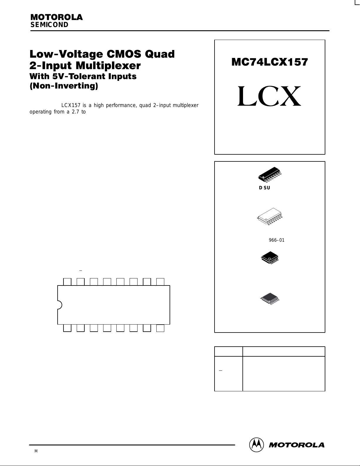
SEMICONDUCTOR TECHNICAL DATA
' $ %
!%$ %$!("
$ "$ !%$#
&"$
The MC74LCX157 is a high performance, quad 2–input multiplexer
operating from a 2.7 to 3.6V supply. High impedance TTL compatible
inputs significantly reduce current loading to input drivers while TTL
compatible outputs offer improved switching noise performance. A V
specification of 5.5V allows MC74LCX157 inputs to be safely driven from
5V devices.
Four bits of data from two sources can be selected using the Select
and Enable inputs. The four outputs present the selected data in the true
(non–inverted) form. The MC74LCX157 can also be used as a function
generator. Current drive capability is 24mA at the outputs.
I
LOW–VOLTAGE CMOS
QUAD 2–INPUT MULTIPLEXER
• Designed for 2.7 to 3.6V V
Operation
CC
• 5V Tolerant Inputs — Interface Capability With 5V TTL Logic
• LVTTL Compatible
• LVCMOS Compatible
• 24mA Balanced Output Sink and Source Capability
• Near Zero Static Supply Current (10µA) Substantially Reduces System
Power Requirements
• Latchup Performance Exceeds 500mA
• ESD Performance: Human Body Model >2000V; Machine Model >200V
V
CC
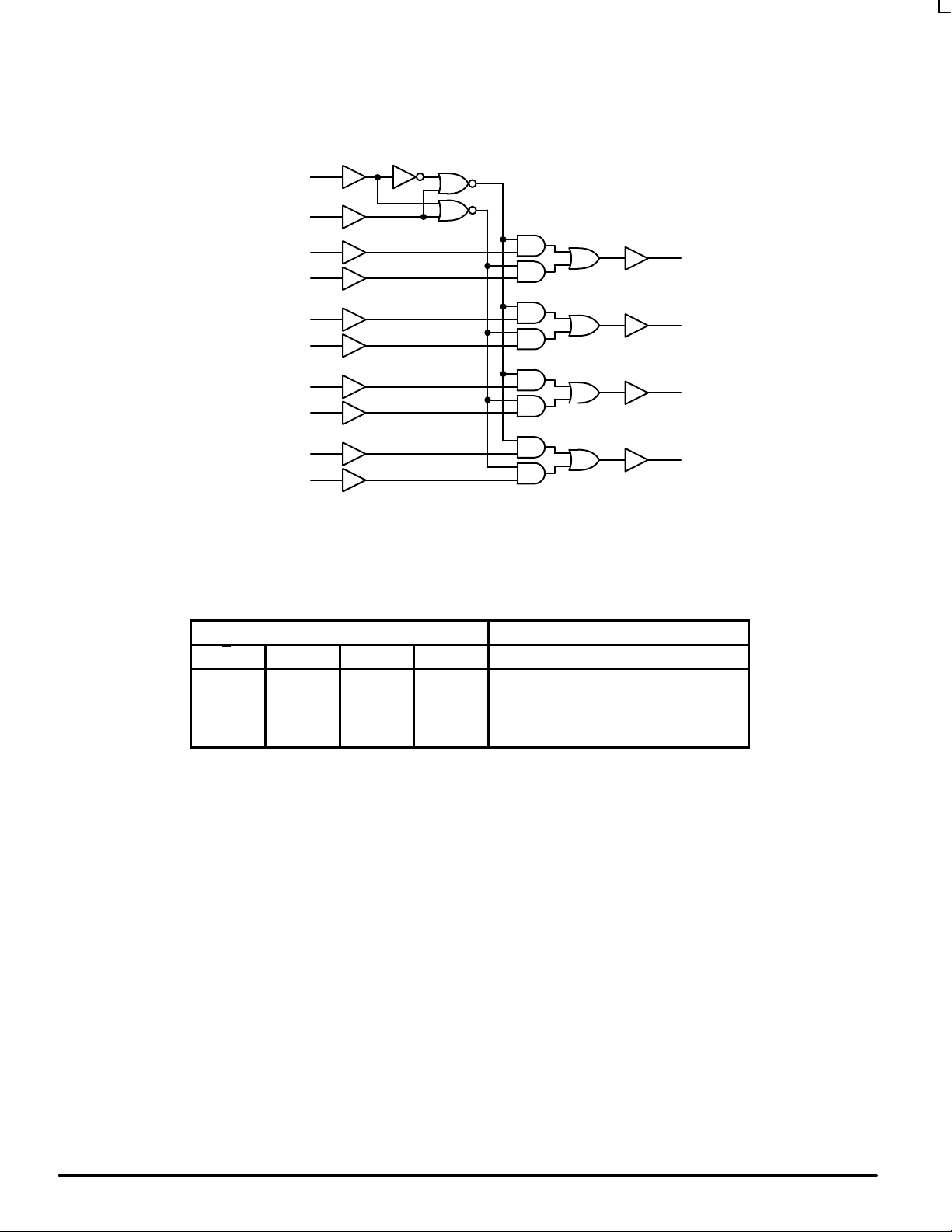
S I0a I1a Za I0b I1b Zb GND
Figure 1. 16–Lead Pinout (Top View)
I0c I1c Zc I0d I1d Zd
E
1516 14 13 12 11 10
21 34567
9
8
16–LEAD PLASTIC SOIC PACKAGE
16–LEAD PLASTIC SOIC EIAJ PACKAGE
16–LEAD PLASTIC SSOP PACKAGE
16–LEAD PLASTIC TSSOP PACKAGE
PIN NAMES
Pins
D SUFFIX
CASE 751B–05
M SUFFIX
CASE 966–01
SD SUFFIX
CASE 940B–03
DT SUFFIX
CASE 948F–01
Function
3/97
Motorola, Inc. 1997
I0n
I1n
E
S
Zn
1
REV 1
Source 0 Data Inputs
Source 1 Data Inputs
Enable Input
Select Input
Outputs
MC74LCX157
1
S
15
E
I0a
I1a
I0b
I1b
I0c
I1c
I0d
I1d
2
3
5
6
14
13
11
10
4
Za
7
Zb
12
Zc
9
Zd
Figure 2. Logic Diagram
TRUTH TABLE
Inputs Outputs
E S I0n I1n Zn
H
L
L
L
L
H = High Voltage Level; L = Low V oltage Level; X = High or Low Voltage Level ; For ICC Reasons DO NOT
FLOAT Inputs
X
H
H
L
L
X
X
X
L
H
X
L
H
X
X
L
L
H
L
H
MOTOROLA LCX DATA
2
BR1339 — REV 3
MC74LCX157
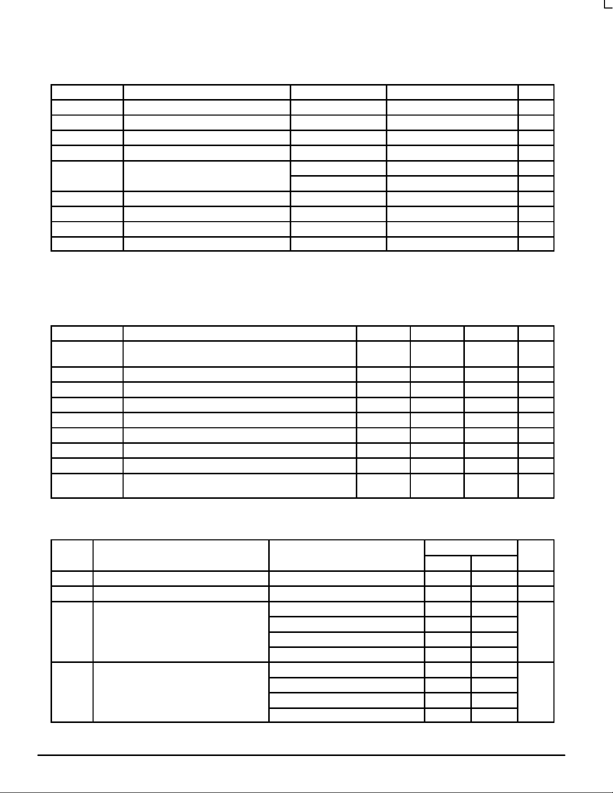
ABSOLUTE MAXIMUM RATINGS*
Symbol Parameter Value Condition Unit
V
CC
V
I
V
O
I
IK
I
OK
I
O
I
CC
I
GND
T
STG
* Absolute maximum continuous ratings are those values beyond which damage to the device may occur. Exposure to these conditions or
conditions beyond those indicated may adversely affect device reliability. Functional operation under absolute–maximum–rated conditions is
not implied.
1. Output in HIGH or LOW State. IO absolute maximum rating must be observed.
RECOMMENDED OPERATING CONDITIONS
Symbol Parameter Min Typ Max Unit
V
CC
V
I
V
O
I
OH
I
OL
I
OH
I
OL
T
A
∆t/∆V Input Transition Rise or Fall Rate, VIN from 0.8V to 2.0V ,
DC Supply Voltage –0.5 to +7.0 V
DC Input Voltage –0.5 ≤ VI ≤ +7.0 V
DC Output Voltage –0.5 ≤ VO ≤ VCC + 0.5 Note 1. V
DC Input Diode Current –50 VI < GND mA
DC Output Diode Current –50 VO < GND mA
+50 VO > V
DC Output Source/Sink Current ±50 mA
DC Supply Current Per Supply Pin ±100 mA
DC Ground Current Per Ground Pin ±100 mA
Storage Temperature Range –65 to +150 °C
Supply Voltage Operating
Data Retention Only
Input Voltage 0 5.5 V
Output Voltage (HIGH or LOW State) 0 V
HIGH Level Output Current, VCC = 3.0V – 3.6V –24 mA
LOW Level Output Current, VCC = 3.0V – 3.6V 24 mA
HIGH Level Output Current, VCC = 2.7V – 3.0V –12 mA
LOW Level Output Current, VCC = 2.7V – 3.0V 12 mA
Operating Free–Air Temperature –40 +85 °C
VCC = 3.0V
2.0
1.5
0 10 ns/V
3.3
3.3
CC
3.6
3.6
CC
mA
V
V
DC ELECTRICAL CHARACTERISTICS
TA = –40°C to +85°C
Symbol Characteristic Condition Min Max Unit
V
IH
V
IL
V
OH
V
OL
2. These values of VI are used to test DC electrical characteristics only.
LCX DATA
BR1339 — REV 3
HIGH Level Input Voltage (Note 2.) 2.7V ≤ VCC ≤ 3.6V 2.0 V
LOW Level Input Voltage (Note 2.) 2.7V ≤ VCC ≤ 3.6V 0.8 V
HIGH Level Output Voltage 2.7V ≤ VCC ≤ 3.6V; IOH = –100µA VCC– 0.2 V
VCC = 2.7V; IOH = –12mA 2.2
VCC = 3.0V; IOH = –18mA 2.4
VCC = 3.0V; IOH = –24mA 2.2
LOW Level Output Voltage 2.7V ≤ VCC ≤ 3.6V; IOL = 100µA 0.2 V
VCC = 2.7V; IOL= 12mA 0.4
VCC = 3.0V; IOL = 16mA 0.4
VCC = 3.0V; IOL = 24mA 0.55
3 MOTOROLA
 Loading...