

Motorola MC74HC299DW, MC74HC299N Datasheet
SEMICONDUCTOR TECHNICAL DATA
3–1
REV 6
Motorola, Inc. 1995
10/95
# !# $!"
# "#! %# !
High–Performance Silicon–Gate CMOS
The MC74HC299 is identical in pinout to the LS299. The device inputs are
compatible with standard CMOS outputs; with pullup resistors, they are
compatible with LSTTL outputs.
The HC299 features a multiplexed parallel input/output data port to
achieve full 8–bit handling in a 20 pin package. Due to the large output drive
capability and the 3–state feature, this device is ideally suited for interface
with bus lines in a bus–oriented system.
Two Mode–Select inputs and two Output Enable inputs a re used to
choose the mode of operation as listed in the Function Table. Synchronous
parallel loading is accomplished by taking both Mode–Select lines, S1 and
S2, high. This places the outputs in the high–impedance state, which permits
data applied to the data port to be clocked into the register. Reading out of
the register can be accomplished when the outputs are enabled. The
active–low asynchronous Reset overrides all other inputs.
• Output Drive Capability: 15 LSTTL Loads for QA through Q
H
10 LSTTL Loads for QA′ and QH′
• Outputs Directly Interface to CMOS, NMOS, and TTL
• Operating Voltage Range: 2 to 6 V
• Low Input Current: 1 µA
• High Noise Immunity Characteristic of CMOS Devices
• In Compliance with the Requirements Defined by JEDEC Standard
No. 7A
• Chip Complexity: 398 FETs or 99.5 Equivalent Gates
LOGIC DIAGRAM
7
13
6
14
5
15
4
16
8
17
11
18
12
9
1
19
2
3
PG/Q
G
PE/Q
E
PC/Q
C
PA/Q
A
Q
A
′
Q
H
′
PH/Q
H
PF/Q
F
PD/Q
D
PB/Q
B
SERIAL
DATA
INPUTS
SA (SHIFT RIGHT)
SH (SHIFT LEFT)
RESET
S
1
S
2
OE1
OE2
MODE
SELECT
OUTPUT
ENABLES
CLOCK
3–STATE
PARALLEL DATA PORT
(INPUTS/OUTPUTS)
SERIAL DATA
OUTPUTS
PIN 20 = V
CC
PIN 10 = GND
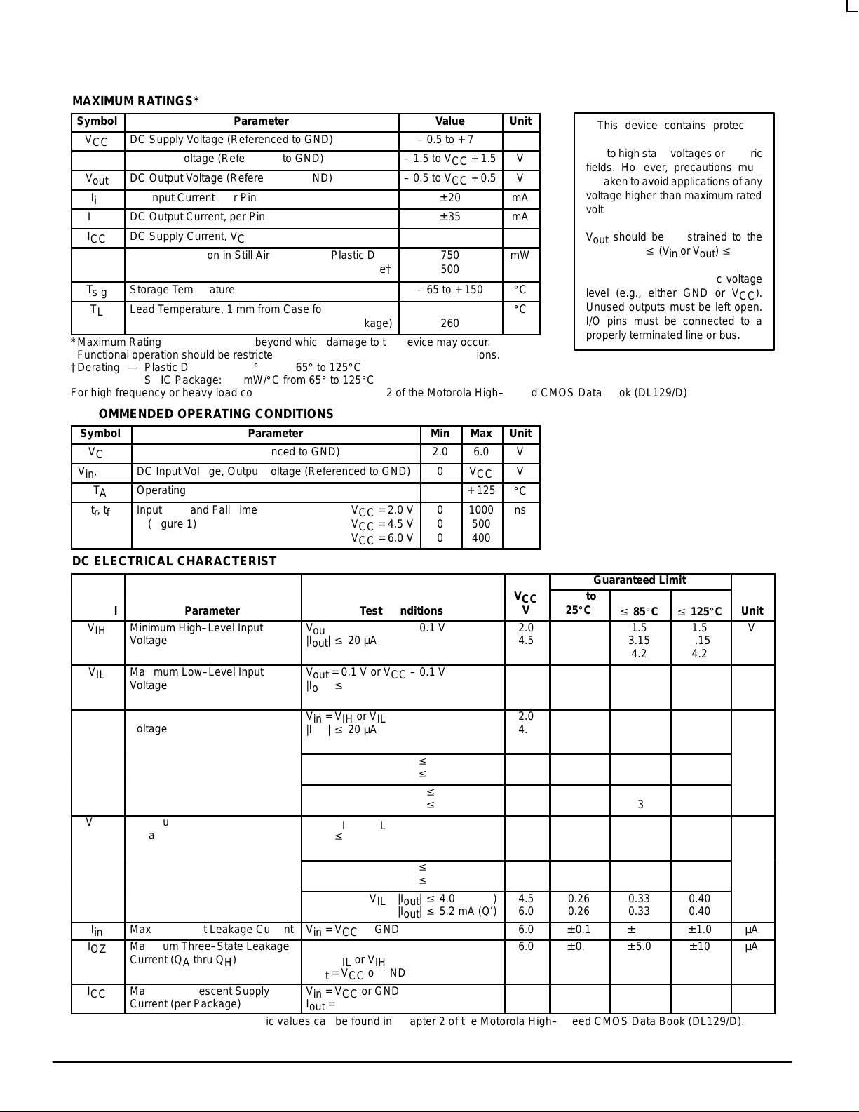
PIN ASSIGNMENT
PC/Q
C
PG/Q
G
OE2
OE1
S1
GND
RESET
Q
A
′
PA/Q
A
PE/QE5
4
3
2
1
10
9
8
7
6
14
15
16
17
18
19
20
11
12
13
PH/Q
H
Q
H
′
S
H
S2
V
CC
S
A
CLOCK
PB/Q
B
PD/Q
D
PF/Q
F
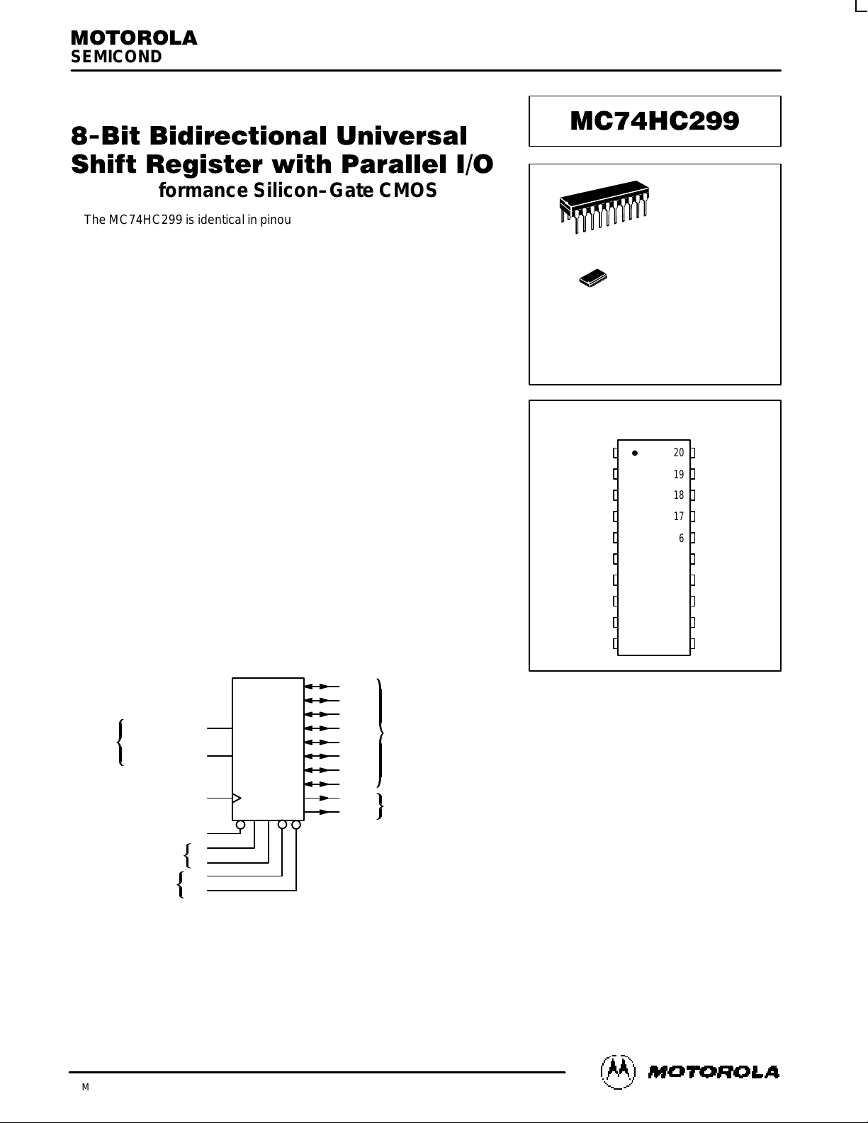
DW SUFFIX
SOIC PACKAGE
CASE 751D–04
N SUFFIX
PLASTIC PACKAGE
CASE 738–03
ORDERING INFORMATION
MC74HCXXXN
MC74HCXXXDW
Plastic
SOIC
1
20
1
20
MC74HC299
MOTOROLA High–Speed CMOS Logic Data
DL129 — Rev 6
3–2
MAXIMUM RATINGS*
Symbol
Parameter
Value
Unit
V
CC
DC Supply Voltage (Referenced to GND)
– 0.5 to + 7.0
V
V
in
DC Input Voltage (Referenced to GND)
– 1.5 to VCC + 1.5
V
V
out
DC Output Voltage (Referenced to GND)
– 0.5 to VCC + 0.5
V
I
in
DC Input Current, per Pin
± 20
mA
I
out
DC Output Current, per Pin
± 35
mA
I
CC
DC Supply Current, VCC and GND Pins
± 75
mA
P
D
Power Dissipation in Still Air Plastic DIP†
SOIC Package†
750
500
mW
T
stg
Storage Temperature
– 65 to + 150
_
C
T
L
Lead Temperature, 1 mm from Case for 10 Seconds
(Plastic DIP or SOIC Package)
260
_
C
*Maximum Ratings are those values beyond which damage to the device may occur.
Functional operation should be restricted to the Recommended Operating Conditions.
†Derating — Plastic DIP: – 10 mW/_C from 65_ to 125_C
SOIC Package: – 7 mW/_C from 65_ to 125_C
For high frequency or heavy load considerations, see Chapter 2 of the Motorola High–Speed CMOS Data Book (DL129/D).
RECOMMENDED OPERATING CONDITIONS
Symbol
Parameter
Min
Max
Unit
V
CC
DC Supply Voltage (Referenced to GND)
2.0
6.0
V
Vin, V
out
DC Input Voltage, Output Voltage (Referenced to GND)
0
V
CC
V
T
A
Operating Temperature, All Package Types
– 55
+ 125
_
C
tr, t
f
Input Rise and Fall Time VCC = 2.0 V
(Figure 1) VCC = 4.5 V
VCC = 6.0 V
0
0
0
1000
500
400
ns
DC ELECTRICAL CHARACTERISTICS (Voltages Referenced to GND)
Guaranteed Limit
Symbol
Parameter
Test Conditions
V
CC
V
– 55 to
25_C
v
85_C
v
125_C
Unit
V
IH
Minimum High–Level Input
Voltage
V
out
= 0.1 V or VCC – 0.1 V
|I
out
| v 20 µA
2.0
4.5
6.0
1.5
3.15
4.2
1.5
3.15
4.2
1.5
3.15
4.2
V
V
IL
Maximum Low–Level Input
Voltage
V
out
= 0.1 V or VCC – 0.1 V
|I
out
| v 20 µA
2.0
4.5
6.0
0.3
0.9
1.2
0.3
0.9
1.2
0.3
0.9
1.2
V
Vin = VIH or V
IL
|I
out
| v 20 µA
2.0
4.5
6.0
1.9
4.4
5.9
1.9
4.4
5.9
1.9
4.4
5.9
Vin = VIH or VIL|I
out
| v 6.0 mA (P/Q)
|I
out
| v 7.8 mA (P/Q)
4.5
6.0
3.98
5.48
3.84
5.34
3.70
5.20
Vin = VIH or VIL|I
out
| v 4.0 mA (Q′)
|I
out
| v 5.2 mA (Q′)
4.5
6.0
3.98
5.48
3.84
5.34
3.70
5.20
Vin = VIH or V
IL
|I
out
| v 20 µA
2.0
4.5
6.0
0.1
0.1
0.1
0.1
0.1
0.1
0.1
0.1
0.1
Vin = VIH or VIL|I
out
| v 6.0 mA (P/Q)
|I
out
| v 7.8 mA (P/Q)
4.5
6.0
0.26
0.26
0.33
0.33
0.40
0.40
Vin = VIH or VIL|I
out
| v 4.0 mA (Q′)
|I
out
| v 5.2 mA (Q′)
4.5
6.0
0.26
0.26
0.33
0.33
0.40
0.40
I
in
Maximum Input Leakage Current
Vin = VCC or GND
6.0
± 0.1
± 1.0
± 1.0
µA
I
OZ
Maximum Three–State Leakage
Current (QA thru QH)
Output in High–Impedance State
Vin = VIL or V
IH
V
out
= VCC or GND
6.0
± 0.5
± 5.0
± 10
µA
I
CC
Maximum Quiescent Supply
Current (per Package)
Vin = VCC or GND
I
out
= 0 µA
6.0
8
80
160
µA
NOTE: Information on typical parametric values can be found in Chapter 2 of the Motorola High–Speed CMOS Data Book (DL129/D).
This device contains protection
circuitry to guard against damage
due to high static voltages or electric
fields. However, precautions must
be taken to avoid applications of any
voltage higher than maximum rated
voltages to this high–impedance circuit. For proper operation, Vin and
V
out
should be constrained to the
range GND v (Vin or V
out
) v VCC.
Unused inputs must always be
tied to an appropriate logic voltage
level (e.g., either GND or VCC).
Unused outputs must be left open.
I/O pins must be connected to a
properly terminated line or bus.
V
V
Minimum High–Level Output
OH
Voltage
Maximum Low–Level Output
OL
Voltage
V
V
MC74HC299
High–Speed CMOS Logic Data
DL129 — Rev 6
3–3 MOTOROLA
AC ELECTRICAL CHARACTERISTICS (C
L
= 50 pF, Input tr = tf = 6 ns)
Guaranteed Limit
Symbol
Parameter
V
CC
V
– 55 to
25_C
v
85_C
v
125_C
Unit
f
max
Maximum Clock Frequency (50% Duty Cycle)
(Figures 1 and 5)
2.0
4.5
6.0
5.0
25
29
4.0
20
24
3.4
17
20
MHz
t
PLH
,
t
PHL
Maximum Propagation Delay, Clock to QA′ or QH′
(Figures 1 and 5)
2.0
4.5
6.0
170
34
29
215
43
37
255
51
43
ns
t
PLH
,
t
PHL
Maximum Propagation Delay, Clock to QA thru Q
H
(Figures 1 and 5)
2.0
4.5
6.0
160
32
27
200
40
34
240
48
41
ns
t
PHL
Maximum Propagation Delay, Reset to QA or Q
H
(Figures 2 and 5)
2.0
4.5
6.0
175
35
30
220
44
37
265
53
45
ns
t
PHL
Maximum Propagation Delay, Reset to QA′ thru QH′
(Figures 2 and 5)
2.0
4.5
6.0
190
38
32
240
48
41
285
57
48
ns
t
PLZ
,
t
PHZ
Maximum Propagation Delay, OE1, OE2, S1, or S2 to QA thru Q
H
(Figures 3 and 6)
2.0
4.5
6.0
150
30
26
190
38
33
225
45
38
ns
t
PZL
,
t
PZH
Maximum Propagation Delay, OE1, OE2, S1, or S2 to QA thru Q
H
(Figures 3 and 6)
2.0
4.5
6.0
150
30
26
190
38
33
225
45
38
ns
t
TLH
,
t
THL
Maximum Output Transition Time, QA thru Q
H
(Figures 1 and 5)
2.0
4.5
6.0
60
12
10
75
15
13
90
18
15
ns
t
TLH
,
t
THL
Maximum Output Transition Time, QA′ or QH′
(Figures 1 and 5)
2.0
4.5
6.0
75
15
13
95
19
16
110
22
19
ns
C
in
Maximum Input Capacitance
—
10
10
10
pF
C
out
Maximum Three–State Output Capacitance
(Output in High–Impedance State), QA thru Q
H
—
15
15
15
pF
NOTES:
1. For propagation delays with loads other than 50 pF, see Chapter 2 of the Motorola High–Speed CMOS Data Book (DL129/D).
2. Information on typical parametric values can be found in Chapter 2 of the Motorola High–Speed CMOS Data Book (DL129/D).
Typical @ 25°C, VCC = 5.0 V
240
*Used to determine the no–load dynamic power consumption: PD = CPD V
CC
2
f + ICC VCC. For load considerations, see Chapter 2 of the
Motorola High–Speed CMOS Data Book (DL129/D).
C
PD
Power Dissipation Capacitance (Per Package)*, Outputs Enabled
pF
 Loading...