

Motorola MC74HC251D, MC74HC251N Datasheet
SEMICONDUCTOR TECHNICAL DATA
1
REV 6
Motorola, Inc. 1995
10/95
"! ! !
"!$ #!
!! "!"!
High–Performance Silicon–Gate CMOS
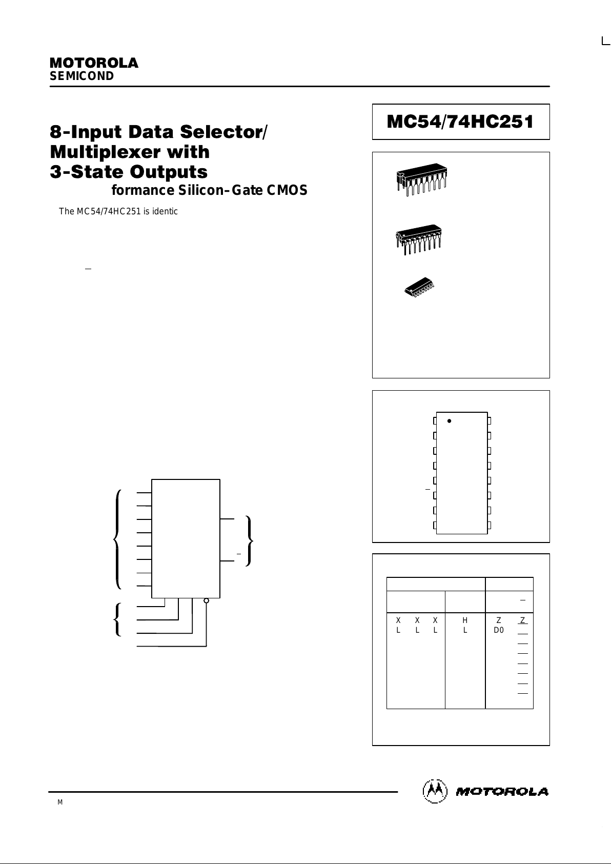
The MC54/74HC251 is identical in pinout to the LS251. The device inputs
are compatible with standard CMOS outputs; with pullup resistors, they are
compatible with LSTTL outputs.
This device selects one of the eight binary Data Inputs, as determined by
the Address Inputs. The Output Enable pin must be a low level for the
selected data to appear at the outputs. If Output Enable is high, both the Y
and the Y
outputs are in the high–impedance state. This 3–state feature
allows the HC251 to be used in bus–oriented systems.
The HC251 is similar i n function t o the HC151 which does not have
3–state outputs.
• Output Drive Capability: 10 LSTTL Loads
• Outputs Directly Interface to CMOS, NMOS, and TTL
• Operating Voltage Range: 2 to 6 V
• Low Input Current: 1 µA
• High Noise Immunity Characteristic of CMOS Devices
• In Compliance with the Requirements Defined by JEDEC Standard
No. 7A
• Chip Complexity: 134 FETs or 33.5 Equivalent Gates
LOGIC DIAGRAM
D0
D1
D2
D3
D4
D5
D6
D7
A0
A1
A2
OUTPUT ENABLE
Y
Y
DATA
OUTPUTS
DATA
INPUTS
ADDRESS
INPUTS
5
6
4
3
2
1
15
14
13
12
11
10
9
7
PIN 16 = V
CC
PIN 8 = GND
PIN ASSIGNMENT
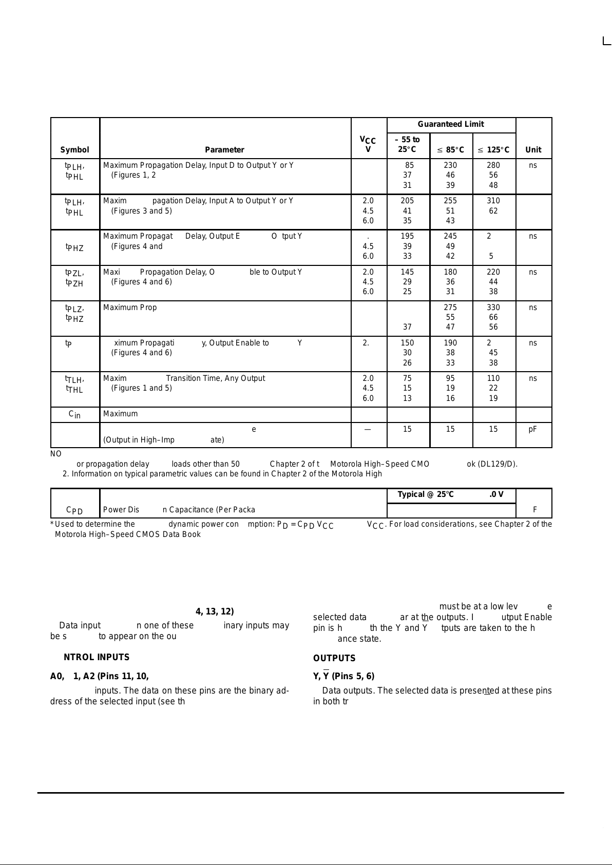
FUNCTION TABLE
Inputs Outputs
Output
A2 A1 A0 Enable Y Y
X X X H Z Z
L L L L D0 D0
L L H L D1 D1
L H L L D2 D2
L H H L D3 D3
H L L L D4 D4
H L H L D5 D5
H H L L D6 D6
H H H L D7 D7
Z = high impedance
D0, D1, …, D7 = the level of the respective
D input.
13
14
15
16
9
10
11
125
4
3
2
1
8
7
6
D7
D6
D5
D4
V
CC
A2
A1
A0
D0
D1
D2
D3
GND
OUTPUT
ENABLE
Y
Y
D SUFFIX
SOIC PACKAGE
CASE 751B–05
N SUFFIX
PLASTIC PACKAGE
CASE 648–08
ORDERING INFORMATION
MC54HCXXXJ
MC74HCXXXN
MC74HCXXXD
Ceramic
Plastic
SOIC
1
16
1
16
J SUFFIX
CERAMIC PACKAGE
CASE 620–10
1
16
MC54/74HC251
MOTOROLA High–Speed CMOS Logic Data
DL129 — Rev 6
2
MAXIMUM RATINGS*
Symbol
Parameter
Value
Unit
V
CC
DC Supply Voltage (Referenced to GND)
– 0.5 to + 7.0
V
V
in
DC Input Voltage (Referenced to GND)
– 1.5 to VCC + 1.5
V
V
out
DC Output Voltage (Referenced to GND)
– 0.5 to VCC + 0.5
V
I
in
DC Input Current, per Pin
± 25
mA
I
out
DC Output Current, per Pin
± 50
mA
I
CC
DC Supply Current, VCC and GND Pins
± 75
mA
P
D
Power Dissipation in Still Air,Plastic or Ceramic DIP†
SOIC Package†
750
500
mW
T
stg
Storage Temperature
– 65 to + 150
_
C
T
L
Lead Temperature, 1 mm from Case for 10 Seconds
(Plastic DIP or SOIC Package)
(Ceramic DIP)
260
300
_
C
*Maximum Ratings are those values beyond which damage to the device may occur.
Functional operation should be restricted to the Recommended Operating Conditions.
†Derating — Plastic DIP: – 10 mW/_C from 65_ to 125_C
Ceramic DIP: – 10 mW/_C from 100_ to 125_C
SOIC Package: – 7 mW/_C from 65_ to 125_C
For high frequency or heavy load considerations, see Chapter 2 of the Motorola High–Speed CMOS Data Book (DL129/D).
RECOMMENDED OPERATING CONDITIONS
Symbol
Parameter
Min
Max
Unit
V
CC
DC Supply Voltage (Referenced to GND)
2.0
6.0
V
Vin, V
out
DC Input Voltage, Output Voltage (Referenced to GND)
0
V
CC
V
T
A
Operating Temperature, All Package Types
– 55
+ 125
_
C
tr, t
f
Input Rise and Fall Time VCC = 2.0 V
(Figure 1) VCC = 4.5 V
VCC = 6.0 V
0
0
0
1000
500
400
ns
DC ELECTRICAL CHARACTERISTICS (Voltages Referenced to GND)
Guaranteed Limit
Symbol
Parameter
Test Conditions
V
CC
V
– 55 to
25_C
v
85_Cv 125_C
Unit
V
IH
Minimum High–Level Input
Voltage
V
out
= 0.1 V or VCC – 0.1 V
|I
out
| v 20 µA
2.0
4.5
6.0
1.5
3.15
4.2
1.5
3.15
4.2
1.5
3.15
4.2
V
V
IL
Maximum Low–Level Input
Voltage
V
out
= 0.1 V or VCC – 0.1 V
|I
out
| v 20 µA
2.0
4.5
6.0
0.3
0.9
1.2
0.3
0.9
1.2
0.3
0.9
1.2
V
V
OH
Minimum High–Level Output
Voltage
Vin = VIH or V
IL
|I
out
| v 20 µA
2.0
4.5
6.0
1.9
4.4
5.9
1.9
4.4
5.9
1.9
4.4
5.9
V
Vin = VIH or VIL|I
out
| v 4.0 mA
|I
out
| v 5.2 mA
4.5
6.0
3.98
5.48
3.84
5.34
3.70
5.20
V
OL
Maximum Low–Level Output
Voltage
Vin = VIH or V
IL
|I
out
| v 20 µA
2.0
4.5
6.0
0.1
0.1
0.1
0.1
0.1
0.1
0.1
0.1
0.1
V
Vin = VIH or VIL|I
out
| v 4.0 mA
|I
out
| v 5.2 mA
4.5
6.0
0.26
0.26
0.33
0.33
0.40
0.40
I
in
Maximum Input Leakage Current
Vin = VCC or GND
6.0
± 0.1
± 1.0
± 1.0
µA
I
OZ
Maximum Three–State
Leakage Current
Output in High–Impedance State
Vin = VIL or V
IH
V
out
= VCC or GND
6.0
± 0.5
± 5.0
± 10
µA
I
CC
Maximum Quiescent Supply
Current (per Package)
Vin = VCC or GND
I
out
= 0 µA
6.0
8
80
160
µA
NOTE: Information on typical parametric values can be found in Chapter 2 of the Motorola High–Speed CMOS Data Book (DL129/D).
This device contains protection
circuitry to guard against damage
due to high static voltages or electric
fields. However, precautions must
be taken to avoid applications of any
voltage higher than maximum rated
voltages to this high–impedance circuit. For proper operation, Vin and
V
out
should be constrained to the
range GND v (Vin or V
out
) v VCC.
Unused inputs must always be
tied to an appropriate logic voltage
level (e.g., either GND or VCC).
Unused outputs must be left open.
MC54/74HC251
High–Speed CMOS Logic Data
DL129 — Rev 6
3 MOTOROLA
AC ELECTRICAL CHARACTERISTICS (C
L
= 50 pF, Input tr = tf = 6 ns)
Guaranteed Limit
Symbol
Parameter
V
CC
V
– 55 to
25_C
v
85_Cv 125_C
Unit
t
PLH
,
t
PHL
Maximum Propagation Delay, Input D to Output Y or Y
(Figures 1, 2 and 5)
2.0
4.5
6.0
185
37
31
230
46
39
280
56
48
ns
t
PLH
,
t
PHL
Maximum Propagation Delay, Input A to Output Y or Y
(Figures 3 and 5)
2.0
4.5
6.0
205
41
35
255
51
43
310
62
53
ns
t
PLZ
,
t
PHZ
Maximum Propagation Delay, Output Enable to Output Y
(Figures 4 and 6)
2.0
4.5
6.0
195
39
33
245
49
42
295
59
50
ns
t
PZL
,
t
PZH
Maximum Propagation Delay, Output Enable to Output Y
(Figures 4 and 6)
2.0
4.5
6.0
145
29
25
180
36
31
220
44
38
ns
t
PLZ
,
t
PHZ
Maximum Propagation Delay, Output Enable to Output Y
(Figures 4 and 6)
2.0
4.5
6.0
220
44
37
275
55
47
330
66
56
ns
t
PZL
,
t
PZH
Maximum Propagation Delay, Output Enable to Output Y
(Figures 4 and 6)
2.0
4.5
6.0
150
30
26
190
38
33
225
45
38
ns
t
TLH
,
t
THL
Maximum Output Transition Time, Any Output
(Figures 1 and 5)
2.0
4.5
6.0
75
15
13
95
19
16
110
22
19
ns
C
in
Maximum Input Capacitance
—
10
10
10
pF
C
out
Maximum Three–State Output Capacitance
(Output in High–Impedance
State)
—
15
15
15
pF
NOTES:
1. For propagation delays with loads other than 50 pF, see Chapter 2 of the Motorola High–Speed CMOS Data Book (DL129/D).
2. Information on typical parametric values can be found in Chapter 2 of the Motorola High–Speed CMOS Data Book (DL129/D).
Typical @ 25°C, VCC = 5.0 V
C
PD
Power Dissipation Capacitance (Per Package)*
36
pF
*Used to determine the no–load dynamic power consumption: PD = CPD V
CC
2
f + ICC VCC. For load considerations, see Chapter 2 of the
Motorola High–Speed CMOS Data Book (DL129/D).
PIN DESCRIPTIONS
INPUTS
D0, D1, …, D7 (Pins 4, 3, 2, 1, 15, 14, 13, 12)
Data inputs. Data on one of these eight binary inputs may
be selected to appear on the output.
CONTROL INPUTS
A0, A1, A2 (Pins 11, 10, 9)
Address inputs. The data on these pins are the binary ad-
dress of the selected input (see the Function Table).
Output Enable (Pin 7)
Output Enable. This input pin must be at a low level for the
selected data to appear at the outputs. If the Output Enable
pin is high, both the Y and Y
outputs are taken to the high–
impedance state.
OUTPUTS
Y, Y
(Pins 5, 6)
Data outputs. The selected data is presented at these pins
in both true (Y output) and complemented (Y
output) forms.
 Loading...