

Datasheet MC74HC245AFER, MC74HC245ADW, MC74HC245ADWR2, MC74HC245AF, MC74HC245ADT Datasheet (MOTOROLA)
...
Semiconductor Components Industries, LLC, 2000
March, 2000 – Rev. 8
1 Publication Order Number:
MC74HC245A/D
MC74HC245A
Octal 3-State Noninverting
Bus Transceiver
High–Performance Silicon–Gate CMOS
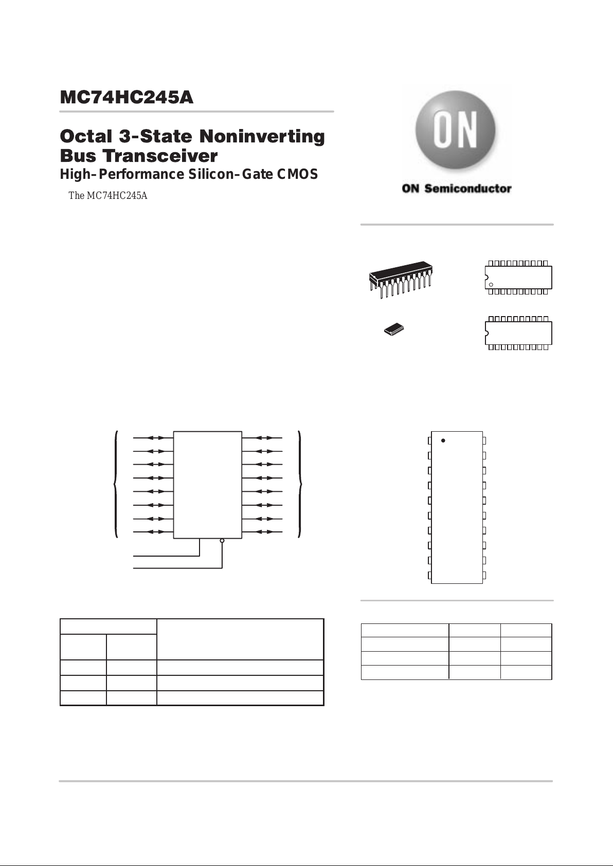
The MC74HC245A is identical in pinout to the LS245. The device
inputs are compatible with standard CMOS outputs; with pullup
resistors, they are compatible with LSTTL outputs.
The HC245A is a 3–state noninverting transceiver that is used for
2–way asynchronous communication between data buses. The device
has an active–low Output Enable pin, which is used to place the I/O
ports into high–impedance states. The Direction control determines
whether data flows from A to B or from B to A.
• Output Drive Capability: 15 LSTTL Loads
• Outputs Directly Interface to CMOS, NMOS, and TTL
• Operating Voltage Range: 2 to 6 V
• Low Input Current: 1 µA
• High Noise Immunity Characteristic of CMOS Devices
• In Compliance with the Requirements Defined by JEDEC Standard
No. 7A
• Chip Complexity: 308 FETs or 77 Equivalent Gates
LOGIC DIAGRAM
A
DATA
PORT
A8
A7
A6
A5
A3
A4
A2
A1
9
8
7
6
5
4
3
2
DIRECTION
OUTPUT ENABLE
1
19
PIN 10 = GND
PIN 20 = V
CC
18
17
16
15
14
13
12
11
B1
B2
B3
B4
B5
B6
B7
B8
B
DATA
PORT
FUNCTION TABLE
Control Inputs
Output
Enable
Direction
Operation
L L Data Transmitted from Bus B to Bus A
L H Data Transmitted from Bus A to Bus B
H X Buses Isolated (High–Impedance State)
X = don’t care
http://onsemi.com
MARKING
DIAGRAMS
1
20
A = Assembly Location
WL = Wafer Lot
YY = Year
WW = Work Week
SOIC WIDE–20
DW SUFFIX
CASE 751D
HC245A
AWLYYWW
PDIP–20
N SUFFIX
CASE 738
1
20
MC74HC245AN
AWLYYWW
1
20
1
20
Device Package Shipping
ORDERING INFORMATION
MC74HC245AN PDIP–20 1440 / Box
MC74HC245ADW SOIC–WIDE
38 / Rail
MC74HC245ADWR2 SOIC–WIDE 1000 / Reel
PIN ASSIGNMENT
A5
A3
A2
A1
DIRECTION
GND
A8
A7
A6
A4 5
4
3
2
1
10
9
8
7
6
14
15
16
17
18
19
20
11
12
13
B3
B2
B1
OUTPUT ENABLE
V
CC
B8
B7
B6
B5
B4
MC74HC245A
http://onsemi.com
2
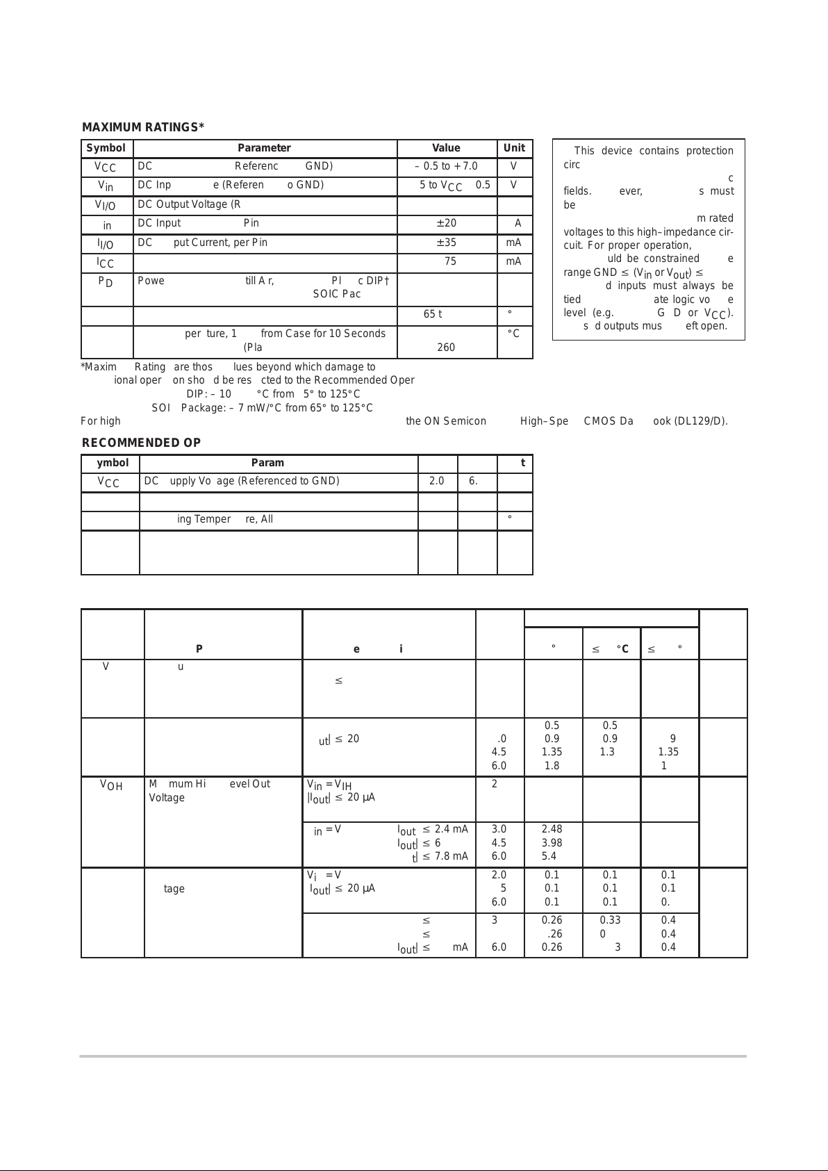
MAXIMUM RATINGS*
Symbol
Parameter
Value
Unit
V
CC
DC Supply Voltage (Referenced to GND)
– 0.5 to + 7.0
V
V
in
DC Input Voltage (Referenced to GND)
– 0.5 to VCC + 0.5
V
V
I/O
DC Output Voltage (Referenced to GND)
– 0.5 to VCC + 0.5
V
I
in
DC Input Current, per Pin
± 20
mA
I
I/O
DC Output Current, per Pin
± 35
mA
I
CC
DC Supply Current, VCC and GND Pins
± 75
mA
ÎÎ
Î
P
D
ОООООООООООО
Î
Power Dissipation in Still Air, Plastic DIP†
SOIC Package†
ÎÎÎ
Î
750
500
Î
Î
mW
T
stg
Storage Temperature
– 65 to + 150
_
C
T
L
Lead Temperature, 1 mm from Case for 10 Seconds
(Plastic DIP or SOIC Package)
260
_
C
*Maximum Ratings are those values beyond which damage to the device may occur.
Functional operation should be restricted to the Recommended Operating Conditions.
†Derating — Plastic DIP: – 10 mW/_C from 65_ to 125_C
SOIC Package: – 7 mW/_C from 65_ to 125_C
For high frequency or heavy load considerations, see Chapter 2 of the ON Semiconductor High–Speed CMOS Data Book (DL129/D).
RECOMMENDED OPERATING CONDITIONS
Symbol
Parameter
Min
ÎÎ
Max
Unit
V
CC
DC Supply Voltage (Referenced to GND)
2.0
ÎÎ
6.0
V
Vin, V
out
DC Input Voltage, Output Voltage (Referenced to GND)
0
ÎÎ
V
CC
V
T
A
Operating Temperature, All Package Types
– 55
ÎÎ
+ 125
_
C
ÎÎ
Î
tr, t
f
ООООООООООООО
Î
Input Rise and Fall Time VCC = 2.0 V
(Figure 1) VCC = 4.5 V
VCC = 6.0 V
Î
Î
0
0
0
ÎÎ
ÎÎ
1000
500
400
Î
Î
ns
DC ELECTRICAL CHARACTERISTICS (Voltages Referenced to GND)
Guaranteed Limit
ÎÎ
Î
Symbol
ООООООО
Î
Parameter
ООООООО
Î
Test Conditions
ÎÎ
Î
V
CC
V
ÎÎ
Î
– 55 to
25_C
ÎÎÎ
Î
Î
Î
v
85_C
ÎÎ
Î
v
125_C
Î
Î
Unit
ÎÎ
Î
ÎÎ
Î
V
IH
ООООООО
Î
ООООООО
Î
Minimum High–Level Input
Voltage
ООООООО
Î
ООООООО
Î
V
out
= VCC – 0.1 V
|I
out
| v 20 µA
ÎÎ
Î
ÎÎ
Î
2.0
3.0
4.5
6.0
ÎÎ
Î
ÎÎ
Î
1.5
2.1
3.15
4.2
ÎÎÎ
Î
Î
Î
Î
Î
Î
1.5
2.1
3.15
4.2
ÎÎ
Î
ÎÎ
Î
1.5
2.1
3.15
4.2
Î
Î
Î
Î
V
ÎÎ
Î
V
IL
ООООООО
Î
Maximum Low–Level Input
Voltage
ООООООО
Î
V
out
= 0.1 V
|I
out
| v 20 µA
ÎÎ
Î
2.0
3.0
4.5
6.0
ÎÎ
Î
0.5
0.9
1.35
1.8
ÎÎÎ
Î
Î
Î
0.5
0.9
1.35
1.8
ÎÎ
Î
0.5
0.9
1.35
1.8
Î
Î
V
ÎÎ
Î
ÎÎ
Î
V
OH
ООООООО
Î
ООООООО
Î
Minimum High–Level Output
Voltage
ООООООО
Î
ООООООО
Î
Vin = V
IH
|I
out
| v 20 µA
ÎÎ
Î
ÎÎ
Î
2.0
4.5
6.0
ÎÎ
Î
ÎÎ
Î
1.9
4.4
5.9
ÎÎÎ
Î
Î
Î
Î
Î
Î
1.9
4.4
5.9
ÎÎ
Î
ÎÎ
Î
1.9
4.4
5.9
Î
Î
Î
Î
V
ÎÎÎОООООООÎООООООО
Î
Vin = V
IH
|I
out
| v 2.4 mA
|I
out
| v 6.0 mA
|I
out
| v 7.8 mA
ÎÎ
Î
3.0
4.5
6.0
ÎÎ
Î
2.48
3.98
5.48
ÎÎÎ
Î
Î
Î
2.34
3.84
5.34
ÎÎ
Î
2.2
3.7
5.2
Î
Î
ÎÎ
Î
V
OL
ООООООО
Î
Maximum Low–Level Output
Voltage
ООООООО
Î
Vin = V
IL
|I
out
| v 20 µA
ÎÎ
Î
2.0
4.5
6.0
ÎÎ
Î
0.1
0.1
0.1
ÎÎÎ
Î
Î
Î
0.1
0.1
0.1
ÎÎ
Î
0.1
0.1
0.1
Î
Î
V
ÎÎÎОООООООÎООООООО
Î
Vin = V
IL
|I
out
| v 2.4 mA
|I
out
| v 6.0 mA
|I
out
| v 7.8 mA
ÎÎ
Î
3.0
4.5
6.0
ÎÎ
Î
0.26
0.26
0.26
ÎÎÎ
Î
Î
Î
0.33
0.33
0.33
ÎÎ
Î
0.4
0.4
0.4
Î
Î
This device contains protection
circuitry to guard against damage
due to high static voltages or electric
fields. However, precautions must
be taken to avoid applications of any
voltage higher than maximum rated
voltages to this high–impedance circuit. For proper operation, Vin and
V
out
should be constrained to the
range GND v (Vin or V
out
) v VCC.
Unused inputs must always be
tied to an appropriate logic voltage
level (e.g., either GND or VCC).
Unused outputs must be left open.
MC74HC245A
http://onsemi.com
3
DC ELECTRICAL CHARACTERISTICS (Voltages Referenced to GND)
Guaranteed Limit
Unit
v
125_C
ÎÎÎ
v
85_C
– 55 to
25_C
V
CC
V
Test Conditions
Parameter
Symbol
ÎÎ
Î
I
in
ООООООО
Î
Maximum Input Leakage
Current
ООООООО
Î
Vin = VCC or GND
ÎÎ
Î
6.0
ÎÎ
Î
± 0.1
ÎÎÎ
Î
Î
Î
± 1.0
ÎÎ
Î
± 1.0
Î
Î
µA
ÎÎ
Î
I
OZ
ООООООО
Î
Maximum Three–State
Leakage Current
ООООООО
Î
Output in High–Impedance State
Vin = VIL or V
IH
V
out
= VCC or GND
ÎÎ
Î
6.0
ÎÎ
Î
± 0.5
ÎÎÎ
Î
Î
Î
± 5.0
ÎÎ
Î
± 10
Î
Î
µA
ÎÎ
Î
I
CC
ООООООО
Î
Maximum Quiescent Supply
Current (per Package)
ООООООО
Î
Vin = VCC or GND
I
out
= 0 µA
ÎÎ
Î
6.0
ÎÎ
Î
4.0
ÎÎÎ
Î
Î
Î
40
ÎÎ
Î
160
Î
Î
µA
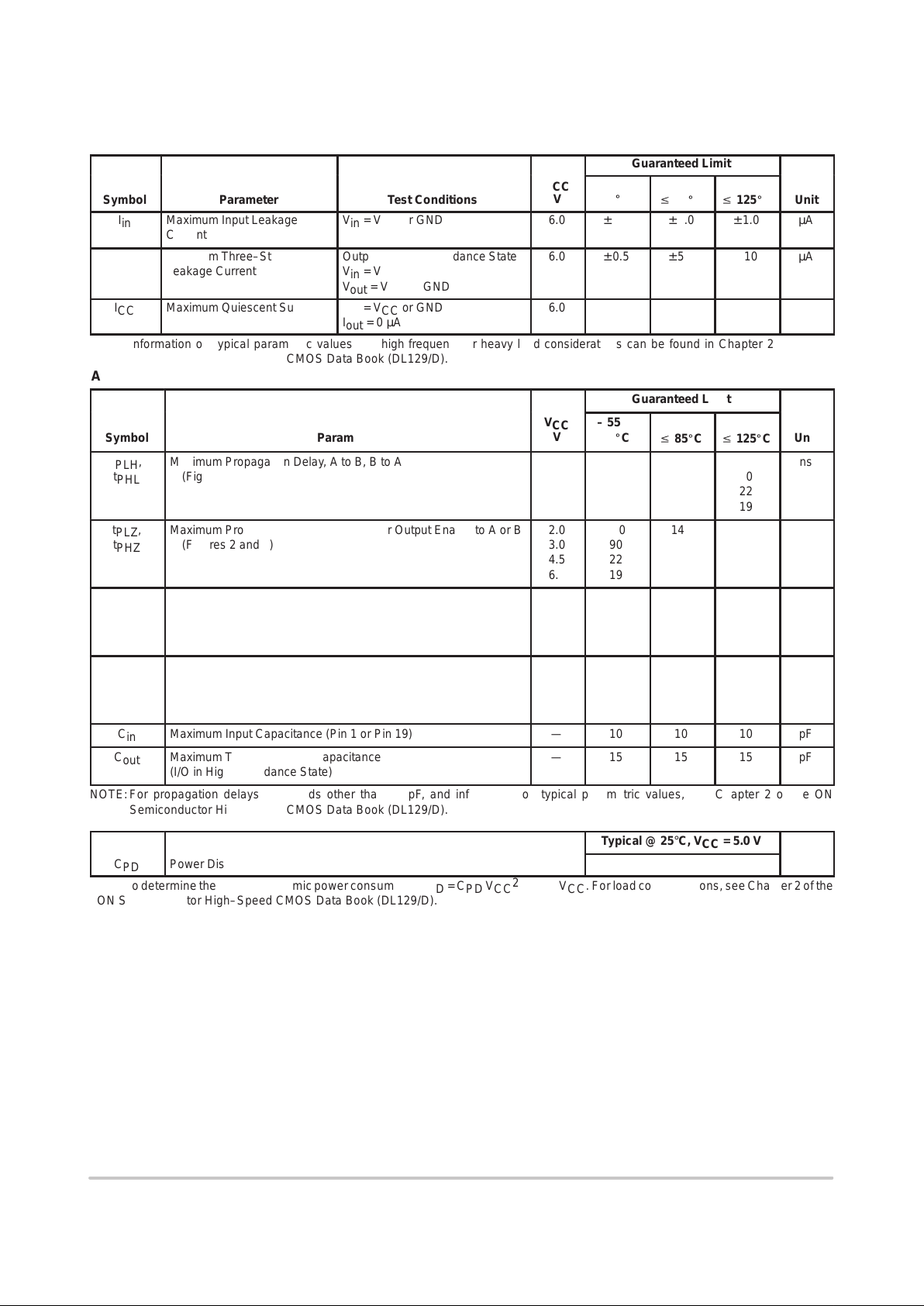
NOTE: Infor mation on typ ical p arametr ic va lues and high frequency or heavy load considerations can be found in Chapter 2 of the ON
Semiconductor High–Speed CMOS Data Book (DL129/D).
AC ELECTRICAL CHARACTERISTICS (C
L
= 50 pF, Input tr = tf = 6 ns)
Guaranteed Limit
ÎÎÎ
Î
Symbol
ОООООООООООООО
Î
Parameter
ÎÎ
Î
V
CC
V
ÎÎ
Î
– 55 to
25_C
ÎÎÎ
Î
Î
Î
v
85_C
ÎÎ
Î
v
125_C
Î
Î
Unit
ÎÎÎ
Î
ÎÎÎ
Î
t
PLH
,
t
PHL
ОООООООООООООО
Î
ОООООООООООООО
Î
Maximum Propagation Delay, A to B, B to A
(Figures 1 and 3)
ÎÎ
Î
ÎÎ
Î
2.0
3.0
4.5
6.0
ÎÎ
Î
ÎÎ
Î
75
55
15
13
ÎÎÎ
Î
Î
Î
Î
Î
Î
95
70
19
16
ÎÎ
Î
ÎÎ
Î
110
80
22
19
Î
Î
Î
Î
ns
ÎÎÎ
Î
t
PLZ
,
t
PHZ
ОООООООООООООО
Î
Maximum Propagation Delay, Direction or Output Enable to A or B
(Figures 2 and 4)
ÎÎ
Î
2.0
3.0
4.5
6.0
ÎÎ
Î
110
90
22
19
ÎÎÎ
Î
Î
Î
140
110
28
24
ÎÎ
Î
165
130
33
28
Î
Î
ns
ÎÎÎ
Î
ÎÎÎ
Î
t
PZL
,
t
PZH
ОООООООООООООО
Î
ОООООООООООООО
Î
Maximum Propagation Delay, Output Enable to A or B
(Figures 2 and 4)
ÎÎ
Î
ÎÎ
Î
2.0
3.0
4.5
6.0
ÎÎ
Î
ÎÎ
Î
110
90
22
19
ÎÎÎ
Î
Î
Î
Î
Î
Î
140
110
28
24
ÎÎ
Î
ÎÎ
Î
165
130
33
28
Î
Î
Î
Î
ns
ÎÎÎ
Î
ÎÎÎ
Î
t
TLH
,
t
THL
ОООООООООООООО
Î
ОООООООООООООО
Î
Maximum Output Transition Time, Any Output
(Figures 1 and 3)
ÎÎ
Î
ÎÎ
Î
2.0
3.0
4.5
6.0
ÎÎ
Î
ÎÎ
Î
60
23
12
10
ÎÎÎ
Î
Î
Î
Î
Î
Î
75
27
15
13
ÎÎ
Î
ÎÎ
Î
90
32
18
15
Î
Î
Î
Î
ns
C
in
Maximum Input Capacitance (Pin 1 or Pin 19)
—
10
ÎÎÎ
10
10
pF
ÎÎÎ
Î
C
out
ОООООООООООООО
Î
Maximum Three–State I/O Capacitance
(I/O in High–Impedance State)
ÎÎ
Î
—
ÎÎ
Î
15
ÎÎÎ
Î
Î
Î
15
ÎÎ
Î
15
Î
Î
pF
NOTE: For propagation delays with loads other than 50 pF, and information on typical parametric values, see Chapter 2 of the ON
Semiconductor High–Speed CMOS Data Book (DL129/D).
Typical @ 25°C, VCC = 5.0 V
C
PD
Power Dissipation Capacitance (Per Transceiver Channel)*
40
pF
*Used to determine the no–load dynamic power consumption: PD = CPD V
CC
2
f + ICC VCC. For load considerations, see Chapter 2 of the
ON Semiconductor High–Speed CMOS Data Book (DL129/D).
MC74HC245A
http://onsemi.com
4
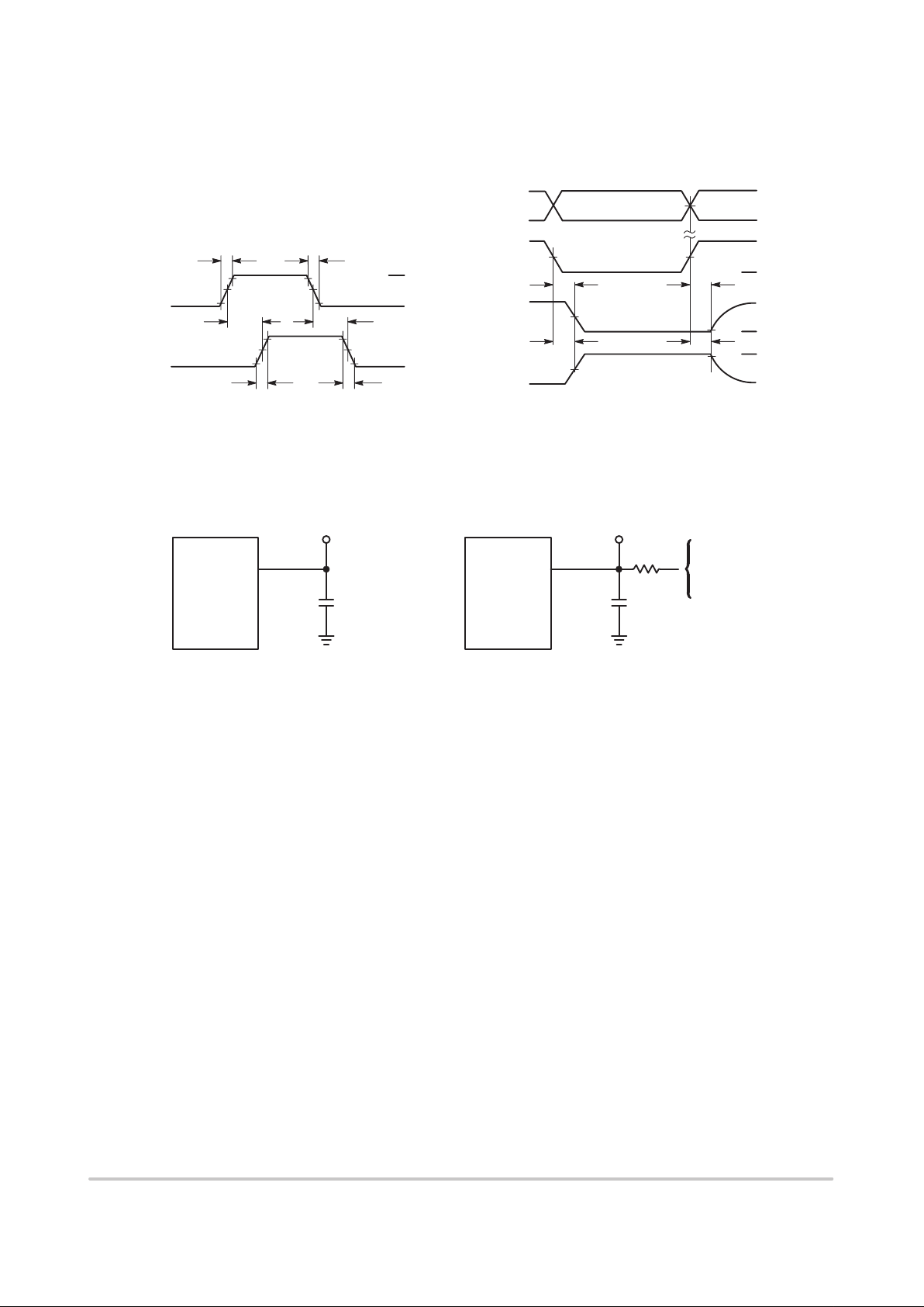
SWITCHING W AVEFORMS
V
CC
GND
t
f
t
r
INPUT
A OR B
OUTPUT
B OR A
10%
50%
90%
10%
50%
90%
t
TLH
t
PLH
t
PHL
t
THL
Figure 1.
OUTPUT
ENABLE
A OR B
A OR B
50%
50%
50%
90%
10%
t
PZL
t
PLZ
t
PZHtPHZ
V
CC
GND
HIGH
IMPEDANCE
V
OL
V
OH
HIGH
IMPEDANCE
V
CC
GND
50%
Figure 2.
DIRECTION
TEST CIRCUITS
*Includes all probe and jig capacitance
CL*
TEST POINT
DEVICE
UNDER
TEST
OUTPUT
Figure 3.
*Includes all probe and jig capacitance
CL*
TEST POINT
DEVICE
UNDER
TEST
OUTPUT
Figure 4.
CONNECT TO VCC WHEN
TESTING t
PLZ
AND t
PZL
.
CONNECT TO GND WHEN
TESTING t
PHZ
AND t
PZH
.
1 kΩ
MC74HC245A
http://onsemi.com
5
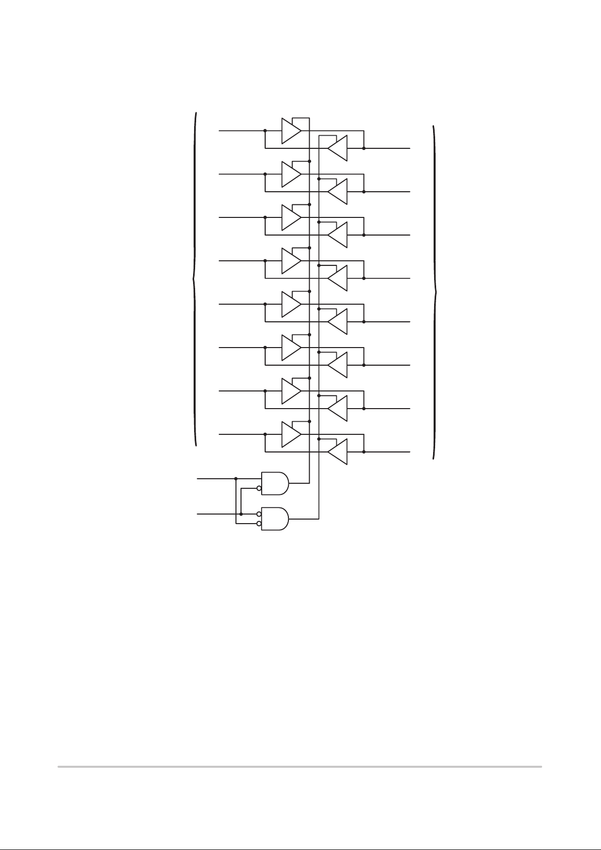
EXPANDED LOGIC DIAGRAM
A
DATA
PORT
B
DATA
PORT
OUTPUT ENABLE
DIRECTION
A1
A2
A3
A4
A5
A6
A7
A8
2
3
4
5
6
7
8
9
19
1
B1
B2
B3
B4
B5
B6
B7
B8
18
17
16
15
14
13
12
11
MC74HC245A
http://onsemi.com
6
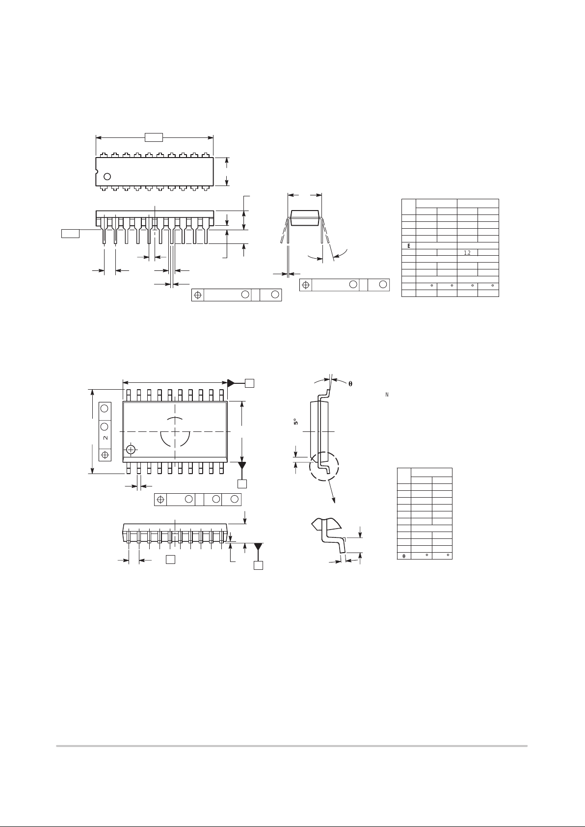
P ACKAGE DIMENSIONS
SO–20
DW SUFFIX
CASE 751D–05
ISSUE F
PDIP–20
N SUFFIX
PLASTIC DIP PACKAGE
CASE 738–03
ISSUE E
NOTES:
1. DIMENSIONING AND TOLERANCING PER ANSI
Y14.5M, 1982.
2. CONTROLLING DIMENSION: INCH.
3. DIMENSION L TO CENTER OF LEAD WHEN
FORMED PARALLEL.
4. DIMENSION B DOES NOT INCLUDE MOLD
FLASH.
M
L
J
20 PL
M
B
M
0.25 (0.010) T
DIM MIN MAX MIN MAX
MILLIMETERSINCHES
A 25.66 27.171.010 1.070
B 6.10 6.600.240 0.260
C 3.81 4.570.150 0.180
D 0.39 0.550.015 0.022
G 2.54 BSC0.100 BSC
J 0.21 0.380.008 0.015
K 2.80 3.550.110 0.140
L 7.62 BSC0.300 BSC
M 0 15 0 15
N 0.51 1.010.020 0.040
____
E
1.27 1.770.050 0.070
1
11
10
20
–A–
SEATING
PLANE
K
N
FG
D
20 PL
–T–
M
A
M
0.25 (0.010) T
E
B
C
F
1.27 BSC0.050 BSC
20
1
11
10
B20X
H10X
C
L
18X
A1
A
SEATING
PLANE
q
h X 45
_
E
D
M
0.25
M
B
M
0.25
SAS
B
T
e
T
B
A
DIM MIN MAX
MILLIMETERS
A 2.35 2.65
A1 0.10 0.25
B 0.35 0.49
C 0.23 0.32
D 12.65 12.95
E 7.40 7.60
e 1.27 BSC
H 10.05 10.55
h 0.25 0.75
L 0.50 0.90
q
0 7
NOTES:
1. DIMENSIONS ARE IN MILLIMETERS.
2. INTERPRET DIMENSIONS AND TOLERANCES
PER ASME Y14.5M, 1994.
3. DIMENSIONS D AND E DO NOT INCLUDE MOLD
PROTRUSION.
4. MAXIMUM MOLD PROTRUSION 0.15 PER SIDE.
5. DIMENSION B DOES NOT INCLUDE DAMBAR
PROTRUSION. ALLOWABLE PROTRUSION SHALL
BE 0.13 TOTAL IN EXCESS OF B DIMENSION AT
MAXIMUM MATERIAL CONDITION.
__

MC74HC245A
http://onsemi.com
7
Notes
MC74HC245A
http://onsemi.com
8
ON Semiconductor and are trademarks of Semiconductor Components Industries, LLC (SCILLC). SCILLC reserves the right to make changes
without further notice to any products herein. SCILLC makes no warranty , representation or guarantee regarding the suitability of its products for any particular
purpose, nor does SCILLC assume any liability arising out of the application or use of any product or circuit, and specifically disclaims any and all liability ,
including without limitation special, consequential or incidental damages. “Typical” parameters which may be provided in SCILLC data sheets and/or
specifications can and do vary in different applications and actual performance may vary over time. All operating parameters, including “Typicals” must be
validated for each customer application by customer’s technical experts. SCILLC does not convey any license under its patent rights nor the rights of others.
SCILLC products are not designed, intended, or authorized for use as components in systems intended for surgical implant into the body, or other applications
intended to support or sustain life, or for any other application in which the failure of the SCILLC product could create a situation where personal injury or
death may occur. Should Buyer purchase or use SCILLC products for any such unintended or unauthorized application, Buyer shall indemnify and hold
SCILLC and its officers, employees, subsidiaries, affiliates, and distributors harmless against all claims, costs, damages, and expenses, and reasonable
attorney fees arising out of, directly or indirectly , any claim of personal injury or death associated with such unintended or unauthorized use, even if such claim
alleges that SCILLC was negligent regarding the design or manufacture of the part. SCILLC is an Equal Opportunity/Affirmative Action Employer .
PUBLICATION ORDERING INFORMATION
CENTRAL/SOUTH AMERICA:
Spanish Phone: 303–308–7143 (Mon–Fri 8:00am to 5:00pm MST)
Email: ONlit–spanish@hibbertco.com
ASIA/PACIFIC : LDC for ON Semiconductor – Asia Support
Phone: 303–675–2121 (Tue–Fri 9:00am to 1:00pm, Hong Kong Time)
T oll Free from Hong Kong & Singapore:
001–800–4422–3781
Email: ONlit–asia@hibbertco.com
JAPAN: ON Semiconductor, Japan Customer Focus Center
4–32–1 Nishi–Gotanda, Shinagawa–ku, T okyo, Japan 141–8549
Phone: 81–3–5740–2745
Email: r14525@onsemi.com
ON Semiconductor Website: http://onsemi.com
For additional information, please contact your local
Sales Representative.
MC74HC245A/D
NORTH AMERICA Literature Fulfillment:
Literature Distribution Center for ON Semiconductor
P.O. Box 5163, Denver, Colorado 80217 USA
Phone: 303–675–2175 or 800–344–3860 T oll Free USA/Canada
Fax: 303–675–2176 or 800–344–3867 Toll Free USA/Canada
Email: ONlit@hibbertco.com
Fax Response Line: 303–675–2167 or 800–344–3810 T oll Free USA/Canada
N. American Technical Support: 800–282–9855 Toll Free USA/Canada
EUROPE: LDC for ON Semiconductor – European Support
German Phone: (+1) 303–308–7140 (M–F 1:00pm to 5:00pm Munich Time)
Email: ONlit–german@hibbertco.com
French Phone: (+1) 303–308–7141 (M–F 1:00pm to 5:00pm Toulouse T ime)
Email: ONlit–french@hibbertco.com
English Phone: (+1) 303–308–7142 (M–F 12:00pm to 5:00pm UK T ime)
Email: ONlit@hibbertco.com
EUROPEAN TOLL–FREE ACCESS*: 00–800–4422–3781
*Available from Germany, France, Italy , England, Ireland
 Loading...