

SEMICONDUCTOR TECHNICAL DATA
1
REV 6
Motorola, Inc. 1995
10/95
High–Performance Silicon–Gate CMOS
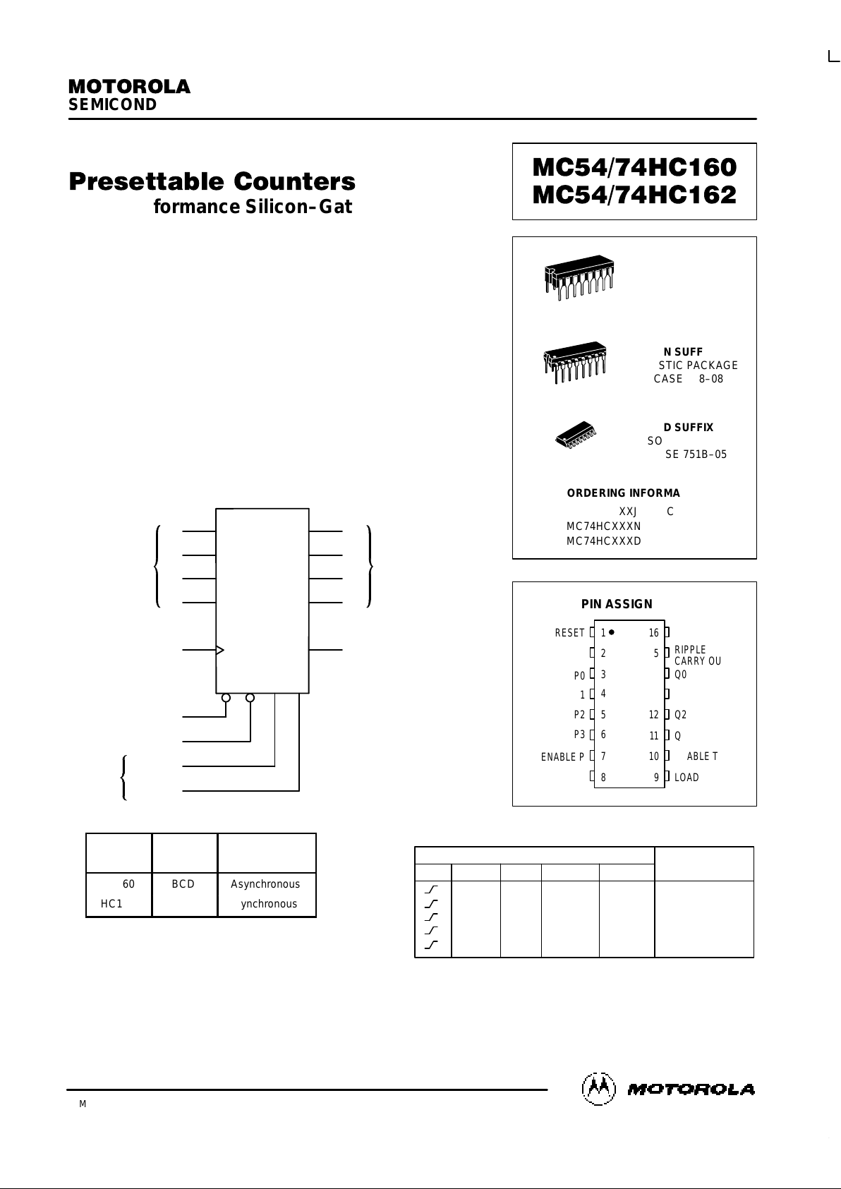
The MC54/74HC160 and HC162 are identical in pinout to the LS160 and
LS162, respectively. The device inputs are compatible with standard CMOS
outputs; with pullup resistors, they are compatible with LSTTL outputs.
The HC160 and HC162 are programmable BCD counters with asynchronous and synchronous Reset inputs, respectively.
• Output Drive Capability: 10 LSTTL Loads
• Outputs Directly Interface to CMOS, NMOS, and TTL
• Operating Voltage Range: 2 to 6 V
• Low Input Current: 1 µA
• High Noise Immunity Characteristic of CMOS Devices
• In Compliance with the Requirements Defined by JEDEC Standard
No. 7A
• Chip Complexity: 234 FETs or 58.5 Equivalent Gates
LOGIC DIAGRAM
PIN 16 = V
CC
PIN 8 = GND
11
12
13
14
Q0
Q1
Q2
Q3
15
RIPPLE
CARRY
OUT
BCD OR
BINARY
OUTPUTS
3
4
5
6
P0
P1
P2
P3
2
CLOCK
RESET
LOAD
ENABLE P
ENABLE T
COUNT
ENABLES
PRESENT
DATA
INPUTS
Device
Count
Mode
Reset Mode
HC160
BCD
Asynchronous
HC162
BCD
Synchronous
PIN ASSIGNMENT
13
14
15
16
9
10
11
12
5
4
3
2
1
8
7
6
RESET
P0
CLOCK
GND
Q1
Q0
RIPPLE
CARRY OUT
V
CC
P1
P2
P3
ENABLE P
Q2
Q3
ENABLE T
LOAD
D SUFFIX
SOIC PACKAGE
CASE 751B–05
N SUFFIX
PLASTIC PACKAGE
CASE 648–08
ORDERING INFORMATION
MC54HCXXXJ
MC74HCXXXN
MC74HCXXXD
Ceramic
Plastic
SOIC
1
16
1
16
J SUFFIX
CERAMIC PACKAGE
CASE 620–10
1
16
Inputs Output
Clock Reset* Load Enable P Enable T Q
L X X X Reset
H L X X Load Preset Data
H H H H Count
H H L X No Count
H H X L No Count
FUNCTION TABLE
*HC162 only. HC160 is an Asynchronous Reset Device
H = high level
L = low level
X = don’t care
MC54/74HC160 MC54/74HC162
MOTOROLA High–Speed CMOS Logic Data
DL129 — Rev 6
2
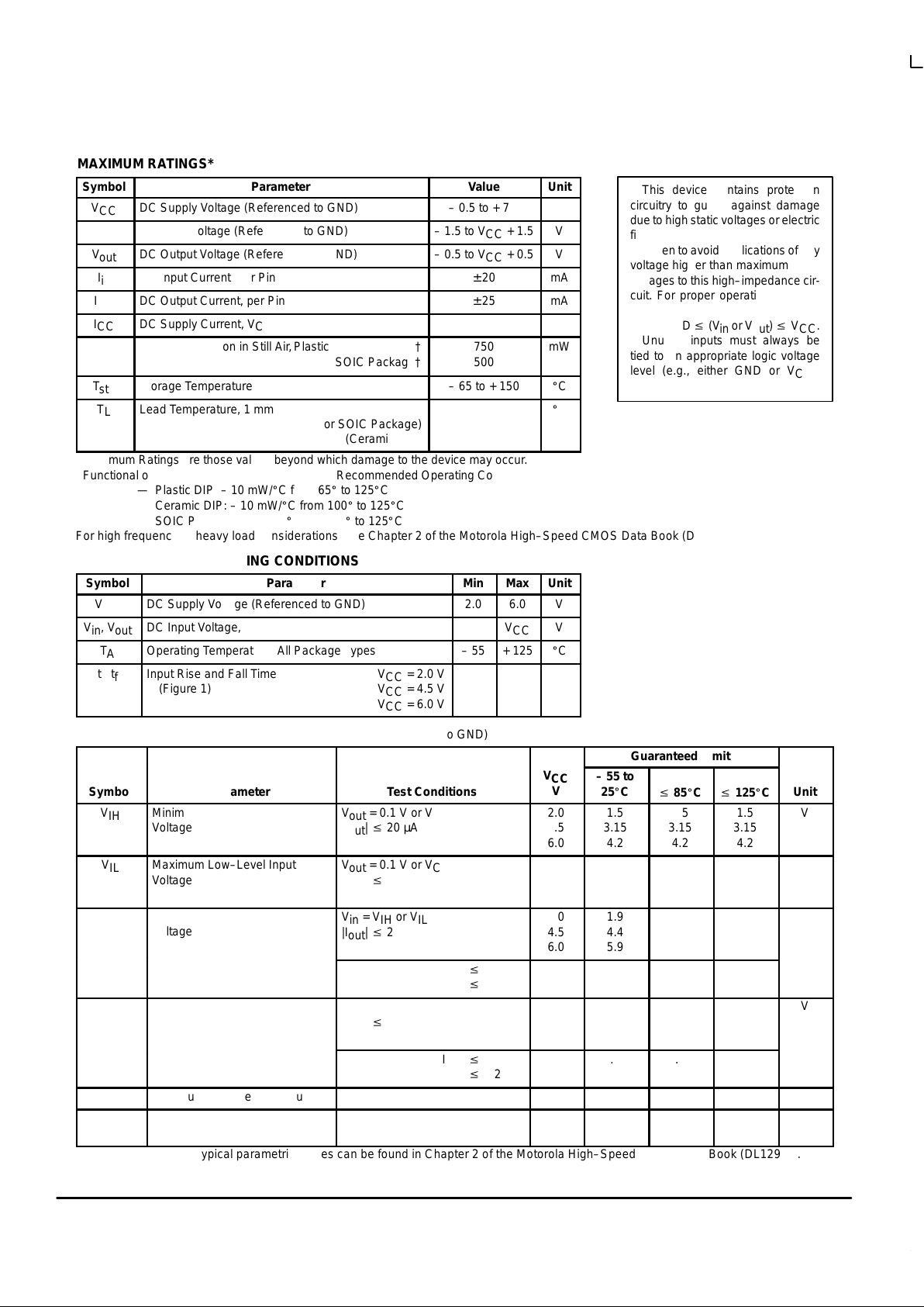
MAXIMUM RATINGS*
Symbol
Parameter
Value
Unit
V
CC
DC Supply Voltage (Referenced to GND)
– 0.5 to + 7.0
V
V
in
DC Input Voltage (Referenced to GND)
– 1.5 to VCC + 1.5
V
V
out
DC Output Voltage (Referenced to GND)
– 0.5 to VCC + 0.5
V
I
in
DC Input Current, per Pin
± 20
mA
I
out
DC Output Current, per Pin
± 25
mA
I
CC
DC Supply Current, VCC and GND Pins
± 50
mA
P
D
Power Dissipation in Still Air,Plastic or Ceramic DIP†
SOIC Package†
750
500
mW
T
stg
Storage Temperature
– 65 to + 150
_
C
T
L
Lead Temperature, 1 mm from Case for 10 Seconds
(Plastic DIP or SOIC Package)
(Ceramic DIP)
260
300
_
C
*Maximum Ratings are those values beyond which damage to the device may occur.
Functional operation should be restricted to the Recommended Operating Conditions.
†Derating — Plastic DIP: – 10 mW/_C from 65_ to 125_C
Ceramic DIP: – 10 mW/_C from 100_ to 125_C
SOIC Package: – 7 mW/_C from 65_ to 125_C
For high frequency or heavy load considerations, see Chapter 2 of the Motorola High–Speed CMOS Data Book (DL129/D).
RECOMMENDED OPERATING CONDITIONS
Symbol
Parameter
Min
Max
Unit
V
CC
DC Supply Voltage (Referenced to GND)
2.0
6.0
V
Vin, V
out
DC Input Voltage, Output Voltage (Referenced to GND)
0
V
CC
V
T
A
Operating Temperature, All Package Types
– 55
+ 125
_
C
tr, t
f
Input Rise and Fall Time VCC = 2.0 V
(Figure 1) VCC = 4.5 V
VCC = 6.0 V
0
0
0
1000
500
400
ns
DC ELECTRICAL CHARACTERISTICS (Voltages Referenced to GND)
Guaranteed Limit
Symbol
Parameter
Test Conditions
V
CC
V
– 55 to
25_C
v
85_Cv 125_C
Unit
V
IH
Minimum High–Level Input
Voltage
V
out
= 0.1 V or VCC – 0.1 V
|I
out
| v 20 µA
2.0
4.5
6.0
1.5
3.15
4.2
1.5
3.15
4.2
1.5
3.15
4.2
V
V
IL
Maximum Low–Level Input
Voltage
V
out
= 0.1 V or VCC – 0.1 V
|I
out
| v 20 µA
2.0
4.5
6.0
0.3
0.9
1.2
0.3
0.9
1.2
0.3
0.9
1.2
V
V
OH
Minimum High–Level Output
Voltage
Vin = VIH or V
IL
|I
out
| v 20 µA
2.0
4.5
6.0
1.9
4.4
5.9
1.9
4.4
5.9
1.9
4.4
5.9
V
Vin = VIH or VIL|I
out
| v 4.0 mA
|I
out
| v 5.2 mA
4.5
6.0
3.98
5.48
3.84
5.34
3.70
5.20
V
OL
Maximum Low–Level Output
Voltage
Vin = VIH or V
IL
|I
out
| v 20 µA
2.0
4.5
6.0
0.1
0.1
0.1
0.1
0.1
0.1
0.1
0.1
0.1
V
Vin = VIH or VIL|I
out
| v 4.0 mA
|I
out
| v 5.2 mA
4.5
6.0
0.26
0.26
0.33
0.33
0.40
0.40
I
in
Maximum Input Leakage Current
Vin = VCC or GND
6.0
± 0.1
± 1.0
± 1.0
µA
I
CC
Maximum Quiescent Supply
Current (per Package)
Vin = VCC or GND
I
out
= 0 µA
6.0
8
80
160
µA
NOTE: Information on typical parametric values can be found in Chapter 2 of the Motorola High–Speed CMOS Data Book (DL129/D).
This device contains protection
circuitry to guard against damage
due to high static voltages or electric
fields. However, precautions must
be taken to avoid applications of any
voltage higher than maximum rated
voltages to this high–impedance circuit. For proper operation, Vin and
V
out
should be constrained to the
range GND v (Vin or V
out
) v VCC.
Unused inputs must always be
tied to an appropriate logic voltage
level (e.g., either GND or VCC).
Unused outputs must be left open.
MC54/74HC160 MC54/74HC162
High–Speed CMOS Logic Data
DL129 — Rev 6
3 MOTOROLA
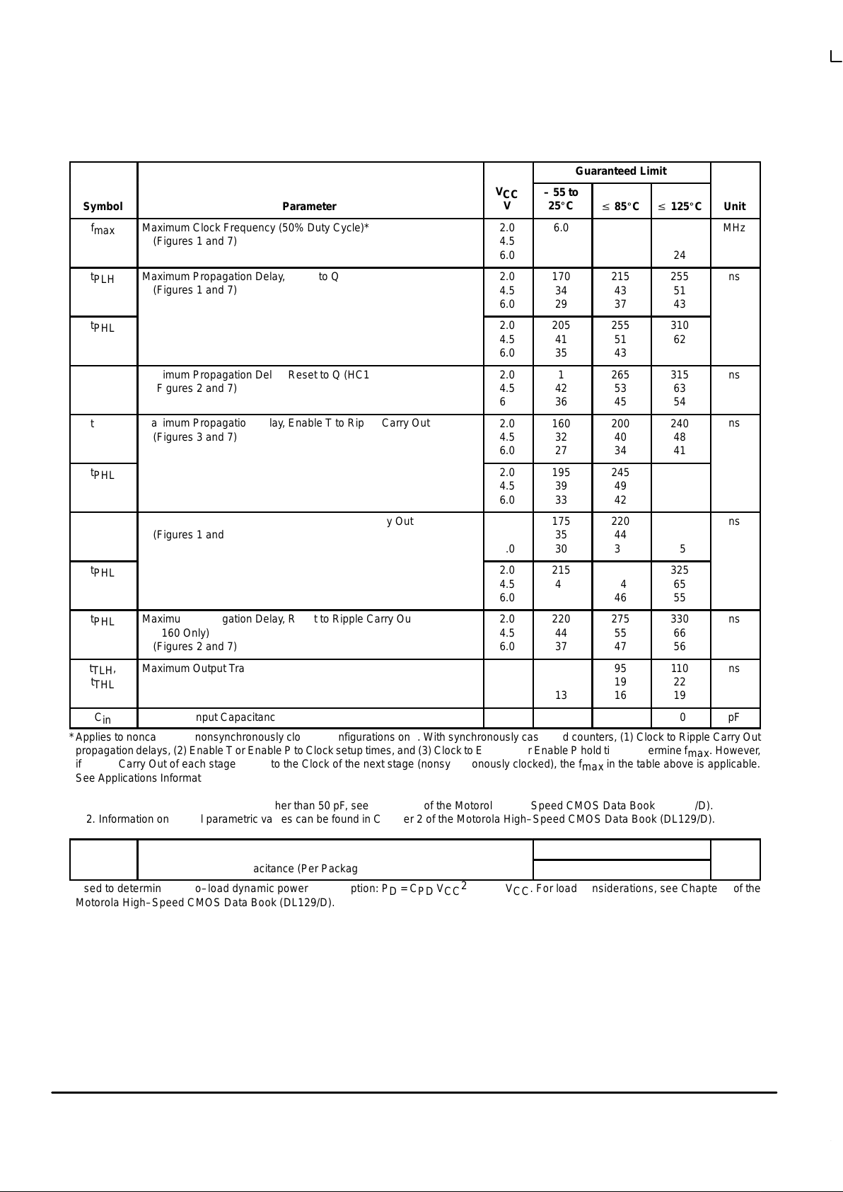
AC ELECTRICAL CHARACTERISTICS (C
L
= 50 pF, Input tr = tf = 6 ns)
Guaranteed Limit
Symbol
Parameter
V
CC
V
– 55 to
25_C
v
85_Cv 125_C
Unit
f
max
Maximum Clock Frequency (50% Duty Cycle)*
(Figures 1 and 7)
2.0
4.5
6.0
6.0
30
35
4.8
24
28
4.0
20
24
MHz
t
PLH
Maximum Propagation Delay, Clock to Q
(Figures 1 and 7)
2.0
4.5
6.0
170
34
29
215
43
37
255
51
43
ns
t
PHL
2.0
4.5
6.0
205
41
35
255
51
43
310
62
53
t
PHL
Maximum Propagation Delay, Reset to Q (HC160 Only)
(Figures 2 and 7)
2.0
4.5
6.0
210
42
36
265
53
45
315
63
54
ns
t
PLH
Maximum Propagation Delay, Enable T to Ripple Carry Out
(Figures 3 and 7)
2.0
4.5
6.0
160
32
27
200
40
34
240
48
41
ns
t
PHL
2.0
4.5
6.0
195
39
33
245
49
42
295
59
50
t
PLH
Maximum Propagation Delay, Clock to Ripple Carry Out
(Figures 1 and 7)
2.0
4.5
6.0
175
35
30
220
44
37
265
53
45
ns
t
PHL
2.0
4.5
6.0
215
43
37
270
54
46
325
65
55
t
PHL
Maximum Propagation Delay, Reset to Ripple Carry Out
(HC160 Only)
(Figures 2 and 7)
2.0
4.5
6.0
220
44
37
275
55
47
330
66
56
ns
t
TLH
,
t
THL
Maximum Output Transition Time, Any Output
(Figures 1 and 7)
2.0
4.5
6.0
75
15
13
95
19
16
110
22
19
ns
C
in
Maximum Input Capacitance
—
10
10
10
pF
*Applies to noncascaded/nonsynchronously clocked configurations only. With synchronously cascaded counters, (1) Clock to Ripple Carry Out
propagation delays, (2) Enable T or Enable P to Clock setup times, and (3) Clock to Enable T or Enable P hold times determine f
max
. However,
if Ripple Carry Out of each stage is tied to the Clock of the next stage (nonsynchronously clocked), the f
max
in the table above is applicable.
See Applications Information in this data sheet.
NOTES:
1. For propagation delays with loads other than 50 pF, see Chapter 2 of the Motorola High–Speed CMOS Data Book (DL129/D).
2. Information on typical parametric values can be found in Chapter 2 of the Motorola High–Speed CMOS Data Book (DL129/D).
Typical @ 25°C, VCC = 5.0 V
C
PD
Power Dissipation Capacitance (Per Package)*
60
pF
*Used to determine the no–load dynamic power consumption: PD = CPD V
CC
2
f + ICC VCC. For load considerations, see Chapter 2 of the
Motorola High–Speed CMOS Data Book (DL129/D).
MC54/74HC160 MC54/74HC162
MOTOROLA High–Speed CMOS Logic Data
DL129 — Rev 6
4
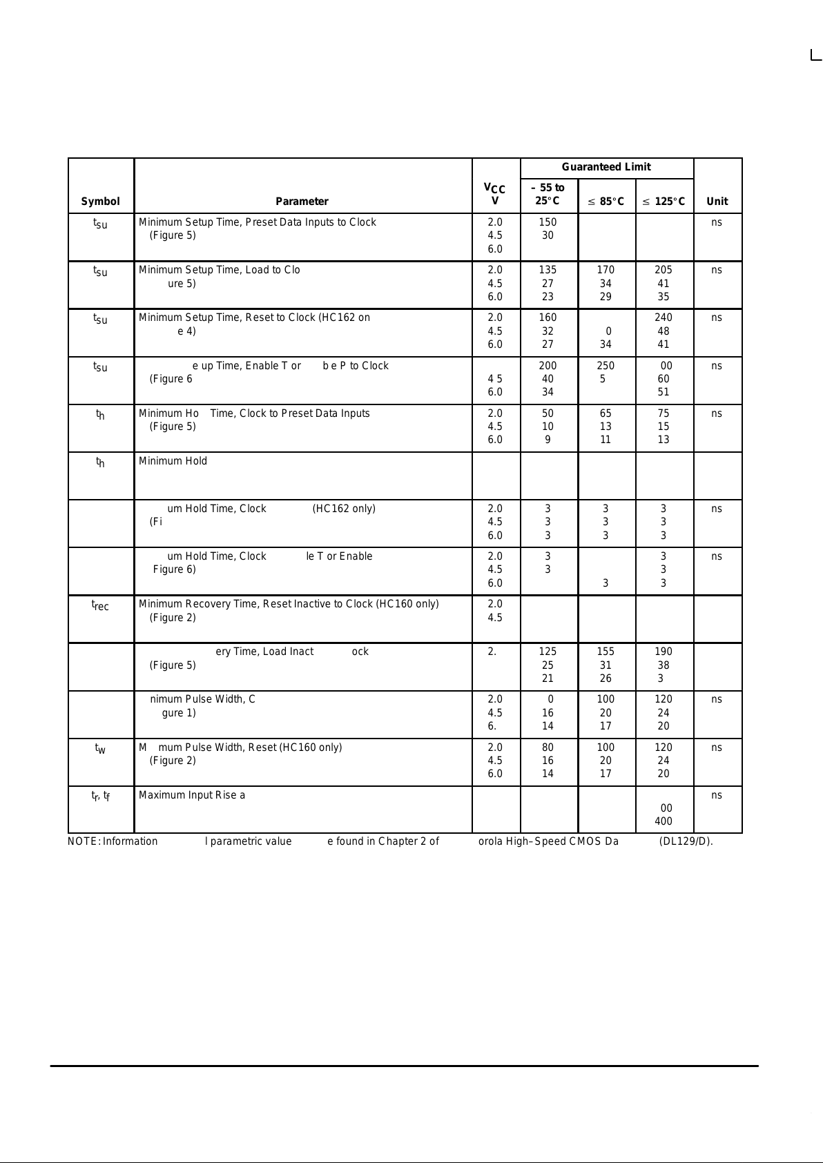
TIMING REQUIREMENTS (Input t
r
= tf = 6 ns)
Guaranteed Limit
Symbol
Parameter
V
CC
V
– 55 to
25_C
v
85_Cv 125_C
Unit
t
su
Minimum Setup Time, Preset Data Inputs to Clock
(Figure 5)
2.0
4.5
6.0
150
30
26
190
38
33
225
45
38
ns
t
su
Minimum Setup Time, Load to Clock
(Figure 5)
2.0
4.5
6.0
135
27
23
170
34
29
205
41
35
ns
t
su
Minimum Setup Time, Reset to Clock (HC162 only)
(Figure 4)
2.0
4.5
6.0
160
32
27
200
40
34
240
48
41
ns
t
su
Minimum Setup Time, Enable T or Enable P to Clock
(Figure 6)
2.0
4.5
6.0
200
40
34
250
50
43
300
60
51
ns
t
h
Minimum Hold Time, Clock to Preset Data Inputs
(Figure 5)
2.0
4.5
6.0
50
10
9
65
13
11
75
15
13
ns
t
h
Minimum Hold Time, Clock to Load
(Figure 5)
2.0
4.5
6.0
3
3
3
3
3
3
3
3
3
ns
t
h
Minimum Hold Time, Clock to Reset (HC162 only)
(Figure 4)
2.0
4.5
6.0
3
3
3
3
3
3
3
3
3
ns
t
h
Minimum Hold Time, Clock to Enable T or Enable P
(Figure 6)
2.0
4.5
6.0
3
3
3
3
3
3
3
3
3
ns
t
rec
Minimum Recovery Time, Reset Inactive to Clock (HC160 only)
(Figure 2)
2.0
4.5
6.0
125
25
21
155
31
26
190
38
32
ns
t
rec
Minimum Recovery Time, Load Inactive to Clock
(Figure 5)
2.0
4.5
6.0
125
25
21
155
31
26
190
38
32
ns
t
w
Minimum Pulse Width, Clock
(Figure 1)
2.0
4.5
6.0
80
16
14
100
20
17
120
24
20
ns
t
w
Minimum Pulse Width, Reset (HC160 only)
(Figure 2)
2.0
4.5
6.0
80
16
14
100
20
17
120
24
20
ns
tr, t
f
Maximum Input Rise and Fall Times
(Figure 1)
2.0
4.5
6.0
1000
500
400
1000
500
400
1000
500
400
ns
NOTE: Information on typical parametric values can be found in Chapter 2 of the Motorola High–Speed CMOS Data Book (DL129/D).

MC54/74HC160 MC54/74HC162
High–Speed CMOS Logic Data
DL129 — Rev 6
5 MOTOROLA
FUNCTION DESCRIPTION
The HC160/162 are p rogrammable 4–bit synchronous
counters that feature parallel Load, synchronous or asynchronous Reset, a Carry Output for cascading, and count–
enable controls.
The HC160 and HC162 are BCD counters with asynchronous Reset, and synchronous Reset, respectively.
INPUTS
Clock (Pin 2)
The internal flip–flops toggle and the output count advances with the rising edge of the Clock input. In addition,
control functions, such as resetting (HC162) and loading
occur with the rising edge of the Clock input.
Preset Data Inputs P0, P1, P2, P3 (Pins 3, 4, 5, 6)
These a re the data inputs f or programmable c ounting.
Data on these pins may be synchronously loaded into the internal flip–flops and appear at the counter outputs. P0 (pin 3)
is the least–significant bit and P3 (pin 6) is the most–significant bit.
OUTPUTS
Q0, Q1, Q2, Q3 (Pins 14, 13, 12, 11)
These are the counter outputs (BCD or binary). Q0 (pin 14)
is the least–significant bit and Q3 (pin 11) is the most–significant bit.
Ripple Carry Out (Pin 15)
When the counter is in its maximum state (1001 for the
BCD counters or 1111 for the binary counters), this output
goes high, providing an external look–ahead carry pulse that
may be used to enable successive cascaded counters. Ripple Carry Out remains high only during the maximum count
state. The logic equation for this output is:
Ripple Carry Out = Enable T Q0 Q1
Q2 Q3
for BCD counters HC160 and
HC162
CONTROL FUNCTIONS
Resetting
A low level on the Reset pin (pin 1) resets the internal flip–
flops and sets the outputs (Q0 through Q3) to a low level.
The HC160 resets asynchronously and the HC162 resets
with the rising edge of the Clock input (synchronous reset).
Loading
With the rising edge of the Clock, a low level on Load (pin
9) loads the data from the Preset Data Input pins (P0, P1, P2,
P3) into the internal flip–flops and onto the output pins, Q0
through Q3. The count function is disabled as long as Load is
low.
Although the HC160 and HC162 are BCD counters, they
may be programmed to any state. If they are loaded with a
state disallowed in BCD code, they will return to their normal
count s equence within two clock pulses (see the Output
State Diagram).
Count Enable/Disable
These devices have two count–enable control pins: Enable P (pin 7) and Enable T (pin 10). The devices count when
these two pins and the Load pin are high. The logic equation
is:
Count Enable = Enable P Enable T Load
The count is either enabled or disabled by the control inputs according to Table 1. In general, Enable P is a count–
enable control; E nable T i s both a c ount–enable a nd a
Ripple–Carry Output control.
Table 1. Count Enable/Disable
Control Inputs Result at Outputs
Load Enable P Enable T Q0 – Q3 Ripple Carry Out
H H H Count
High when Q0–Q3
L H H No Count
High when Q0–Q3
are maximum*
X L H No Count High when Q0–Q3
are maximum*
X X L No Count L
*Q0 through Q3 are maximum for the HC160 and HC162 when
Q3 Q2 Q1 Q0 = 1001.
HC160 and HC162 BCD Counters
0 1 2 3 4
5
6
7
89101112
13
14
15
OUTPUT STATE DIAGRAMS

MC54/74HC160 MC54/74HC162
MOTOROLA High–Speed CMOS Logic Data
DL129 — Rev 6
6
SWITCHING WAVEFORMS
Figure 1. Figure 2.
Figure 3. Figure 4. HC162 Only
Figure 5. Figure 6.
TEST CIRCUIT
Figure 7.
t
r
t
f
V
CC
GND
t
THL
t
TLH
ANY
OUTPUT
90%
50%
10%
90%
50%
10%
CLOCK
t
PLHtPHL
50%
t
PHL
V
CC
GND
V
CC
GND
ANY
OUTPUT
CLOCK
RESET
50%
50%
t
rec
t
r
t
f
V
CC
GND
t
PHL
t
PLH
90%
50%
10%
90%
50%
10%
t
THL
t
TLH
ENABLE T
RIPPLE
CARRY
OUT
CLOCK
RESET
50%
t
su
V
CC
GND
50%
INPUTS
P0, P1,
P2, P3
50%
V
CC
GND
V
CC
GND
GND
50%
50%
LOAD
CLOCK
V
CC
GND
V
CC
GND
ENABLE T
OR
ENABLE P
50%
50%
CLOCK
*Includes all probe and jig capacitance
CL*
TEST POINT
DEVICE
UNDER
TEST
OUTPUT
V
CC
t
w
1/fmax
t
w
t
h
VALID
t
su
t
h
t
su
t
h
t
rec
VALID
t
su
t
h

MC54/74HC160 MC54/74HC162
High–Speed CMOS Logic Data
DL129 — Rev 6
7 MOTOROLA
MC54HC160 MC74HC160•
BCD Counter with Asynchronous Reset
P0
P1
P2
P3
ENABLE P
ENABLE T
RESET
CLOCK
LOAD
R
C
T0RCCLOAD
LOAD
P0
Q0 Q0
Q1
Q2
Q3
RIPPLE
CARRY
OUT
V
CC
= PIN 16
GND = PIN 8
14
The flip–flops shown in the circuit diagrams are Toggle–Enable flip–flops. A Toggle–
Enable flip–flop is a combination of a D flip–flop and a T flip–flop. When loading data from
Preset inputs P0, P1, P2, and P3, the Load signal is used to disable the Toggle input (Tn) of
the flip–flop. The logic level at the Pn input is then clocked to the Q output of the flip–flop
on the next rising edge of the clock.
A logic zero on the Reset device input forces the internal clock (C) high and resets the Q
output of the flip–flop low.
C
LOAD
LOAD
Q0
Q1
Q1
Q2
Q2
Q3
Q3
T1RCCLOAD
LOADP1T2RCCLOAD
LOAD
P2
T3RCCLOAD
LOAD
P3
13
12
11
15
3
4
5
6
7
10
1
2
3

MC54/74HC160 MC54/74HC162
MOTOROLA High–Speed CMOS Logic Data
DL129 — Rev 6
8
HC160, HC162 TIMING DIAGRAM
Sequence illustrated in waveforms:
1. Reset outputs to zero.
2. Preset to BCD seven.
3. Count to eight, nine, zero, one, two, and three.
4. Inhibit.
RESET (HC160)
RESET (HC162)
LOAD
P0
P1
P2
P3
CLOCK (HC160)
CLOCK (HC162)
ENABLE P
ENABLE T
Q0
Q1
Q2
Q3
RIPPLE
CARRY
OUT
(ASYNCHRONOUS)
(SYNCHRONOUS)
7 8 9 0 1 2 3
RESET LOAD
COUNT
ENABLES
OUTPUTS
PRESET
DATA
INPUTS
INHIBITCOUNT

MC54/74HC160 MC54/74HC162
High–Speed CMOS Logic Data
DL129 — Rev 6
9 MOTOROLA
MC54HC160 MC74HC160•
BCD Counter with Synchronous Reset
P0
P1
P2
P3
ENABLE P
ENABLE T
RESET
CLOCK
LOAD
R
C
T0RCCLOAD
LOAD
P0
Q0 Q0
Q1
Q2
Q3
RIPPLE
CARRY
OUT
V
CC
= PIN 16
GND = PIN 8
14
The flip–flops shown in the circuit diagrams are Toggle–Enable flip–flops. A Toggle–
Enable flip–flop is a combination of a D flip–flop and a T flip–flop. When loading data from
Preset inputs P0, P1, P2, and P3, the Load signal is used to disable the Toggle input (Tn) of
the flip–flop. The logic level at the Pn input is then clocked to the Q output of the flip–flop
on the next rising edge of the clock.
A logic zero on the Reset device input forces the internal clock (C) high and resets the Q
output of the flip–flop low.
C
LOAD
LOAD
Q0
Q1
Q1
Q2
Q2
Q3
Q3
T1RCCLOAD
LOADP1T2RCCLOAD
LOAD
P2
T3RCCLOAD
LOAD
P3
13
12
11
15
3
4
5
6
7
10
1
2
3

MC54/74HC160 MC54/74HC162
MOTOROLA High–Speed CMOS Logic Data
DL129 — Rev 6
10
INPUTS
OUTPUTS
TO
MORE
SIGNIFICANT
STAGES
LOAD
H = COUNT
L = DISABLE
H = COUNT
L = DISABLE
RESET
CLOCK
LOAD P0 P1 P2 P3
ENABLE P
ENABLE T
CLOCK
R Q0 Q1 Q2 Q3
RIPPLE
CARRY
OUT
LOAD
RESET
CLOCK
ENABLE P
ENABLE T
TYPICAL APPLICATIONS
CASCADING
N–Bit Synchronous Counters
NOTE: When used in these cascaded configurations the clock f
max
guaranteed limits may not apply. Actual performance will depend on
number of stages. This limitation is due to set up times between Enable (Port) and Clock.
Nibble Ripple Counter
LOAD P0 P1 P2 P3
ENABLE P
ENABLE T
CLOCK
R Q0 Q1 Q2 Q3
RIPPLE
CARRY
OUT
LOAD P0 P1 P2 P3
ENABLE P
ENABLE T
CLOCK
R Q0 Q1 Q2 Q3
RIPPLE
CARRY
OUT
INPUTS
OUTPUTS
INPUTS
OUTPUTS
INPUTS INPUTS INPUTS
OUTPUTS OUTPUTS OUTPUTS
TO
MORE
SIGNIFICANT
STAGES
LOAD P0 P1 P2 P3
ENABLE P
ENABLE T
CLOCK
R Q0 Q1 Q2 Q3
RIPPLE
CARRY
OUT
LOAD P0 P1 P2 P3
ENABLE P
ENABLE T
CLOCK
R Q0 Q1 Q2 Q3
RIPPLE
CARRY
OUT
LOAD P0 P1 P2 P3
ENABLE P
ENABLE T
CLOCK
R Q0 Q1 Q2 Q3
RIPPLE
CARRY
OUT

MC54/74HC160 MC54/74HC162
High–Speed CMOS Logic Data
DL129 — Rev 6
11 MOTOROLA
Modulo–5 Counter
OUTPUT
OPTIONAL BUFFER
FOR NOISE REJECTION
OTHER
INPUTS
RESET
HC162
Q0
Q1
Q2
Q3
TYPICAL APPLICATION
The HC162 facilitates designing counters of any modulus with minimal external logic. The output is glitch–free due to the
synchronous Reset.

MC54/74HC160 MC54/74HC162
MOTOROLA High–Speed CMOS Logic Data
DL129 — Rev 6
12
OUTLINE DIMENSIONS
J SUFFIX
CERAMIC PACKAGE
CASE 620–10
ISSUE V
N SUFFIX
PLASTIC PACKAGE
CASE 648–08
ISSUE R
19.05
6.10
—
0.39
1.40
0.21
3.18
19.93
7.49
5.08
0.50
1.65
0.38
4.31
0
°
0.51
15
°
1.01
1.27 BSC
2.54 BSC
7.62 BSC
MIN MINMAX MAX
INCHES MILLIMETERS
DIM
0.750
0.240
—
0.015
0.055
0.008
0.125
0.785
0.295
0.200
0.020
0.065
0.015
0.170
0.050 BSC
0.100 BSC
0.300 BSC
A
B
C
D
E
F
G
J
K
L
M
N
0
°
0.020
15
°
0.040
NOTES:
1. DIMENSIONING AND TOLERANCING PER
ANSI Y14.5M, 1982.
2. CONTROLLING DIMENSION: INCH.
3. DIMENSION L TO CENTER OF LEAD WHEN
FORMED PARALLEL.
4. DIM F MAY NARROW TO 0.76 (0.030) WHERE
THE LEAD ENTERS THE CERAMIC BODY.
1 8
916
–A
–
–B
–
C
K
N
G
E
F
D 16 PL
–T
–
SEATING
PLANE
M
L
J 16 PL
0.25 (0.010) T A
M
S
0.25 (0.010) T B
M
S
MIN MINMAX MAX
INCHES MILLIMETERS
DIM
A
B
C
D
F
G
H
J
K
L
M
S
18.80
6.35
3.69
0.39
1.02
0.21
2.80
7.50
0
°
0.51
19.55
6.85
4.44
0.53
1.77
0.38
3.30
7.74
10
°
1.01
0.740
0.250
0.145
0.015
0.040
0.008
0.110
0.295
0
°
0.020
0.770
0.270
0.175
0.021
0.070
0.015
0.130
0.305
10
°
0.040
NOTES:
1. DIMENSIONING AND TOLERANCING PER ANSI
Y14.5M, 1982.
2. CONTROLLING DIMENSION: INCH.
3. DIMENSION L TO CENTER OF LEADS WHEN
FORMED PARALLEL.
4. DIMENSION B DOES NOT INCLUDE MOLD FLASH.
5. ROUNDED CORNERS OPTIONAL.
2.54 BSC
1.27 BSC
0.100 BSC
0.050 BSC
–A
–
B
1 8
916
F
H
G
D
16 PL
S
C
–T
–
SEATING
PLANE
K
J
M
L
T A0.25 (0.010)
M M
0.25 (0.010) T B A
M
S S
MIN MINMAX MAX
MILLIMETERS INCHES
DIM
A
B
C
D
F
G
J
K
M
P
R
9.80
3.80
1.35
0.35
0.40
0.19
0.10
0
°
5.80
0.25
10.00
4.00
1.75
0.49
1.25
0.25
0.25
7
°
6.20
0.50
0.386
0.150
0.054
0.014
0.016
0.008
0.004
0
°
0.229
0.010
0.393
0.157
0.068
0.019
0.049
0.009
0.009
7
°
0.244
0.019
1.27 BSC 0.050 BSC
NOTES:
1. DIMENSIONING AND TOLERANCING PER ANSI
Y14.5M, 1982.
2. CONTROLLING DIMENSION: MILLIMETER.
3. DIMENSIONS A AND B DO NOT INCLUDE
MOLD PROTRUSION.
4. MAXIMUM MOLD PROTRUSION 0.15 (0.006)
PER SIDE.
5. DIMENSION D DOES NOT INCLUDE DAMBAR
PROTRUSION. ALLOWABLE DAMBAR
PROTRUSION SHALL BE 0.127 (0.005) TOTAL
IN EXCESS OF THE D DIMENSION AT
MAXIMUM MATERIAL CONDITION.
1
8
916
–A
–
–B
–
D 16 PL
K
C
G
–T
–
SEATING
PLANE
R X 45°
M
J
F
P 8 PL
0.25 (0.010) B
M M
D SUFFIX
PLASTIC SOIC PACKAGE
CASE 751B–05
ISSUE J

MC54/74HC160 MC54/74HC162
High–Speed CMOS Logic Data
DL129 — Rev 6
13 MOTOROLA
How to reach us:
USA/EUROPE: Motorola Literature Distribution; JAPAN: Nippon Motorola Ltd.; Tatsumi–SPD–JLDC, Toshikatsu Otsuki,
P.O. Box 20912; Phoenix, Arizona 85036. 1–800–441–2447 6F Seibu–Butsuryu–Center, 3–14–2 Tatsumi Koto–Ku, Tokyo 135, Japan. 03–3521–8315
MFAX: RMFAX0@email.sps.mot.com –TOUCHTONE (602) 244–6609 HONG KONG: Motorola Semiconductors H.K. Ltd.; 8B Tai Ping Industrial Park,
INTERNET: http://Design–NET.com 51 Ting Kok Road, Tai Po, N.T., Hong Kong. 852–26629298
Motorola reserves the right to make changes without further notice to any products herein. Motorola makes no warranty , representation or guarantee regarding
the suitability of its products for any particular purpose, nor does Motorola assume any liability arising out of the application or use of any product or circuit,
and specifically disclaims any and all liability, including without limitation consequential or incidental damages. “T ypical” parameters can and do vary in different
applications. All operating parameters, including “T ypicals” must be validated for each customer application by customer’s technical experts. Motorola does
not convey any license under its patent rights nor the rights of others. Motorola products are not designed, intended, or authorized for use as components in
systems intended for surgical implant into the body, or other applications intended to support or sustain life, or for any other application in which the failure of
the Motorola product could create a situation where personal injury or death may occur. Should Buyer purchase or use Motorola products for any such
unintended or unauthorized application, Buyer shall indemnify and hold Motorola and its officers, employees, subsidiaries, affiliates, and distributors harmless
against all claims, costs, damages, and expenses, and reasonable attorney fees arising out of, directly or indirectly, any claim of personal injury or death
associated with such unintended or unauthorized use, even if such claim alleges that Motorola was negligent regarding the design or manufacture of the part.
Motorola and are registered trademarks of Motorola, Inc. Motorola, Inc. is an Equal Opportunity/Affirmative Action Employer.
MC54/74HC160/D
*MC54/74HC160/D*
◊
CODELINE
 Loading...