

4-36
FAST AND LS TTL DATA
4-BIT MAGNITUDE COMPARATOR
The MC54/74F85 is a 4-Bit Magnitude Comparator which compares two
4-Bit words (A0-A3, B0-B3), A3, B3 being the most significant inputs. Operation
is not restricted to binary codes; the device will work with any monotonic code.
Three Outputs are provided: “A greater than B” (0A > B), “A less than B” (0
A
< B), “A equal to B” (0A = B). Three Expander Inputs, IA > B, IA < B, IA = B, allow
cascading without external gates. For proper compare operation, the Expander Inputs to the least significant position must be connected as follows: IA <
B
= IA > B = L, IA = B = H. For serial (ripple) expansion the 0A > B, 0A < B Outputs
are connected respectively to the IA > B and IA = B inputs of the next most significant comparator, as shown in Figure 1. Refer to applications section of
data sheet for high speed method of comparing large words.
• High Impedance NPN Base Inputs for Reduced Loading (20 µA in
HIGH and LOW States)
• Magnitude Comparison of any Binary Words
• Serial or Parallel Expansion Without Extra Gating
• ESD
>
4000 Volts
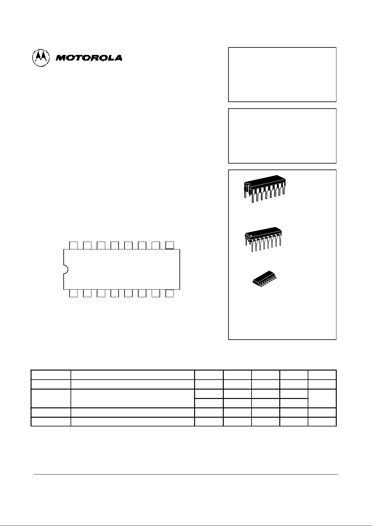
CONNECTION DIAGRAM
1516 14 13 12 11 10
21 3 4 5 6 7
V
CC
9
8
A3B2A2A1B1A0B
0
B3IA<BIA=BIA>BA>B A=B A<B GND
GUARANTEED OPERATING RANGES
Symbol Parameter Min Typ Max Unit
V
CC
Supply Voltage 54, 74 4.5 5.0 5.5 V
T
A
Operating Ambient Temperature Range
54 –55 25 125
°C
A
74 0 25 70
I
OH
Output Current High 54, 74 –1.0 mA
I
OL
Output Current Low 54, 74 20 mA
MC54/74F85
4-BIT MAGNITUDE COMPARATOR
FAST SCHOTTKY TTL
J SUFFIX
CERAMIC
CASE 620-09
N SUFFIX
PLASTIC
CASE 648-08
16
1
16
1
ORDERING INFORMATION
MC74FXXJ Ceramic
MC74FXXN Plastic
MC74FXXD SOIC
16
1
D SUFFIX
SOIC
CASE 751B-03
4-37
FAST AND LS TTL DATA
MC54/74F85
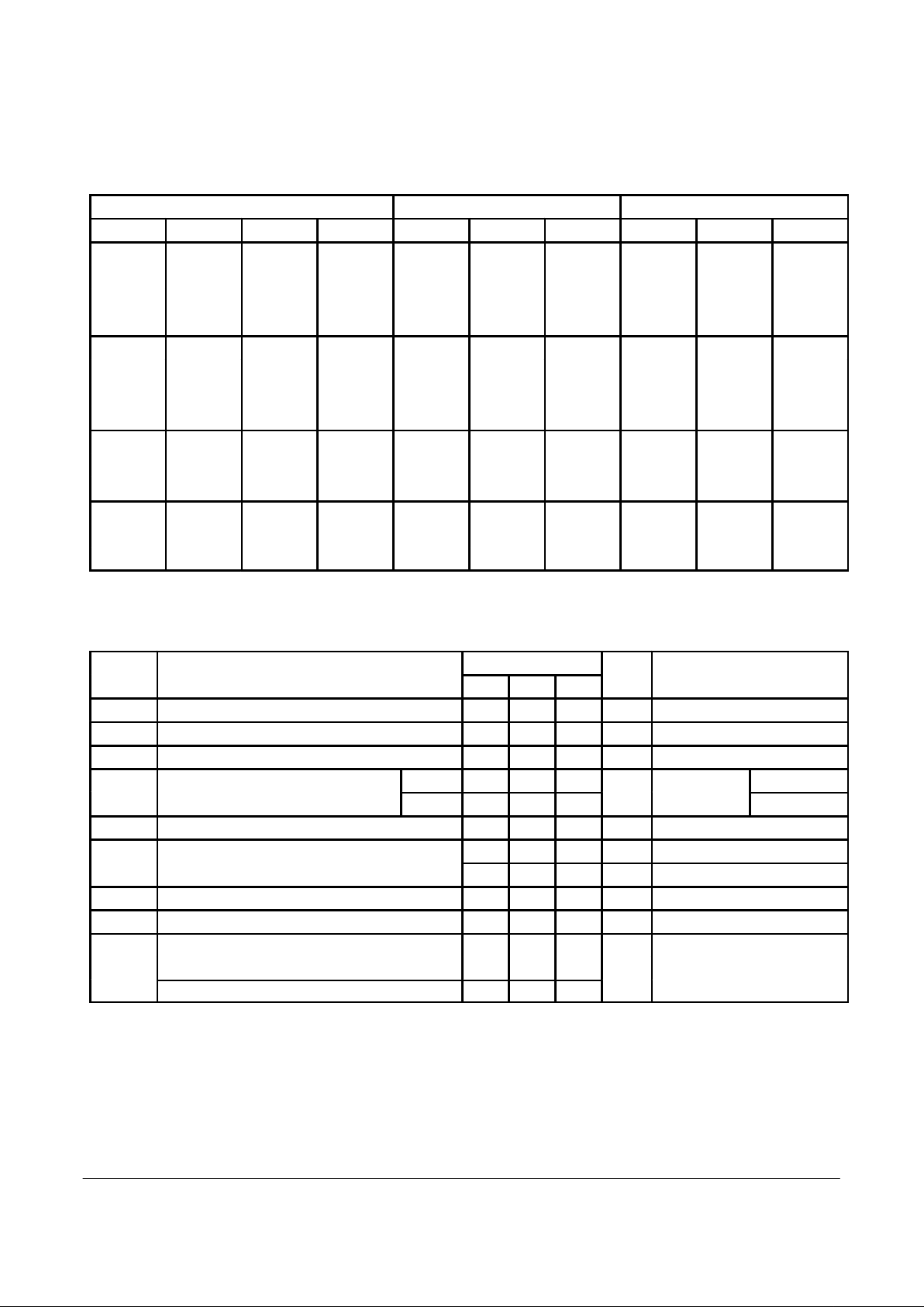
FUNCTION TABLE
Comparing Inputs Expansion Inputs Outputs
A3, B
3
A2, B
2
A1, B
1
A0, B
0
IA >
B
IA <
B
IA =
B
A > B A < B A = B
A3 > B
3
X X X X X X H L L
A3 < B
3
X X X X X X L H L
A3 = B
3
A2 > B
2
X X X X X H L L
A3 = B
3
A2 < B
2
X X X X X L H L
A3 = B
3
A2 = B
2
A1 > B
1
X X X X H L L
A3 = B
3
A2 = B
2
A1 < B
1
X X X X L H L
A3 = B
3
A2 = B
2
A1 = B
1
A0 > B
0
X X X H L L
A3 = B
3
A2 = B
2
A1 = B
1
A0 < B
0
X X X L H L
A3 = B
3
A2 = B
2
A1 = B
1
A0 = B
0
H L L H L L
A3 = B
3
A2 = B
2
A1 = B
1
A0 = B
0
L H L L H L
A3 = B
3
A2 = B
2
A1 = B
1
A0 = B
0
L L H L L H
A3 = B
3
A2 = B
2
A1 = B
1
A0 = B
0
X X H L L H
A3 = B
3
A2 = B
2
A1 = B
1
A0 = B
0
H H L L L L
A3 = B
3
A2 = B
2
A1 = B
1
A0 = B
0
L L L H H L
H = HIGH Voltage Level
L = LOW Voltage Level
X = Don’t Care
DC CHARACTERISTICS OVER OPERATING TEMPERATURE RANGE (unless otherwise specified)
Limits
Symbol Parameter Min Typ Max Unit Test Conditions
V
IH
Input HIGH Voltage 2.0 V Guaranteed Input HIGH Voltage
V
IL
Input LOW Voltage 0.8 V Guaranteed Input LOW Voltage
V
IK
Input Clamp Diode Voltage –1.2 V VCC = MIN, IIN = –18 mA
V
OH
Output HIGH Voltage 54, 74 2.5 V IOH = –1.0 mA VCC = 4.50 V
74 2.7 VCC = 4.75 V
V
OL
Output LOW Voltage 0.5 V IOL = 20 mA, VCC = MIN
I
IH
Input HIGH Current 20 µA VCC = MAX, VIN = 2.7 V
0.1 mA VCC = 0 V, VIN = 7.0 V
I
IL
Input LOW Current –20 µA VCC = MAX, VIN = 0.5 V
I
OS
Output Short Circuit Current (Note 2) –60 –150 mA VCC = MAX, V
OUT
= 0 V
Total Supply Current
I
CC
HIGH VIN = HIGH 50
mA VCC = MAX
LOW An = Bn = I
A-B
= GND: I
A>B
= I
A<B
= 4.5 V 54
CC
= MAX
NOTES:
1. For conditions shown as MIN or MAX, use the appropriate value specified under recommended operating conditions for the applicable device type.
2. Not more than one output should be shorted at a time, nor for more than 1 second.
4-38
FAST AND LS TTL DATA
MC54/74F85
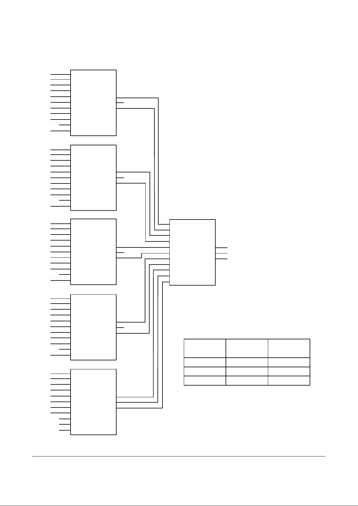
The parallel expansion scheme shown in Figure 1 demonstrates the most efficient general use of these comparators.
In the parallel expansion scheme, the expansion inputs can
be used as a fifth input bit position except on the least significant device which must be connected as in the Serial
Scheme. The expansion inputs are used by labelling I
A>B
as an “A” input, I
A<B
as a “B” input and setting I
A=B
low. The
‘F85 can be used as a 5-bit comparator only when the outputs are used to drive the (A0-A3) and (B0-B3) inputs of
another ‘F85 device. The parallel technique can be expanded to any number of bits as shown in Table 1.
Table 1
Word
Length
Number of
Packages
Typical Speeds
74F
1–4 Bits 1
22 ns
NC
NC
NC
NC
(MSB) B
23
A
23
B
22
A
22
B
21
A
21
B
20
A
20
A
19
L
B
19
B
3
A
3
B
2
A
2
B
1
A
1
B
0
A
0
IA <
B
IA =
B
IA >
B
A < B
A > B
A = B
B
18
B
17
B
16
B
15
B
14
B
13
B
12
B
11
B
10
B
9
B
8
B
7
B
6
B
5
B
4
B
3
B
2
B
1
B
0
A
18
A
17
A
16
A
15
A
14
A
13
A
12
A
11
A
10
A
9
A
8
A
7
A
6
A
5
A
4
A
3
A
2
A
1
A
0
L
L
L
L
H
L
B
3
A
3
B
2
A
2
B
1
A
1
B
0
A
0
IA <
B
IA =
B
IA >
B
A < B
A > B
A = B
B
3
A
3
B
2
A
2
B
1
A
1
B
0
A
0
IA <
B
IA =
B
IA >
B
A < B
A > B
A = B
B
3
A
3
B
2
A
2
B
1
A
1
B
0
A
0
IA <
B
IA =
B
IA >
B
B
3
A
3
B
2
A < B
A > B
A = B
A
2
B
1
A
1
B
0
A
0
IA <
B
IA =
B
IA >
B
A < B
A > B
A = B
B
3
A
3
B
2
A
2
B
1
A
1
B
0
A
0
A < B
A = B
A > B
A < B
A > B
A = B
OUTPUTS
(LSB)
Figure 1. Comparison of Two 24-Bit Words
5–25 Bits
25–120 Bits
2–6
34 ns
12 ns
8–31

4-39
FAST AND LS TTL DATA
MC54/74F85
AC ELECTRICAL CHARACTERISTICS
54/74F 54F 74F
TA = +25°C
VCC = +5.0 V
CL = 50 pF
TA = –55°C to +125°C
VCC = 5.0 V ± 10%
CL = 50 pF
TA = 0°C to + 70°C
VCC = 5.0 V ± 10%
CL = 50 pF
Symbol Parameter Min Max Min Max Min Max Unit
t
PLH
A or B Input to 6.0 11 5.5 14 5.5 13
t
PHL
A < B, A > B Output 6.0 14 5.5 16.5 5.5 15.5
ns
t
PLH
A or B Input to 5.5 11.5 5.0 15 5.0 14
t
PHL
A = B Output 7.0 14 6.5 15.5 6.5 14.5
ns
t
PLH
I
A<B
and I
A=B
Input 3.0 7.5 2.5 10 2.5 9.0
t
PHL
to A>B Output 3.0 9.0 2.5 11 2.5 10
ns
t
PLH
I
A=B
Input to 2.5 7.0 2.0 10 2.0 9.0
t
PHL
A = B Output 3.5 10 2.5 13 2.5 12
ns
t
PLH
I
A>B
and I
A=B
Input 3.0 8.0 3.0 10.5 3.0 9.5
t
PHL
to A<B Output 3.0 9.0 2.0 10.5 2.0 9.5
ns
The expansion inputs I
A>B
, I
A=B
, and I
A<B
are the least significant bit positions. When used for series expansion, the
A>B, A=B, and A<B outputs of the least significant word are
connected to the corresponding I
A>B
, I
A=B
, and I
A<B
inputs of
the next higher stage. Stages can be added in this manner
to any length, but a propagation delay penalty of about 15 ns
is added with each additional stage. For proper operation the
expansion inputs of the least significant word should be tied
as follows: I
A>B
= LOW, I
A=B
= HIGH, and I
A<B
= LOW.
IA <
B
IA =
B
IA >
B
NOTE:
This diagram is provided only for the understanding of logic operations and should not be used
to estimate propagation delays.
Figure 2. Logic Diagram
(15)
(1)
A
3
B
3
A
2
B
2
(13)
(14)
A
1
B
1
(12)
(11)
(2)
(3)
(4)
(5)
(6)
(7)
A > B
A = B
A < B
A
0
B
0
(10)
(9)
 Loading...