


For:char
Printed on:Mon, Feb 6, 1995 09:48:26
From book:DL121CH4 (5) VIEW
Document:MC74F323 (5) VIEW
Last saved on:Fri, Feb 3, 1995 16:04:13
4-150
FAST AND LS TTL DATA
8-INPUT SHIFT/STORAGE
REGISTER WITH SYNCHRONOUS
RESET AND COMMON I/O PINS
The MC74F323 is an 8-Bit Universal Shift/Storage Register with 3-state
outputs. Its function is similar to the F299 with the exception of Synchronous
Reset.
The parallel load inputs and flip-flop outputs are multiplexed to reduce the
total number of package pins. Separate outputs are provided for flip-flops Q
0
and Q7 to allow easy cascading. A separate active LOW Master Reset is used
to reset the register.
Four modes of operation are possible: hold (store), shift left, shift right and
parallel load. All modes are activated on the LOW-to-HIGH transition of the
clock.
• Common I/O For Reduced Pin Count
• Four Operation Modes: Shift Left, Shift Right, Parallel Load and Store
• Separate Continuous Inputs and Outputs from Q
0
and Q7 Allow Easy
Cascading
• Fully Synchronous Reset
• 3-State Outputs for Bus Oriented Applications
• Input Clamp Diodes Limit High-Speed Termination Effects
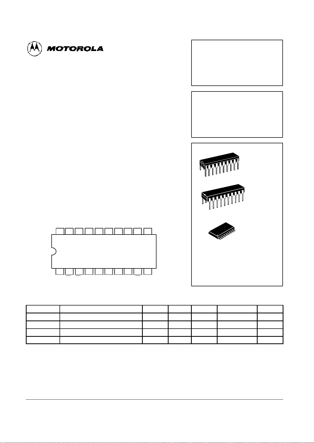
CONNECTION DIAGRAM
18 17 16 15 14 13
1 2 3 4 5 6
7
20 19
8
V
CC
S
0
S1DS7Q7I/O
7
I/O
3
I/O
5
I/O
1
OE
1OE2
I/O6I/O4I/O2I/O0Q
0
9 10
SR
GND
12 11
CP DS
0
GUARANTEED OPERATING RANGES
Symbol Parameter Min Typ Max Unit
V
CC
Supply Voltage 74 4.5 5.0 5.5 V
T
A
Operating Ambient Temperature Range 74 0 25 70 °C
I
OH
Output Current — High 74 –1.0/–3.0 mA
I
OL
Output Current — Low 74 20/24 mA
MC74F323
8-INPUT SHIFT/STORAGE
REGISTER WITH SYNCHRONOUS
RESET AND COMMON I/O PINS
FAST SCHOTTKY TTL
ORDERING INFORMATION
MC74FXXXJ Ceramic
MC74FXXXN Plastic
MC74FXXXDW SOIC
20
1
J SUFFIX
CERAMIC
CASE 732-03
20
1
N SUFFIX
PLASTIC
CASE 738-03
20
1
DW SUFFIX
SOIC
CASE 751D-03
 Loading...